

Page 1

INTEGRATED CIRCUITS
DATA SH EET
TEA5762
Self tuned radio
Preliminary specification
File under Integrated Circuits, IC01
1995 Jun 23
Page 2

Philips Semiconductors Preliminary specification
Self tuned radio TEA5762
FEATURES
• The tuning system has an optimized IC partitioning both
from application (omitting interferences) and flexibility
(removable front panel option) point of view: the tuning
synthesizer is on-chip with the radio
• The tuning quality is superior and requires no IF counter
for stop-detection; it is insensitive to ceramic filter
tolerances
• In combination with the microcontroller, fast, low-power
operation of preset mode, manual search, automatic
search and automatic store are possible
• The local (internal) controller function facilitates reduced
and simplified microcontroller software
• The high integration level means fewer external
components with regard to the communication between
the radio and the microcontroller and a simple and small
printed-circuit board (PCB)
• The inherent FUZZY LOGIC behaviour of STR (Self
Tuned Radio), which mimics hand tuning, yields a
potentially fast yet reliable tuning operation
• The level of the incoming signal at which the radio must
lock is software programmable
• Two programmable ports
• FM-on/off port to control the external FM front end
• High selectivity with distributed IF gain
• Soft mute
• Signal dependent stereo-blend
• High impedance MOSFET input on AM
• Wide supply voltage range of 2.5 to 12 V
• Low current consumption 18 mA at AM and FM
(including tuning synthesizer for AM)
• Low noise figure
• Low output distortion
• Due to the new tuning concept, the tuning is
independent of the channel spacing.
GENERAL DESCRIPTION
The TEA5762 is a 44-pin integrated AM-radio and FM-IF
and demodulator part including a novel tuning concept.
The radio part is based on the TEA5712.
It is designed for the use with an external FM-front end.
The new tuning concept combines the advantages of hand
tuning with electronic facilities and features. User
intelligence is incorporated into the tuning algorithm and
an improvement of the analog signal processing is used for
the AFC function.
ORDERING INFORMATION
TYPE
NUMBER
TEA5762H QFP44 plastic quad flat package; 44 leads (lead length 1.3 mm); body 10 × 10× 1.75 mm SOT307-2
1995 Jun 23 2
NAME DESCRIPTION VERSION
PACKAGE
Page 3

Philips Semiconductors Preliminary specification
Self tuned radio TEA5762
QUICK REFERENCE DATA
SYMBOL PARAMETER CONDITIONS MIN. TYP. MAX. UNIT
V
CC1
V
CC2
V
tune
I
CC1
I
DDD
I
CC2
T
amb
AM performance; note 1
V
10
V
i1
THD total harmonic distortion V
FM performance; note 2
V
10
V
i4
THD total harmonic distortion IF filter
supply voltage 1 2.5 − 12 V
supply voltage 2 for tuning −−12 V
tuning voltage 0.7 − V
CC2
− 0.75 V
supply current 1 AM mode 12 15 18 mA
FM mode 13 16 19 mA
digital supply current AM mode − 3.3 − mA
FM mode − 2.7 − mA
supply current 2 for tuning in preset
−−640 µA
mode (band-end to band-end)
operating ambient temperature −15 − +60 °C
AF output voltage Vi1=5mV 364570 mV
RF sensitivity input voltage S/N = 26 dB 40 55 70 µV
=1mV − 0.8 2.0 %
i1
AF output voltage Vi4=5mV 404857 mV
IF sensitivity input voltage V10= −3 dB;
− 20 30 µV
V10= 0 dB at Vi4=10mV
− 0.3 0.8 %
SFE10.7MS3A20K-A
MPX performance; note 3
α
cs
channel separation Vi4=30mV 26 30 − dB
Notes
1. Conditions AM: V
CC1
=3V; V
CC2
=12V; V
=3V; fi= 1 MHz; m = 0.3; fm= 1 kHz; measured in Fig.8 with S1 in
DDD
position A and S2 in position B; unless otherwise specified.
2. Conditions FM: V
CC1
=3V; V
CC2
= 12 V; V
=3V; fi= 10.7 MHz; ∆fm= 22.5 kHz; fm= 1 kHz; measured in Fig.8
DDD
with S2 in position A and S3 in position A; unless otherwise specified.
3. Conditions MPX: V
CC1
=3V; V
CC2
=12V; V
DDD
=3V; V
i3(L+R)
= 155 mV; V
Fig.8 with S2 in position B and S3 in position B; unless otherwise specified.
= 15.5 mV; fi= 1 kHz; measured in
pilot
1995 Jun 23 3
Page 4
Philips Semiconductors Preliminary specification
Self tuned radio TEA5762
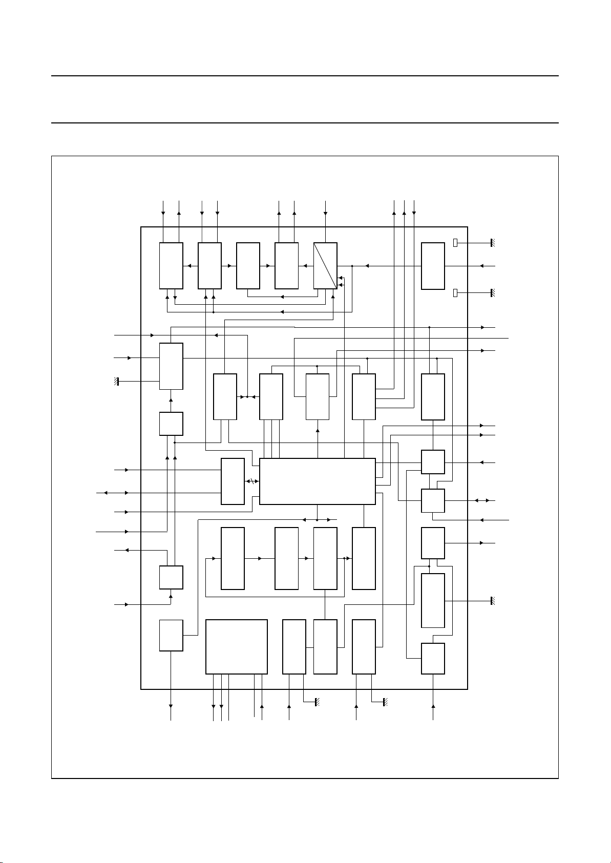
BLOCK DIAGRAM
(n)
(p)
PILFIL
MO/ST
LFI
VCO
AFLO
AFRO
MUTE
AFC
AFC
AFC
MBE815
BUS-
DATAFM-IF2I
WRITE-
IFGND FSIFMDEM
CLOCK
ENABLE
16
PILOT
12
24
DETECTOR
19 kHz
PLL
9
38 kHz
stereo
DECODER
14
MATRIX
15
mono
stereo
13
MUTE
SDS
TEA5762
21
1817272829333537
FM
DETECTOR
hard mute level
AFC
FM
IF2
AM/FM
INDICATOR
STATUS
REGISTER
IN-LOCK
DETECTOR
up
down
level
PUMP
CHARGE
CIRCUIT
SEQUENTIAL
FM
AM
32
20
19
V/I
CONVERTER
10 11 342
CC2
V
TUNE RFGND2 RFGND1MPXIAFO
AM
DETECTOR
P0
P1AGCAM-IF2I/OAM-MIXERAMOSC
handbook, full pagewidth
Fig.1 Block diagram.
AM
AM
AGC
IF
AM-IF1I
MIXER
FM-IFI1 FM-IFO1
1995 Jun 23 4
FM
IF1
TUNER
SWITCH
39
FM-ON/OFF
SHIFT REGISTER
38
34
7
CC1
V
STAB(A)VSTAB(B)
V
STABILIZER
1
23
DDD
V
RIPPLE
MEMORY
LAST-STATION
5
COUNTI
PROGRAMMABLE
PRESCALER
4
WINDOW
COUNTER
MULTIPLEXER
CGND
CRYSTAL
25
XTAL
DETECTOR
OSCILLATOR
26
DGND
AM
OSCILLATOR
AM
END
FRONT
2
AM-RFI
6404136443130 822
Page 5

Philips Semiconductors Preliminary specification
Self tuned radio TEA5762
PINNING
SYMBOL PIN DESCRIPTION
RIPPLE 1 ripple capacitor input
AM-RFI 2 AM-RF input
RFGND1 3 RF ground 1 and substrate
CGND 4 counter ground
COUNTI 5 counter input
AMOSC 6 parallel tuned AM oscillator circuit to ground
V
CC1
TUNE 8 tuning output current
VCO 9 voltage controlled oscillator input
AFO 10 AM/FM AF output (output impedance typical 5 kΩ)
MPXI 11 stereo decoder input (input impedance typical 150 kΩ)
LFI 12 loop-filter input
MUTE 13 mute input
AFLO 14 left channel output (output impedance typical 4.3 kΩ)
AFRO 15 right channel output (output impedance typical 4.3 kΩ)
PILFIL 16 pilot detector filter input
IFGND 17 ground of IF, detector and MPX stage
FMDEM 18 ceramic discriminator input
AFC
(n)
AFC
(p)
FSI 21 field-strength indicator
V
CC2
V
DDD
MO/ST 24 mono/stereo and tuning indication output
XTAL 25 crystal input
DGND 26 digital ground
BUS-CLOCK 27 bus-clock input
DATA 28 bus data input/output
WRITE-ENABLE 29 bus write enable input
P0 30 programmable output port (P0)
P1 31 programmable output port (P1)
AFC 32 450 kHz LC input circuit for AM AFC
FM-IF2I 33 FM-IF input 2 (input impedance typical 330 Ω)
V
STAB(B)
FM-IFO1 35 FM-IF output 1 (input impedance typical 330 Ω)
AM-IF2I/O 36 input/output to IFT; output current source
FM-IFI1 37 FM-IF input 1 (input impedance typical 330 Ω)
V
STAB(A)
FM-ON/OFF 39 FM ON/OFF port
AM-MIXER 40 open-collector output to IFT
7 supply voltage 1
19 AFC negative output
20 AFC positive output
22 supply voltage 2 (for tuning)
23 digital supply voltage
34 internal stabilized supply voltage (B)
38 internal stabilized supply voltage (A)
1995 Jun 23 5
Page 6

Philips Semiconductors Preliminary specification
Self tuned radio TEA5762
SYMBOL PIN DESCRIPTION
AM-IF1I 41 IFT or ceramic filter input (input impedance typical 3 kΩ)
RFGND2 42 FM-RF ground 2
n.c. 43 not connected
AGC 44 AGC capacitor input
handbook, full pagewidth
RIPPLE
AM-RFI
RFGND1
CGND
COUNTI
AMOSC
V
CC1
TUNE
VCO
AFO
MPXI
AGC
n.c.
RFGND2
AM-IF1I
AM-MIXER
44
43
42
41
40
1
2
3
4
5
15
AFRO
TEA5762
16
PILFIL
6
7
8
9
10
11
12
13
14
LFI
MUTE
AFLO
STAB(A)
FM-ON/OFF
V
39
38
17
18
IFGND
FMDEM
FM-IFI1
37
19
(n)
AFC
AM-IF2I/O
36
20
(p)
AFC
STAB(B)
FM-IFO1
V
35
34
21
22
FSI
CC2
V
33
FM-IF2I
32
AFC
31
P1
30
P0
29
WRITE-ENABLE
28
DATA
BUS-CLOCK
27
26
DGND
25
XTAL
24
MO/ST
23
V
DDD
MBE820
1995 Jun 23 6
Fig.2 Pin configuration.
Page 7

Philips Semiconductors Preliminary specification
Self tuned radio TEA5762
FUNCTIONAL DESCRIPTION
The TEA5762 is an integrated radio circuit with
AM-receiver and FM-IF part with demodulator and stereo
decoder. The circuit includes digital tuning and control
functions.
The radio
The AM circuit incorporates a double balanced mixer,
a one-pin low voltage oscillator (up to 30 MHz) and is
designed for distributed selectivity.
The AM input is designed to be connected to the top of
a tuned circuit. AGC controls the IF amplification and for
large signals it lowers the input impedance of the
AM front end.
The first AM selectivity can be an IF-Tank (IFT) or an IFT
combined with a ceramic filter; the second one is an IFT.
For FM operation an external FM front end is necessary.
This is switched on and off by the FM-ON/OFF signal
which is generated in the bus system.
The AFC circuit in the TEA5762 provides a tuning voltage
to drive the VCO of the external FM front end.
The frequency of the external VCO is counted in the Self
Tuned Radio (STR) tuning system.
The FM-IF circuit is designed for distributed IF ceramic
filters. The FM quadratic detector uses a ceramic
resonator.
The PLL stereo decoder incorporates a signal dependent
stereo-blend circuit and a soft-mute circuit.
Tuning
The tuning-concept of STR is based on FUZZY LOGIC:
it mimics hand tuning (hand tuning is a combination of
coarse and fine tuning to the qualitatively best frequency
position). As a consequence the tuning system is very fast.
The tuning algorithm, which is controlled by the sequential
circuit (see Fig.1), is completely integrated. Thus only a
few external components are required.
The bus and the microcontroller can be kept very simple.
The bus only consists of three wires (bus-clock, data and
write enable). The microcontroller must basically give two
instructions:
• Preset operation
• Search operation.
PRESET OPERATION
In preset mode, the microcontroller has to load information
such as frequency band, frequency and mono/stereo. This
information has to be sent via the bus to STR. The internal
algorithm controls the tuning sequence as follows: the
information is loaded into a shift register, a last-station
memory and the counter. The Automatic Frequency
Control (AFC) is switched off. The counter starts counting
the VCO frequency and the tuning voltage is varied until
the desired frequency roughly equals the real frequency.
The AFC is then switched on and the counter is switched
off. The real frequency is now tuned precisely to the
desired frequency.
After the AFC has tuned the real frequency to the desired
frequency an in-lock signal can be generated. In order to
obtain a reliable in-lock signal, there are two parameters
measured: the field strength and the S-curve. The field
strength indicates the strength of the station and by
looking at the S-curve the system can distinguish false
in-locks from real in-locks (false in-locks occur on the
wrong slope of the S-curve).
In the FM mode the tuning voltage controls the VCO of the
external FM front end and the frequency of the VCO is
counted in the TEA5762.
In the event of fading or pulling, the in-lock signal becomes
logic 0, the synthesizer will be switched on again and the
algorithm will be repeated.
EARCH OPERATION
S
During a search operation, the only action the
microcontroller has to take is: sending the desired band
plus the direction and the search sensitivity level to STR.
The search operation is performed by the charge pump
until an in-lock signal is generated (combination of
measuring the field strength and the S-curve). The AFC
then fine tunes to the station. The frequency belonging to
the found station will be counted by the counter and written
into the last-station memory and the shift register of the
counter. At this time the frequency is available in the shift
register and can be read by the microcontroller. The
microcontroller decides whether the frequency is within the
desired frequency band. If it is, this frequency can be
stored under a preset and if it is not, a new search action
should be started.
1995 Jun 23 7
Page 8

Philips Semiconductors Preliminary specification
Self tuned radio TEA5762
Description of the bus
The TEA5762 radio has a bus which consists of three
wires, as shown in Table 1.
These three signals, together with the mono/stereo pin
(MO/ST, pin 24), communicate with the microcontroller.
The mono/stereo indicator has two functions, which are
controlled by the bus-clock, as shown in Table 2.
The TEA5762 has a 25-bit shift register; see Table 3 for an
explanation of the shift register bits.
If in search mode no transmitter can be found, all
frequency bits of the shift register are set to logic 1.
The bus protocol is depicted in Figs 3 and 4.
Table 3 Explanation of the shift register bits
BIT DESCRIPTION LOGIC STATE RESULT
S.24 (MSB) search start/end 0 after a search when a station is found or after a preset
1 during the search action
D.23 search up/down 0 indicates if the radio has to search down
1 indicates if the radio has to search up
M.22 mono/stereo 0 stereo is allowed
1 mono is required (radio switched to forced mono)
B0.21 band see Table 4 selects FM/MW/LW/SW band
B1.20 band see Table 4 selects FM/MW/LW/SW band
P0.19 port note 1 user programmable bits which e.g. can be used as
P1.18 port note 1 user programmable bits which e.g. can be used as
S0.17 search-level of station see Table 5 determines the locking field strength during an
S1.16 search-level of station see Table 5 determines the locking field strength during an
15 dummy − buffer
F.14 to F.0 (LSB) frequency − determine the tuning frequency of the radio;
Table 1 Bus signals
SIGNAL PIN DESCRIPTION
BUS-CLOCK 27 software driven clock input
DATA 28 data input/output
WRITE-ENABLE 29 write/read-input
Table 2 Bus clock functions
BUS CLOCK PIN 24 RESULT
LOW LOW stereo
LOW HIGH mono
HIGH LOW tuned
HIGH HIGH not tuned
band switch driver
band switch driver
automatic search, automatic store or manual search
automatic search, automatic store or manual search
see Table 6 for the bit values
Note
1. The output pins 30 and 31 can drive currents up to 5 mA. Bits 19 (P0) and 18 (P1) control the output voltage of the
control pins P0 (pin 30) and P1 (pin 31):
a) bit 19 (P0) LOW sets P0 (pin 30) to LOW
b) bit 19 (P0) HIGH sets P0 (pin 30) to HIGH
c) bit 18 (P1) LOW sets P1 (pin 31) to LOW
d) bit 18 (P1) HIGH sets P1 (pin 31) to HIGH.
1995 Jun 23 8
Page 9
Philips Semiconductors Preliminary specification
Self tuned radio TEA5762
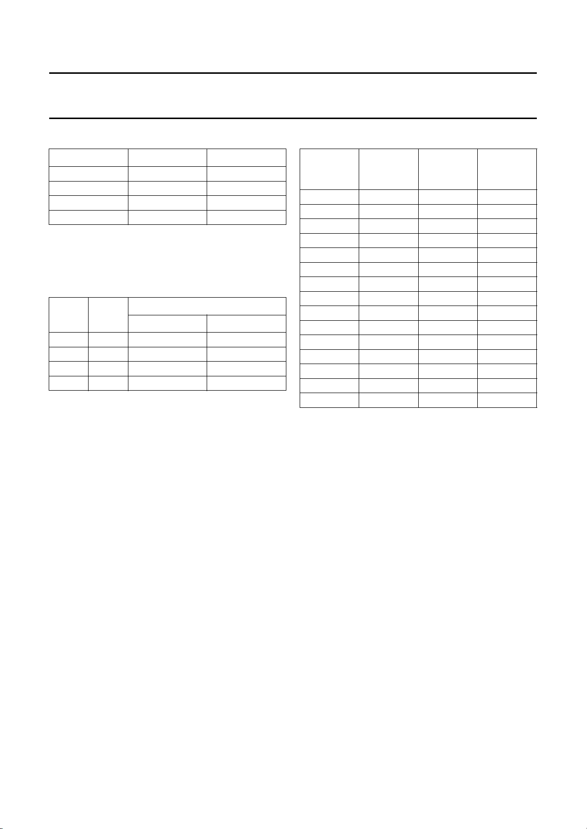
Table 4 Truth table for bits 21 and 20
B0 B1 BAND SELECT
00FM
(1)
01MW
10LW
11SW
Note
1. When FM is selected, the control output FM-ON/OFF
is set LOW to switch on the external FM front end.
Table 5 Truth table for bits 16 and 17
SIGNAL RECEPTION
(1)
S1 S0
FM IF INPUT AM RF INPUT
0 0 >50 µV >28 µV
0 1 >100 µV >40 µV
1 0 >300 µV >63 µV
1 1 >1500 µV >1000 µV
Note
1. The given values for signal reception are
corresponding to a −3 dB point of 20 µV for FM.
Table 6 Values for bits 14 to 0
BIT BIT VALUEFMVALUE
(kHz)
14 2
13 2
12 2
11 2
10 2
92
82
72
62
52
42
32
22
12
02
14
13
12
11
10
9
8
7
6
5
4
3
2
1
0
− 16384
102400 8192
51200 4096
25600 2048
12800 1024
6400 512
3200 256
1600 128
800 64
400 32
200 16
100 8
50 4
25 2
12.5 1
Notes
1. FM value of the affected oscillators;
FM VALUE = FM-RF + FM-IF.
2. AM value of the affected oscillators;
AM VALUE = AM-RF + AM-IF.
(1)
AM
VALUE
(kHz)
(2)
1995 Jun 23 9
Page 10

Philips Semiconductors Preliminary specification
Self tuned radio TEA5762
READING DATA
While write enable is LOW data can be read by the
microcontroller. At a rising edge of the bus-clock, data is
shifted out of the register. This data is available from the
point where the bus-clock is HIGH until the next rising
edge of the bus-clock occurs; see Fig.3
To read the entire shift register 24 clock pulses are
necessary.
handbook, full pagewidth
WRITE-ENABLE
BUS-CLOCK
DATA
data shiftdata available after search ready
MSB is LOW
WRITING DATA
While write enable is HIGH the microcontroller can
transmit data to the TEA5762 (hard mute is active). At a
rising edge of the bus-clock, the register shifts and accepts
one bit into LSB. At clock LOW the microcontroller writes
data; see Fig.4.
To write the entire shift register 25 clock pulses are
necessary.
data read
data available
MBE817
handbook, full pagewidth
WRITE-ENABLE
BUS-CLOCK
DATA
Fig.3 Read data.
MBE818
data changedata shift
Fig.4 Write data.
1995 Jun 23 10
Page 11
Philips Semiconductors Preliminary specification
Self tuned radio TEA5762
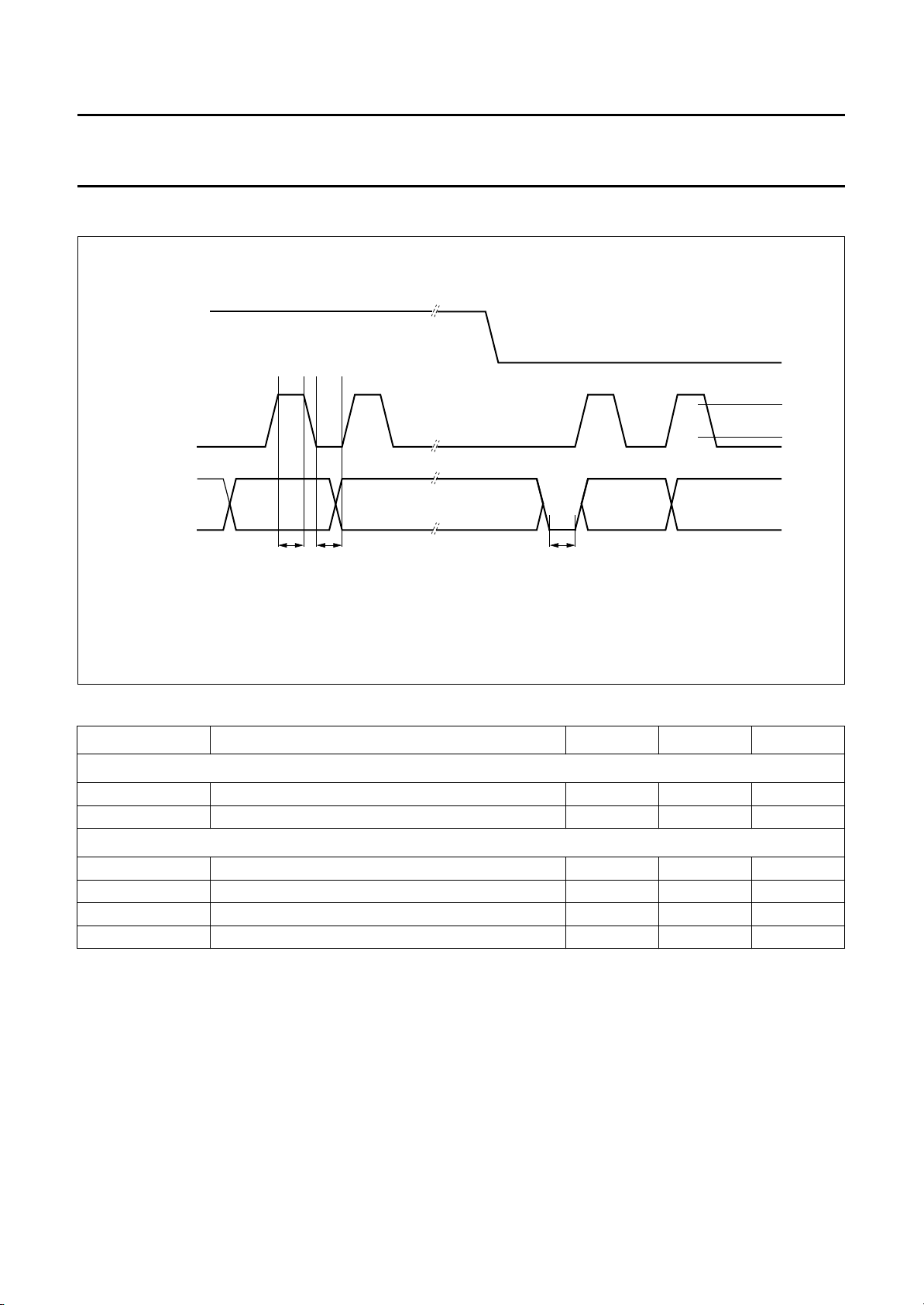
BUS TIMING
handbook, full pagewidth
WRITE-ENABLE
V
BUS-CLOCK
DATA
IH
V
IL
t
HIGHtLOW
t
da
Fig.5 Bus timing.
Table 7 Digital inputs
SYMBOL PARAMETER MIN. MAX. UNIT
Digital inputs
V
IH
V
IL
HIGH level input voltage 1.4 − V
LOW level input voltage − 0.6 V
Timing
f
clk
t
HIGH
t
LOW
t
da
clock input − 300 kHz
clock HIGH time 1.67 −µs
clock LOW time 1.67 −µs
shift register available after ‘search ready’ − 14 µs
MBE819
1995 Jun 23 11
Page 12
Philips Semiconductors Preliminary specification
Self tuned radio TEA5762
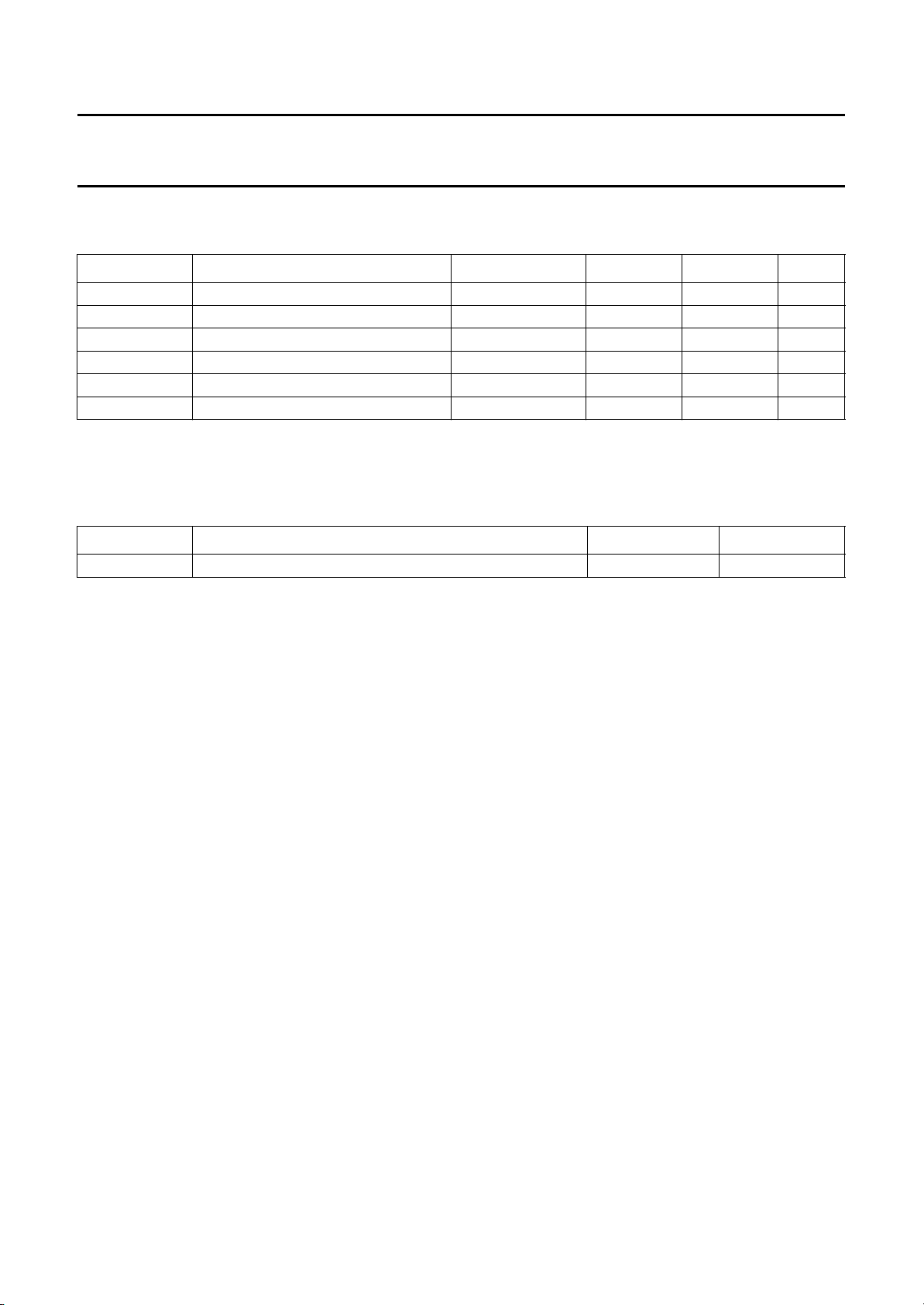
LIMITING VALUES
In accordance with the Absolute Maximum Rating System (IEC 134).
SYMBOL PARAMETER CONDITIONS MIN. MAX. UNIT
V
CC1
P
tot
T
stg
T
amb
T
j
V
es
Note
1. Charge device model: equivalent to discharging a 200 pF capacitor via a 0 Ω series resistor.
THERMAL CHARACTERISTICS
SYMBOL PARAMETER VALUE UNIT
R
th j-a
supply voltage 1 0 13.2 V
total power dissipation T
=70°C − 250 mW
amb
storage temperature −65 +150 °C
operating ambient temperature −15 +60 °C
operating junction temperature −15 +150 °C
electrostatic handling for all pins note 1 −±200 V
thermal resistance from junction to ambient in free air 65 K/W
1995 Jun 23 12
Page 13

Philips Semiconductors Preliminary specification
Self tuned radio TEA5762
CHARACTERISTICS
V
=3V; T
CC1
SYMBOL PARAMETER CONDITIONS MIN. TYP. MAX. UNIT
V
CC1
V
CC2
V
DDD
V
tune
I
CC2
f
clk(max)
I
CC1
I
DDD
I
CC1
I
DDD
t
search
t
acqu
f
band
∆f
FM
∆f
AM
I
P0/P1(sink)
I
P0/P1(source)
=25°C; unless otherwise specified.
amb
supply voltage 1 2.5 − 12 V
supply voltage 2 for tuning −−12 V
digital supply voltage 2.5 − 12 V
tuning voltage 0.7 − V
supply current 2 for tuning in preset mode
−−640 µA
CC2
− 0.75 V
(band-end to band-end)
maximum bus-clock frequency −−300 kHz
current consumption during acquisition of V
AM mode 12 15 18 mA
CC1
FM mode 12.5 15.5 18.5 mA
current consumption during acquisition of I
DDD
AM mode − 4.8 − mA
FM mode − 5.5 − mA
current consumption after acquisition of V
CC1
AM mode 12 15 18 mA
FM mode 13 16 19 mA
current consumption after acquisition of I
DDD
AM mode − 3.2 − mA
FM mode − 2.7 − mA
synthesizer auto-search time for empty band FM mode −−10 s
synthesizer preset acquisition time between two
band limits
FM − 100 − ms
MW − 150 − ms
LW − 1000 − ms
(1)
SW − 500
− ms
frequency band range of the synthesizer AM mode 0.144 − 30 MHz
AFC inaccuracy of FM with Mitsumi
−−1 kHz
front end
AFC inaccuracy of AM −−100 Hz
sink current of software programmable
V
=5V −−7mA
CC1
output P0/P1
source current of software programmable
V
=5V 5 − 7mA
CC1
output P0/P1
Note
1. Depending on band.
1995 Jun 23 13
Page 14

Philips Semiconductors Preliminary specification
Self tuned radio TEA5762
AM CHARACTERISTICS
Input frequency = 1 MHz; m = 0.3; f
Vi1measured at input of matching network at pin 2; matching network adjusted to maximum output voltage at low input
level; refer to test circuit (see Fig.8); unless otherwise specified.
SYMBOL PARAMETER CONDITIONS MIN. TYP. MAX. UNIT
V
10
V
i1
V
il
AF output voltage Vi1=5mV 364570mV
RF sensitivity input voltage S/N = 26 dB 40 55 70 µV
large signal voltage handling
capacity
PSSR power supply ripple rejection
/∆V7)
(V
10
I
i
C
i
G
c
input current (pin 2) V44= 0.2 V − 0 −µA
input capacitance (pin 2) V44= 0.2 V −−4pF
front end conversion gain V44= 0.2 V 5 10 14 dB
S/N signal-to-noise ratio − 50 − dB
THD total harmonic distortion V
α
450
IF suppression V10=30mV − 56 − dB
= 1 kHz; measured in test circuit at pin 10 (see Fig.8); S2 in position B;
mod
m = 0.8; THD ≤ 8% 150 300 − mV
∆V
= 100 mV (RMS);
7
100 Hz; V
= 0.9 V −26 −14 0 dB
V
44
=1mV − 0.8 2.0 %
i1
= 3.0 V
7
−−47 − dB
FM-IF CHARACTERISTICS
Input frequency = 10.7 MHz; ∆f = 22.5 kHz; f
= 1 kHz; measured in test circuit (see Fig.8) at pin 10; S2 in position B;
mod
refer to test circuit (see Fig.8); unless otherwise specified.
SYMBOL PARAMETER CONDITIONS MIN. TYP. MAX. UNIT
V
V
10
i4
AF output voltage Vi4=10mV 40 48 57 mV
IF limiting sensitivity V10= −3 dB; V10= 0 dB at
− 50 80 µV
Vi4=10mV
PSSR power supply ripple rejection
/∆V7)
(V
10
S/N signal-to-noise ratio V
∆V7= 100 mV (RMS);
100 Hz; V7= 3.0 V
=10mV 62 −−dB
i4
−44 −−dB
THD total harmonic distortion IF filter SFE10.7MS3A20K-A − 0.3 0.8 %
1995 Jun 23 14
Page 15
Philips Semiconductors Preliminary specification
Self tuned radio TEA5762
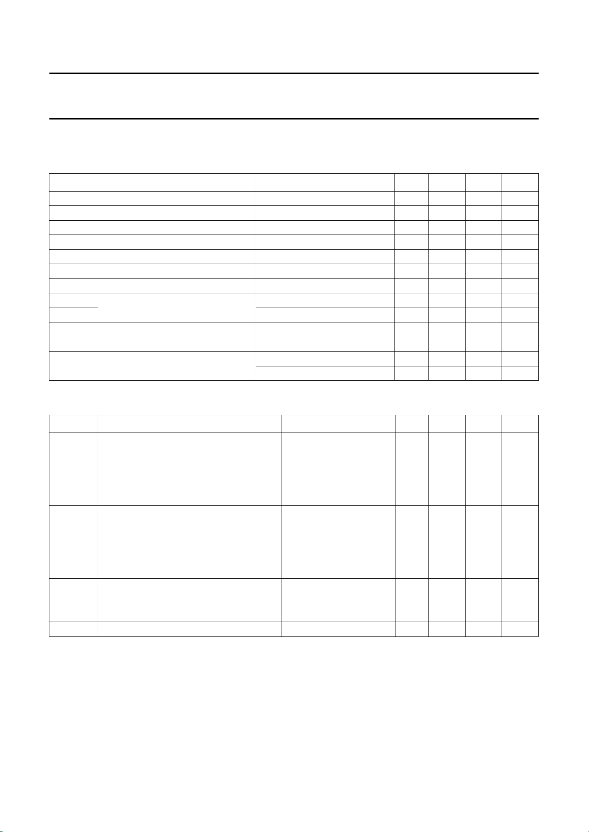
STEREO DECODER CHARACTERISTICS
V
maximum channel separation; soft mute off (S4 in position A); unless otherwise specified.
i3(L+R)
= 155 mV; V
= 15.5 mV; f = 1 kHz; apply unmodulated RF signal of 100 mV to front end to set radio to
pilot
SYMBOL PARAMETER CONDITIONS MIN. TYP. MAX. UNIT
V
14/15
V
pilot(s)
V
pilot(m)
V
AF-L/Vi3
S/N signal-to-noise ratio V
AF output voltage − 160 − mV
switch to stereo − 812mV
switch to mono 2 5 − mV
MPX voltage gain −1.5 − +1.5 dB
= 15.5 mV (stereo) − 74 − dB
pilot
THD total harmonic distortion − 0.5 1.0 %
α
cs
α
19
α
38
α stereo-blend V
mute(s) soft mute depth V
channel separation 26 30 − dB
carrier and harmonic suppression 19 kHz (200 mV)=0dB 27 32 − dB
38 kHz 16 21 − dB
=5mV 22 30 − dB
i4
= 200 µV − 12dB
V
i4
=30µV; V14=V
i4
=10µV; V14=V
V
i4
15
15
−10 − dB
−−6−10 dB
TUNING CHARACTERISTICS
SYMBOL PARAMETER CONDITIONS MIN. TYP. MAX. UNIT
V
FM
FM voltage levels α
-point at Vi4=20µV
−3dB
high (auto-store/search) S0 = 1; S1 = 1 600 1500 5000 µV
medium (auto-store/search) S0 = 0; S1 = 1 100 300 550 µV
low (auto-store/search) S0 = 1; S1 = 0 40 100 200 µV
nominal (preset mode/tuning indication) S0 = 0; S1 = 0 30 50 90 µV
V
AM
AM voltage levels α
-point at Vi4=20µV
−3dB
high (auto-store/search) S0 = 1; S1 = 1 400 1000 2500 µV
medium (auto-store/search) S0 = 0; S1 = 1 50 63 80 µV
low (auto-store/search) S0 = 1; S1 = 0 32 40 50 µV
nominal (preset mode/tuning indication) S0 = 0; S1 = 0 25 28 40 µV
V
AFC(off)
AFC voltage off mode α
-point at Vi4=20µV
−3dB
FM mode − 3 −µV
AM mode − 25 −µV
mute(h) hard mute write enable HIGH − 60 − dB
1995 Jun 23 15
Page 16
Philips Semiconductors Preliminary specification
Self tuned radio TEA5762
(%)
THD
8
9
120100806040200−20
(dBµV)
6
7
4
5
2
3
0
1
1
MBE853
(V)
i1
V
−1
10
−2
10
−3
10
(1)
(2)
(3)
−4
10
−5
10
−6
10
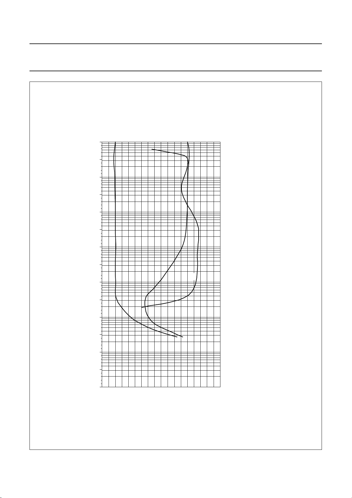
Fig.6 AM mode.
1995 Jun 23 16
0
10
(dB)
handbook, full pagewidth
−10
−7
−20
−30
−40
−50
−60
10
−70
−80
(1) Audio signal.
(2) Noise.
(3) Harmonic distortion.
Page 17
Philips Semiconductors Preliminary specification
Self tuned radio TEA5762
(%)
THD
8
9
120100806040200
(dBµV)
6
7
4
5
2
3
0
1
1
MBE854
(V)
i1
V
−1
10
−2
10
(3)
(4)
(5)
(6)
(7)
−3
10
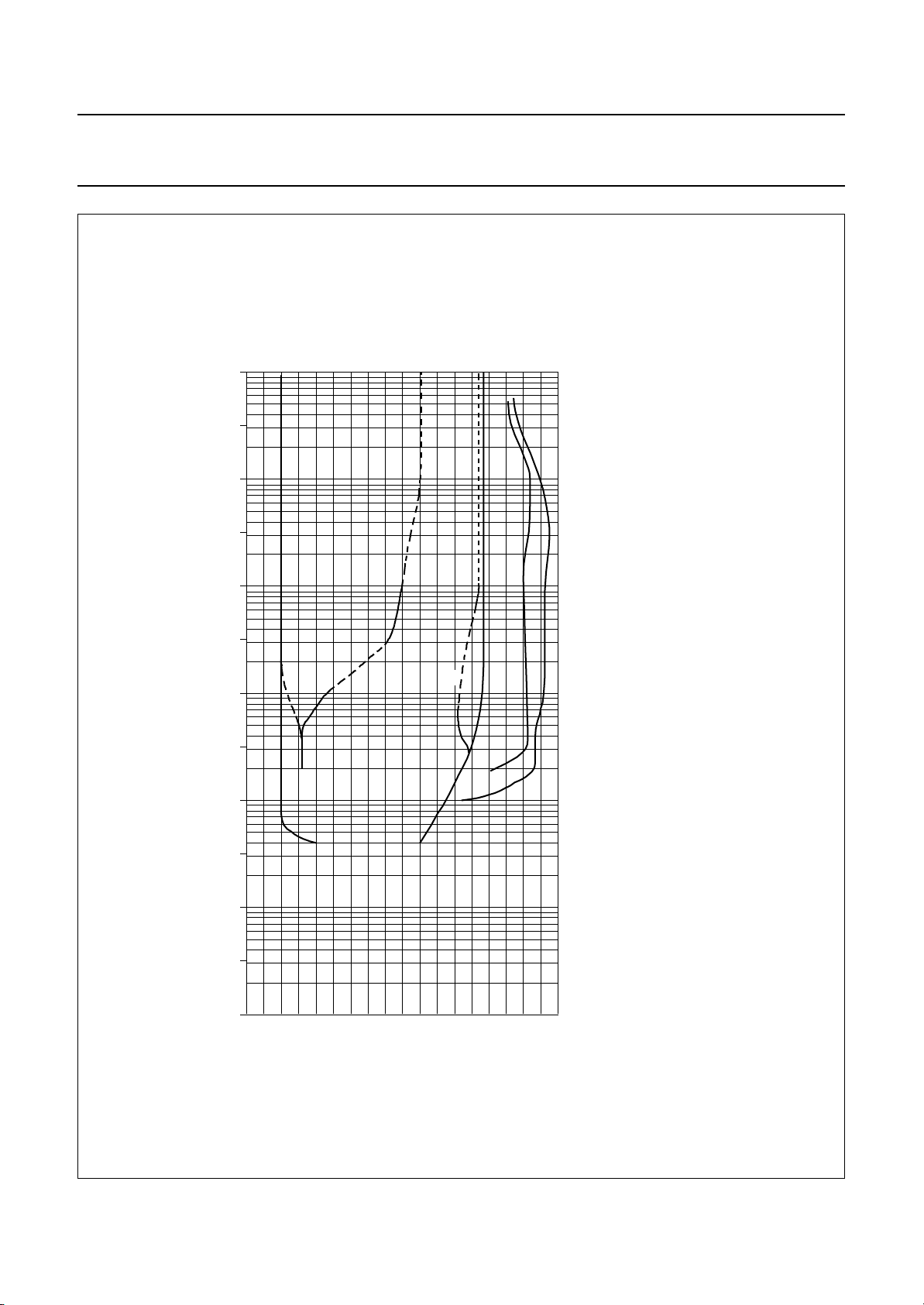
Fig.7 FM mode.
(1)
0
10
(dB)
−10
−20
−30
(2)
−40
−50
−60
−4
10
−5
10
−6
−70
10
−80
1995 Jun 23 17
handbook, full pagewidth
(1) Mono signal.
(2) Noise in mono mode.
(3) Left channel with modulation left.
(4) Right channel with modulation left.
(5) Noise in stereo mode.
(6) Harmonic distortion ∆f = 75 kHz.
(7) Total harmonic distortion ∆f = 22.5 kHz.
Page 18
Philips Semiconductors Preliminary specification
Self tuned radio TEA5762
INTERNAL CIRCUITS
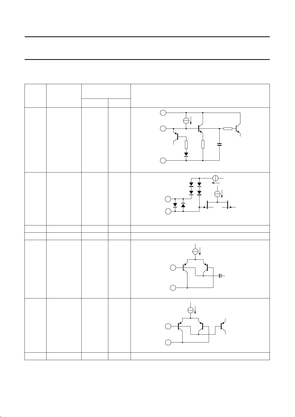
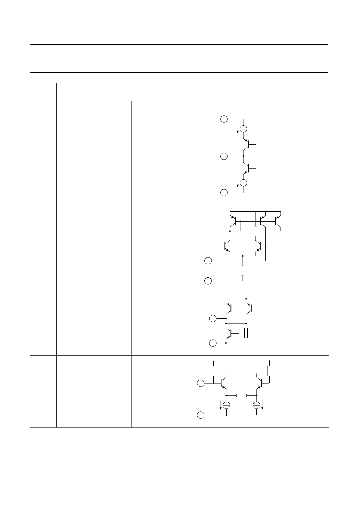
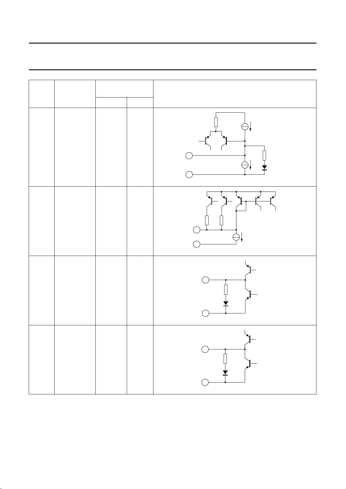
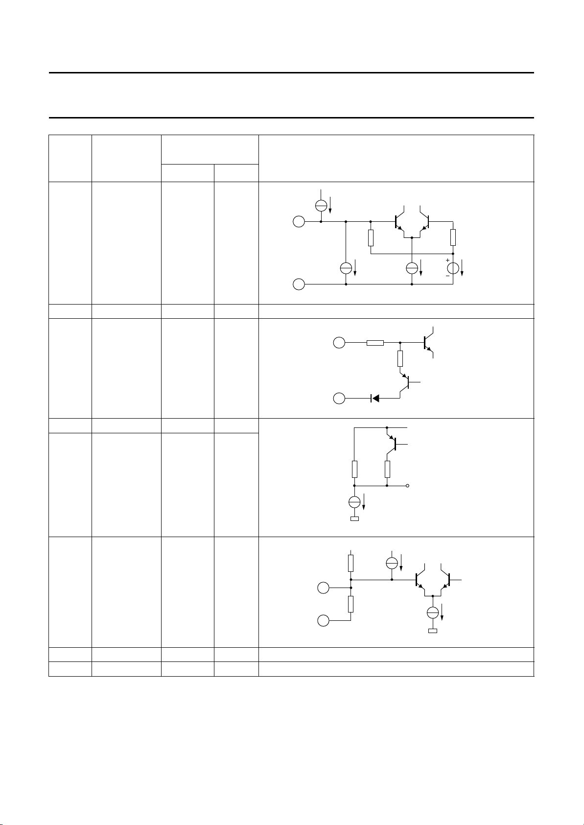
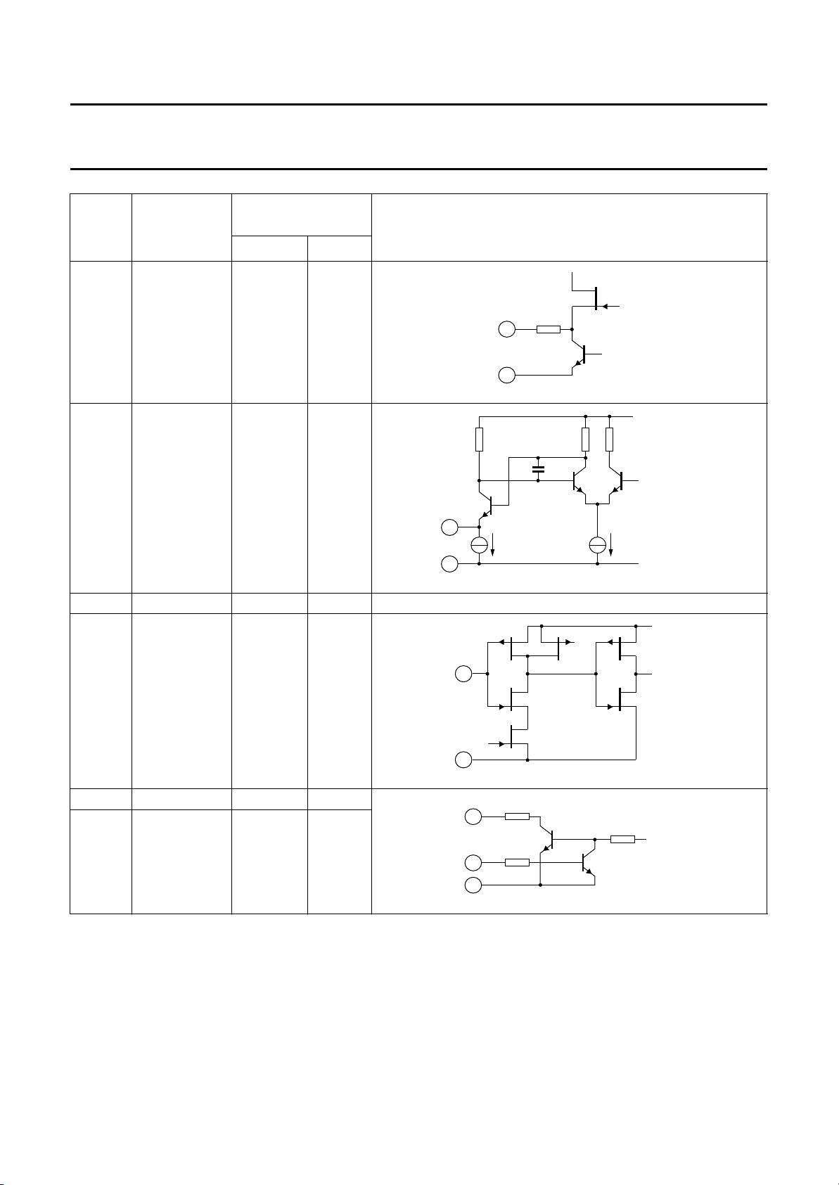
Table 8 Equivalent pin circuits and pin voltages
DC VOLTAGE
PIN SYMBOL
1 RIPPLE 2.1 2.1
(V)
AM FM
EQUIVALENT CIRCUIT
7
2 AM-RFI 0 0
3 RFGND1 −−
4 CGND 0 0
5 COUNTI 0 0
17
1
3 kΩ
4
2
5
1 kΩ
70 pF
MBE821
MBE822
6 AMOSC 0 0
7V
CC1
1995 Jun 23 18
3.0 3.0
4
6
4
MBE823
MBE824
Page 19
Philips Semiconductors Preliminary specification
Self tuned radio TEA5762
DC VOLTAGE
PIN SYMBOL
8 TUNE −−
(V)
AM FM
EQUIVALENT CIRCUIT
22
8
9 VCO 1.3 0.95
10 AFO 0.6 0.7
11 MPXI 1.23 1.23
26
9
17
10
17
150 kΩ 150 kΩ
MBE825
1 kΩ
10 kΩ
5 kΩ
MBE826
MBE827
1995 Jun 23 19
11
9.5 kΩ
17
MBE828
Page 20
Philips Semiconductors Preliminary specification
Self tuned radio TEA5762
DC VOLTAGE
PIN SYMBOL
12 LFI 0.1 0.8
(V)
AM FM
EQUIVALENT CIRCUIT
4 kΩ
13 MUTE 0.7 0.7
14 AFLO 0.65 0.65
12
17
7 kΩ 50 kΩ
13
17
14
5 kΩ
17
13 kΩ
MBE829
MBE830
MBE831
15 AFRO 0.65 0.65
1995 Jun 23 20
15
5 kΩ
17
MBE832
Page 21
Philips Semiconductors Preliminary specification
Self tuned radio TEA5762
DC VOLTAGE
PIN SYMBOL
16 PILFIL 0.95 0.95
(V)
AM FM
EQUIVALENT CIRCUIT
16
10 kΩ
10 kΩ
17 IFGND 0 0
18 FMDEM − 1.0
19 AFC
20 AFC
(n)
(p)
−−
−−
21 FSI −−
17
18
17
1.4 V
180 Ω
910 Ω
MBE834
10 kΩ 10 kΩ
19/20
MBE835
40 kΩ
MBE833
22 V
23 V
CC2
DDD
1995 Jun 23 21
21
12 to 34 kΩ
(dependent on
bits 16 and 17)
26
MBE836
−−
3.0 3.0
Page 22
Philips Semiconductors Preliminary specification
Self tuned radio TEA5762
DC VOLTAGE
PIN SYMBOL
24 MO/ST −−
(V)
AM FM
EQUIVALENT CIRCUIT
100 Ω
24
25 XTAL −−
26 DGND 0 0
27 BUS-CLOCK −−
26
25
26
27
26
MBE837
50 kΩ50 kΩ50 kΩ
MBE838
MBE839
28 DATA −−
29 WRITE-
ENABLE
1995 Jun 23 22
−−
100 Ω
28
50 kΩ
29
26
100 kΩ
MBE840
Page 23
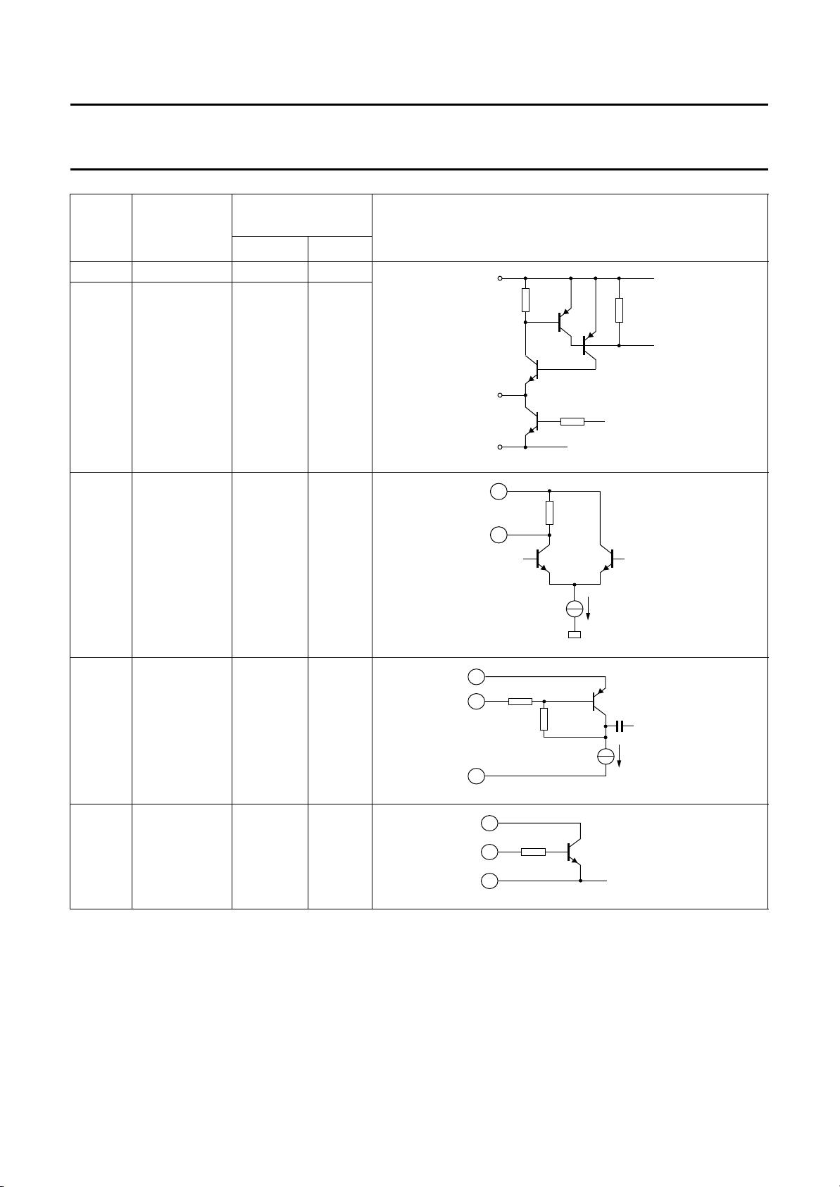
Philips Semiconductors Preliminary specification
Self tuned radio TEA5762
DC VOLTAGE
PIN SYMBOL
30 P0 −−
31 P1 −−
(V)
AM FM
EQUIVALENT CIRCUIT
23
120 kΩ
30/31
20 kΩ
100 kΩ
32 AFC −−
33 FM-IF2I − 0.73
34 V
STAB(B)
1.4 1.4
26
34
20 kΩ
32
34
140 Ω
33
2.2 kΩ
17
7
1 kΩ
1
MBE841
MBE842
6 pF
MBE843
1995 Jun 23 23
34
MBE844
Page 24
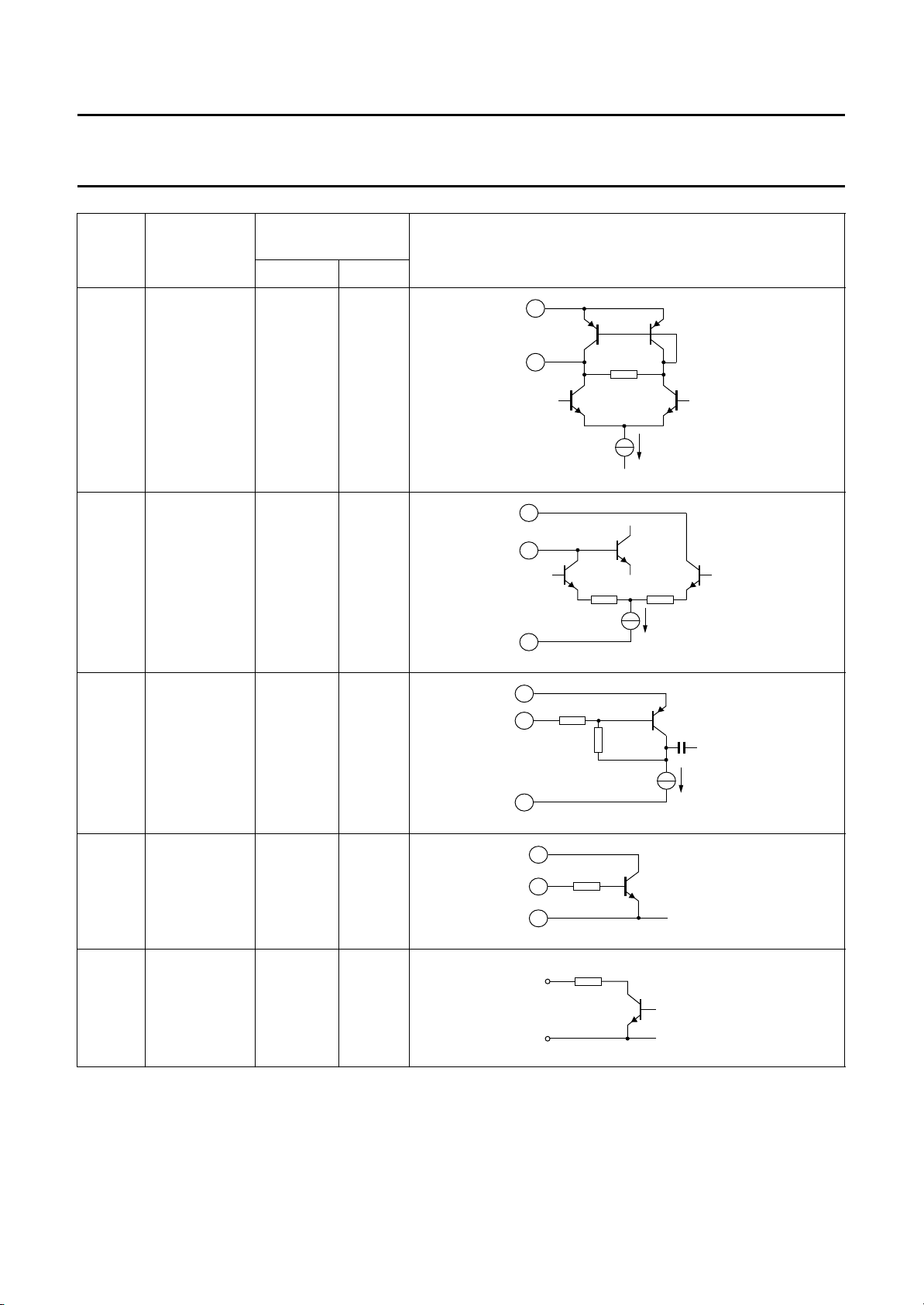
Philips Semiconductors Preliminary specification
Self tuned radio TEA5762
DC VOLTAGE
PIN SYMBOL
35 FM-IFO1 − 0.69
(V)
AM FM
EQUIVALENT CIRCUIT
34
36 AM-IF2I/O 1.4 1.4
37 FM-IFI1 − 0.73
35
34
36
17
38
140 Ω
37
17
560 Ω
3.6 kΩ 3.6 kΩ
1.9 kΩ
MBE845
MBE846
6 pF
MBE847
38 V
STAB(A)
1.4 1.4
39 FM-ON/OFF −−
1995 Jun 23 24
7
1 kΩ
1
38
500 Ω
39
26
MBE848
MBE849
Page 25
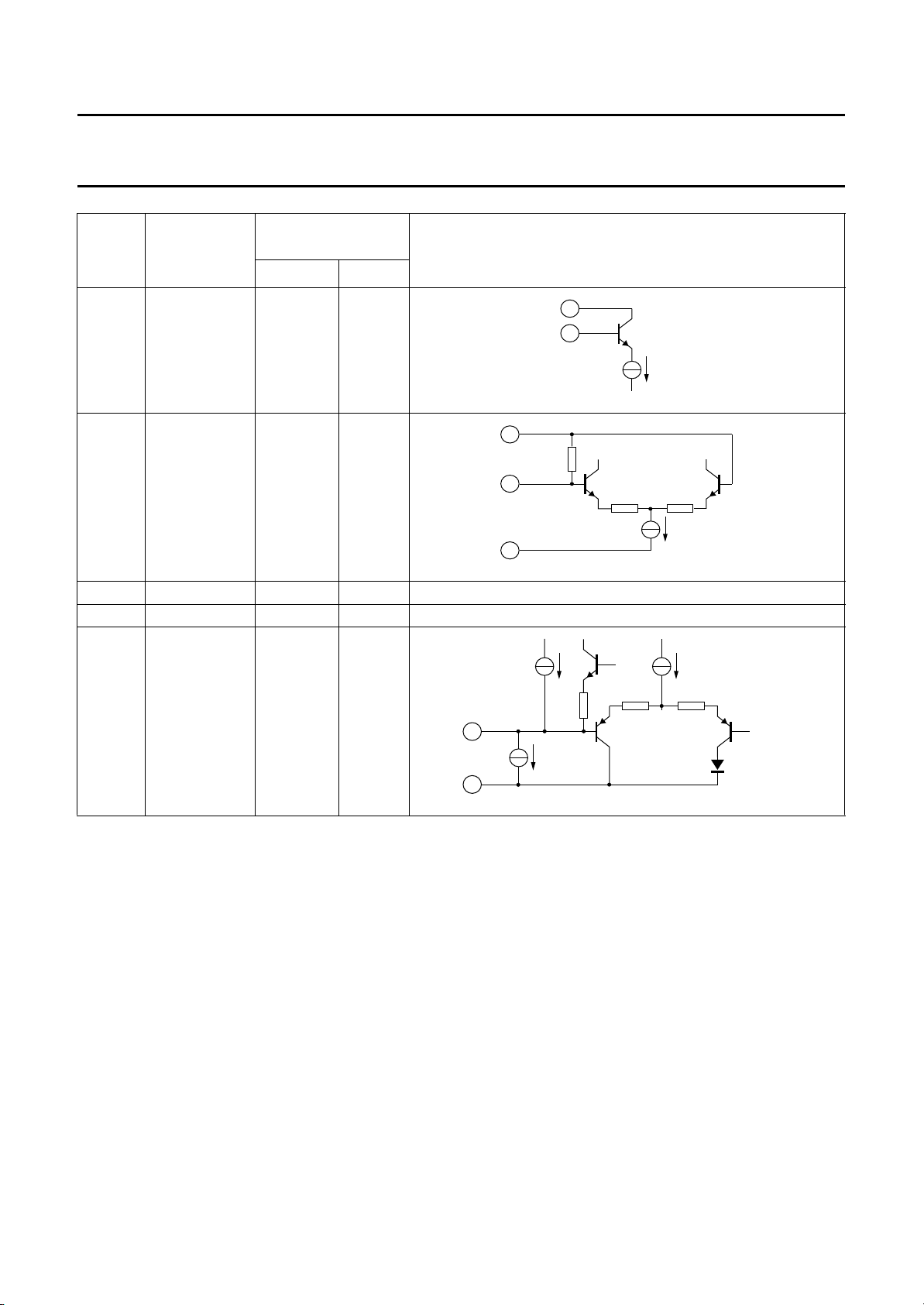
Philips Semiconductors Preliminary specification
Self tuned radio TEA5762
DC VOLTAGE
PIN SYMBOL
40 AM-MIXER 1.4 1.4
(V)
AM FM
EQUIVALENT CIRCUIT
40
38
MBE850
41 AM-IF1I 1.4 1.4
42 RFGND2 0 0
43 n.c. −−
44 AGC 0.1 0.7
38
3 kΩ
41
17
1 kΩ
44
17
7.5 kΩ
1 kΩ
7.5 kΩ
MBE851
1 kΩ
MBE852
1995 Jun 23 25
Page 26
Philips Semiconductors Preliminary specification
Self tuned radio TEA5762
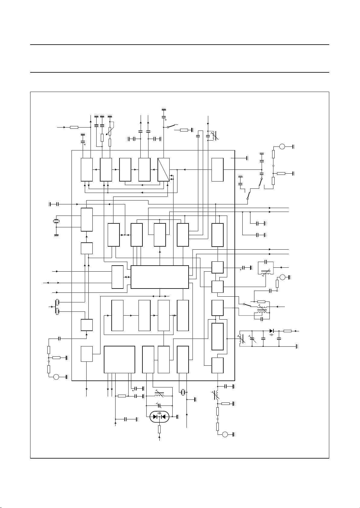
TEST AND APPLICATION INFORMATION
DATA
(8)
K2
BUS-
CLOCK
WRITE-
ENABLE
STAB(B)
V
330 Ω
i4
V
50 Ω
CC1
V
100 nF
K1
(7)
1 nF
50 Ω
10.7 MHz
10 kΩ
21
1817272829333537
2.2 µF
16
MO/ST
470 nF
24
PILOT
DETECTOR
19 kHz
FM
DETECTOR
FM
IF2
FM
IF1
TUNER
SWITCH
39
FM-ON/OFF
2.2 kΩ
12
470 nF
50 kΩ
68 kΩ
9
PLL
38 kHz
AM/FM
INDICATOR
STATUS
38
34
7
STAB(A)VSTAB(B)
V
CC1
V
100 nF
12 nF
14
stereo
DECODER
IN-LOCK
DETECTOR
up
down
REGISTER
SHIFT REGISTER
STABILIZER
µF
100
10 Ω
220 nF
100 nF
AFLO
AFRO
100 nF
12 nF
15
mono
MATRIX
stereo
level
FM
MEMORY
LAST-STATION
PRESCALER
5231
4
10
18 kΩ
4.7 µF
S4
BA
13
MUTE
SDS
PUMP
hard mute level
CHARGE
CIRCUIT
SEQUENTIAL
AM
COUNTER
PROGRAMMABLE
MULTIPLEXER
(6)
L6
pF
BB204
TUNE
8.2 kΩ
AFC
WINDOW
CRYSTAL
25
75 kHz
470 nF
20
19
TDA5762
DETECTOR
OSCILLATOR
26
DGND
STAB(B)
V
32
(1)
(5)
L5
V/I
AM
AGC
AM
AM
AM
AM
FRONT
2
L1
i1
V
50 Ω 43 Ω
CONVERTER
10 11 3
DETECTOR
IF
MIXER
6404136443130822
OSCILLATOR
END
680 pF
6.8 Ω
1 MHz
MBE814
MPXI
50 Ω
330 pF
i3
V
50 Ω
220 nF
S3
S2
A
B
(2)
A
470 nF 10 nF
(4)
10 µF
B
A
S1
L2
18 pF
18 pF
B
L4
220 µF
3 kΩ
(3)
L3
BB112
(1) L1 = 22281-30091.
(2) L2 = A7BRS-12287Y.
(3) L3 = A7MCS-11844N.
5 kΩ
CC2
V
P0 TUNEP1
STAB(B)
V
50 Ω
450 kHz
i2
V
STAB(A)
V
47 kΩ
470 pF
(4) L4 = A7MCS-11845Y.
(5) L5 = A7MCS-11845Y.
(6) L6 = S18 301SS-0200.
handbook, full pagewidth
Fig.8 Test circuit.
TUNE
(7) K1 = SFT10.7MS3.
(8) K2 = CDA10.7MC40-A.
1995 Jun 23 26
Page 27
Philips Semiconductors Preliminary specification
Self tuned radio TEA5762
APPLICATION INFORMATION
AFLO
V
CC1
MO/ST
10 kΩ
470 nF
2.2 µF
24
16
470 nF
50 kΩ
2.2 kΩ
68 kΩ
9
12
12 nF
100 nF
14
AFRO
100 nF
15
12 nF
13
4.7 µF
470 nF
19
STAB(B)
V
(5)
L5
32
20
MBE816
STAB(A)
V
10 µF
(2)
220 nF
(3)
L2
330 pF
10 nF
470 nF
(4)
L3
18 pF
CC2
V
TUNE
P0
P1
L4
BB112
STAB(B)
V
STAB(A)
V
47 kΩ
handbook, full pagewidth
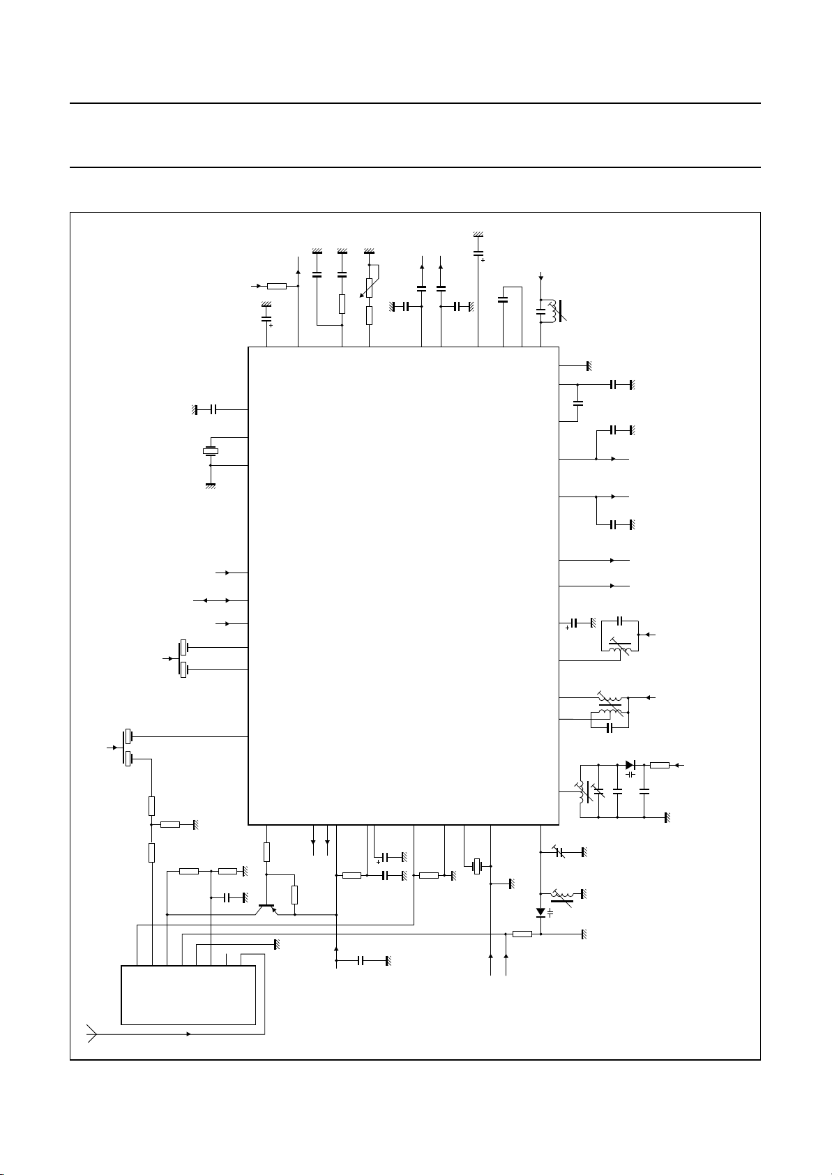
Fig.9 Application circuit.
TUNE
11 3
100 nF
21
CLOCK
WRITE-
ENABLE
1817
2728293335
TEA5762
37
(8)
K3
BUS-
DATA
STAB(B)
V
K2
(7)
K1
(6)
10
6404136443130822
150 Ω
220 Ω
150 Ω
CC
V
TUNE
IF-OUT
OSC-OUT
FM-Front end
Mitsumi FE415-G11
V
1995 Jun 23 27
470 pF
18 pF
7
CC1
10 Ω
23
100 nF
1
100
µF
220 nF
38
68 kΩ
34
STAB(A)VSTAB(B)
V
V
39
470
n.c.
10 kΩ
150 kΩ
pF
ANT
220 kΩ
AGC
GND
4
5
25
26
120 Ω
75 kHz
GND
TUNE
BB112
47 kΩ
2
22 nF
18 pF
(1)
L1
(1) L1 = 250 µH ferroceptor.
(2) L2 = A7BRS-12287Y.
(3) L3 = A7MCS-11844N.
(4) L5 = A7MCS-11845Y.
(5) L4 = A7MCS-11845Y.
(6) K1 = SFT10.7MS3.
(7) K2 = SFT10.7MS3.
(8) K3 = CDA10.7MC40-A.
Page 28
Philips Semiconductors Preliminary specification
Self tuned radio TEA5762
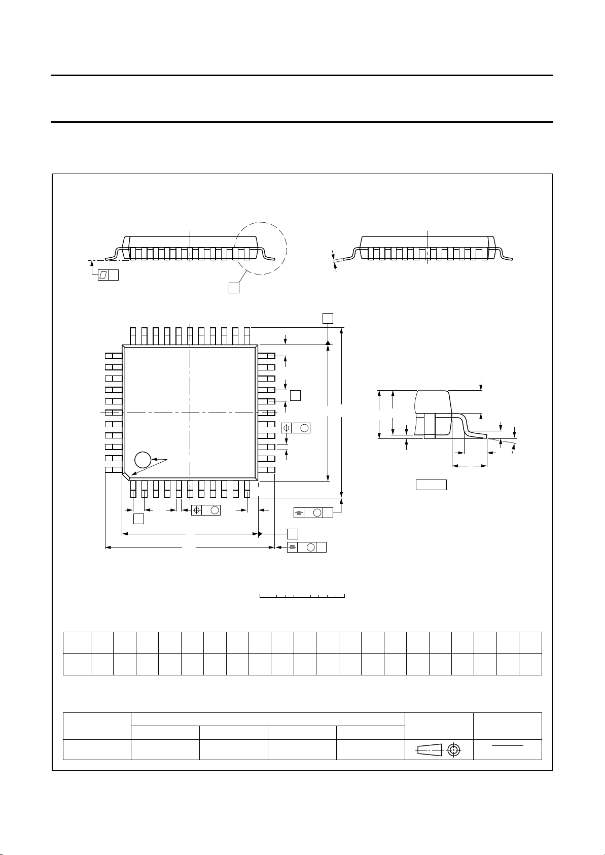
PACKAGE OUTLINE
QFP44: plastic quad flat package; 44 leads (lead length 1.3 mm); body 10 x 10 x 1.75 mm
c
y
X
A
33 23
34
pin 1 index
44
1
22
Z
E
e
H
E
E
w M
b
p
12
11
A
2
A
A
1
detail X
SOT307-2
Q
(A )
3
θ
L
p
L
w M
b
e
DIMENSIONS (mm are the original dimensions)
mm
OUTLINE
VERSION
SOT307-2
A
max.
2.10
0.25
0.05
1.85
1.65
UNIT A1A2A3b
Note
1. Plastic or metal protrusions of 0.25 mm maximum per side are not included.
p
D
H
D
cE
p
0.40
0.20
0.25
0.14
0.25
IEC JEDEC EIAJ
Z
D
B
0 2.5 5 mm
scale
(1)
(1) (1)(1)
D
10.1
9.9
REFERENCES
eH
10.1
9.9
12.9
0.8 1.3
12.3
1995 Jun 23 28
v M
H
v M
D
A
B
LLpQZywv θ
E
12.9
12.3
0.95
0.55
0.85
0.75
0.15 0.10.15
EUROPEAN
PROJECTION
Z
D
1.2
1.2
0.8
0.8
ISSUE DATE
92-11-17
95-02-04
E
o
10
o
0
Page 29

Philips Semiconductors Preliminary specification
Self tuned radio TEA5762
SOLDERING QFP or SO
Introduction
There is no soldering method that is ideal for all IC
packages. Wave soldering is often preferred when
through-hole and surface mounted components are mixed
on one printed-circuit board. However, wave soldering is
not always suitable for surface mounted ICs, or for
printed-circuits with high population densities. In these
cases reflow soldering is often used.
This text gives a very brief insight to a complex technology.
A more in-depth account of soldering ICs can be found in
our
“IC Package Databook”
Reflow soldering
Reflow soldering techniques are suitable for all QFP and
SO packages.
The choice of heating method may be influenced by larger
plastic QFP packages (44 leads, or more). If infrared or
vapour phase heating is used and the large packages are
not absolutely dry (less than 0.1% moisture content by
weight), vaporization of the small amount of moisture in
them can cause cracking of the plastic body. For more
information, refer to the Drypack chapter in our
Reference Manual”
Reflow soldering requires solder paste (a suspension of
fine solder particles, flux and binding agent) to be applied
to the printed-circuit board by screen printing, stencilling or
pressure-syringe dispensing before package placement.
Several techniques exist for reflowing; for example,
thermal conduction by heated belt. Dwell times vary
between 50 and 300 seconds depending on heating
method. Typical reflow temperatures range from
215 to 250 °C.
Preheating is necessary to dry the paste and evaporate
the binding agent. Preheating duration: 45 minutes at
45 °C.
(order code 9398 510 63011).
(order code 9398 652 90011).
“Quality
If wave soldering cannot be avoided, the following
conditions must be observed:
• A double-wave (a turbulent wave with high upward
pressure followed by a smooth laminar wave)
soldering technique should be used.
• The footprint must be at an angle of 45° to the board
direction and must incorporate solder thieves
downstream and at the side corners.
Even with these conditions, do not consider wave
soldering the following packages: QFP52 (SOT379-1),
QFP100 (SOT317-1), QFP100 (SOT317-2),
QFP100 (SOT382-1) or QFP160 (SOT322-1).
SO
Wave soldering techniques can be used for all SO
packages if the following conditions are observed:
• A double-wave (a turbulent wave with high upward
pressure followed by a smooth laminar wave) soldering
technique should be used.
• The longitudinal axis of the package footprint must be
parallel to the solder flow.
• The package footprint must incorporate solder thieves at
the downstream end.
ETHOD (QFP OR SO)
M
During placement and before soldering, the package must
be fixed with a droplet of adhesive. The adhesive can be
applied by screen printing, pin transfer or syringe
dispensing. The package can be soldered after the
adhesive is cured.
Maximum permissible solder temperature is 260 °C, and
maximum duration of package immersion in solder is
10 seconds, if cooled to less than 150 °C within
6 seconds. Typical dwell time is 4 seconds at 250 °C.
A mildly-activated flux will eliminate the need for removal
of corrosive residues in most applications.
Wave soldering
QFP
Wave soldering is not recommended for QFP packages.
This is because of the likelihood of solder bridging due to
closely-spaced leads and the possibility of incomplete
solder penetration in multi-lead devices.
1995 Jun 23 29
Repairing soldered joints
Fix the component by first soldering two diagonallyopposite end leads. Use only a low voltage soldering iron
(less than 24 V) applied to the flat part of the lead. Contact
time must be limited to 10 seconds at up to 300 °C. When
using a dedicated tool, all other leads can be soldered in
one operation within 2 to 5 seconds at 270 to 320 °C.
Page 30

Philips Semiconductors Preliminary specification
Self tuned radio TEA5762
DEFINITIONS
Data sheet status
Objective specification This data sheet contains target or goal specifications for product development.
Preliminary specification This data sheet contains preliminary data; supplementary data may be published later.
Product specification This data sheet contains final product specifications.
Limiting values
Limiting values given are in accordance with the Absolute Maximum Rating System (IEC 134). Stress above one or
more of the limiting values may cause permanent damage to the device. These are stress ratings only and operation
of the device at these or at any other conditions above those given in the Characteristics sections of the specification
is not implied. Exposure to limiting values for extended periods may affect device reliability.
Application information
Where application information is given, it is advisory and does not form part of the specification.
LIFE SUPPORT APPLICATIONS
These products are not designed for use in life support appliances, devices, or systems where malfunction of these
products can reasonably be expected to result in personal injury. Philips customers using or selling these products for
use in such applications do so at their own risk and agree to fully indemnify Philips for any damages resulting from such
improper use or sale.
1995 Jun 23 30
Page 31

Philips Semiconductors Preliminary specification
Self tuned radio TEA5762
NOTES
1995 Jun 23 31
Page 32

Philips Semiconductors – a worldwide company
Argentina: IEROD, Av. Juramento 1992 - 14.b, (1428)
BUENOS AIRES, Tel. (541)786 7633, Fax. (541)786 9367
Australia: 34 Waterloo Road, NORTH RYDE, NSW 2113,
Tel. (02)805 4455, Fax. (02)805 4466
Austria: Triester Str. 64, A-1101 WIEN, P.O. Box 213,
Tel. (01)60 101-1236, Fax. (01)60 101-1211
Belgium: Postbus 90050, 5600 PB EINDHOVEN, The Netherlands,
Tel. (31)40 783 749, Fax. (31)40 788 399
Brazil: Rua do Rocio 220 - 5
CEP: 04552-903-SÃO PAULO-SP, Brazil.
P.O. Box 7383 (01064-970),
Tel. (011)821-2333, Fax. (011)829-1849
Canada: PHILIPS SEMICONDUCTORS/COMPONENTS:
Tel. (800) 234-7381, Fax. (708) 296-8556
Chile: Av. Santa Maria 0760, SANTIAGO,
Tel. (02)773 816, Fax. (02)777 6730
Colombia: IPRELENSO LTDA, Carrera 21 No. 56-17,
77621 BOGOTA, Tel. (571)249 7624/(571)217 4609,
Fax. (571)217 4549
Denmark: Prags Boulevard 80, PB 1919, DK-2300
COPENHAGEN S, Tel. (032)88 2636, Fax. (031)57 1949
Finland: Sinikalliontie 3, FIN-02630 ESPOO,
Tel. (358)0-615 800, Fax. (358)0-61580 920
France: 4 Rue du Port-aux-Vins, BP317,
92156 SURESNES Cedex,
Tel. (01)4099 6161, Fax. (01)4099 6427
Germany: P.O. Box 10 63 23, 20043 HAMBURG,
Tel. (040)3296-0, Fax. (040)3296 213.
Greece: No. 15, 25th March Street, GR 17778 TAVROS,
Tel. (01)4894 339/4894 911, Fax. (01)4814 240
Hong Kong: PHILIPS HONG KONG Ltd., 15/F Philips Ind. Bldg.,
24-28 Kung Yip St., KWAI CHUNG, N.T.,
Tel. (852)424 5121, Fax. (852)480 6960/480 6009
India: Philips INDIA Ltd, Shivsagar Estate, A Block ,
Dr. Annie Besant Rd. Worli, Bombay 400 018
Tel. (022)4938 541, Fax. (022)4938 722
Indonesia: Philips House, Jalan H.R. Rasuna Said Kav. 3-4,
P.O. Box 4252, JAKARTA 12950,
Tel. (021)5201 122, Fax. (021)5205 189
Ireland: Newstead, Clonskeagh, DUBLIN 14,
Tel. (01)7640 000, Fax. (01)7640 200
Italy: PHILIPS SEMICONDUCTORS S.r.l.,
Piazza IV Novembre 3, 20124 MILANO,
Tel. (0039)2 6752 2531, Fax. (0039)2 6752 2557
Japan: Philips Bldg13-37, Kohnan 2-chome, Minato-ku, TOKYO 108,
Tel. (03)3740 5130, Fax. (03)3740 5077
Korea: Philips House, 260-199 Itaewon-dong,
Yongsan-ku, SEOUL, Tel. (02)709-1412, Fax. (02)709-1415
Malaysia: No. 76 Jalan Universiti, 46200 PETALING JAYA,
SELANGOR, Tel. (03)750 5214, Fax. (03)757 4880
Mexico: 5900 Gateway East, Suite 200, EL PASO, TX 79905,
Tel. 9-5(800)234-7381, Fax. (708)296-8556
Netherlands: Postbus 90050, 5600 PB EINDHOVEN, Bldg. VB
Tel. (040)783749, Fax. (040)788399
New Zealand: 2 Wagener Place, C.P.O. Box 1041, AUCKLAND,
Tel. (09)849-4160, Fax. (09)849-7811
Norway: Box 1, Manglerud 0612, OSLO,
Tel. (022)74 8000, Fax. (022)74 8341
th
floor, Suite 51,
Pakistan: Philips Electrical Industries of Pakistan Ltd.,
Exchange Bldg. ST-2/A, Block 9, KDA Scheme 5, Clifton,
KARACHI 75600, Tel. (021)587 4641-49,
Fax. (021)577035/5874546
Philippines: PHILIPS SEMICONDUCTORS PHILIPPINES Inc,
106 Valero St. Salcedo Village, P.O. Box 2108 MCC, MAKATI,
Metro MANILA, Tel. (02)810 0161, Fax. (02)817 3474
Portugal: PHILIPS PORTUGUESA, S.A.,
Rua dr. António Loureiro Borges 5, Arquiparque - Miraflores,
Apartado 300, 2795 LINDA-A-VELHA,
Tel. (01)4163160/4163333, Fax. (01)4163174/4163366
Singapore: Lorong 1, Toa Payoh, SINGAPORE 1231,
Tel. (65)350 2000, Fax. (65)251 6500
South Africa: S.A. PHILIPS Pty Ltd.,
195-215 Main Road Martindale, 2092 JOHANNESBURG,
P.O. Box 7430, Johannesburg 2000,
Tel. (011)470-5911, Fax. (011)470-5494.
Spain: Balmes 22, 08007 BARCELONA,
Tel. (03)301 6312, Fax. (03)301 42 43
Sweden: Kottbygatan 7, Akalla. S-164 85 STOCKHOLM,
Tel. (0)8-632 2000, Fax. (0)8-632 2745
Switzerland: Allmendstrasse 140, CH-8027 ZÜRICH,
Tel. (01)488 2211, Fax. (01)481 77 30
Taiwan: PHILIPS TAIWAN Ltd., 23-30F, 66, Chung Hsiao West
Road, Sec. 1. Taipeh, Taiwan ROC, P.O. Box 22978,
TAIPEI 100, Tel. (02)388 7666, Fax. (02)382 4382
Thailand: PHILIPS ELECTRONICS (THAILAND) Ltd.,
209/2 Sanpavuth-Bangna Road Prakanong,
Bangkok 10260, THAILAND,
Tel. (662)398-0141, Fax. (662)398-3319
Turkey:Talatpasa Cad. No. 5, 80640 GÜLTEPE/ISTANBUL,
Tel. (0212)279 27 70, Fax. (0212)282 67 07
United Kingdom: Philips Semiconductors LTD.,
276 Bath Road, Hayes, MIDDLESEX UB3 5BX,
Tel. (0181)730-5000, Fax. (0181)754-8421
United States:811 East Arques Avenue, SUNNYVALE,
CA 94088-3409, Tel. (800)234-7381, Fax. (708)296-8556
Uruguay: Coronel Mora 433, MONTEVIDEO,
Tel. (02)70-4044, Fax. (02)92 0601
Internet: http://www.semiconductors.philips.com/ps/
For all other countries apply to: Philips Semiconductors,
International Marketing and Sales, Building BE-p,
P.O. Box 218, 5600 MD EINDHOVEN, The Netherlands,
Telex 35000 phtcnl, Fax. +31-40-724825
SCD40 © Philips Electronics N.V. 1995
All rights are reserved. Reproduction in whole or in part is prohibited without the
prior written consent of the copyright owner.
The information presented in this document does not form part of any quotation
or contract, is believed to be accurate and reliable and may be changed without
notice. No liability will be accepted by the publisher for any consequence of its
use. Publication thereof does not convey nor imply any license under patent- or
other industrial or intellectual property rights.
Printed in The Netherlands
533061/1500/01/pp32 Date of release: 1995 Jun 23
Document order number: 9397 750 00178
 Loading...