

Page 1

INTEGRATED CIRCUITS
DATA SH EET
TEA1069; TEA1069A
Versatile speech/dialler/ringer with
music-on-hold
Product specification
Supersedes data of 1996 Dec 10
File under Integrated Circuits, IC03
1998 Jan 08
Page 2

Philips Semiconductors Product specification
Versatile speech/dialler/ringer with
music-on-hold
FEATURES
Speech part
• Voltage regulator with adjustable static resistance
• Low DC line voltage; operates down to 1.6 V
(excluding polarity guard)
• Supply for dialler part and peripherals (not stabilized)
• Symmetrical high-impedance inputs (64 kΩ) for
dynamic, magnetic, or piezoelectric microphones
• Asymmetrical high-impedance input (32 kΩ) for electret
microphones
• Asymmetrical earpiece output for dynamic, magnetic,
or piezoelectric earpieces
• Internal mute to disable speech during dialling
• Confidence tone during DTMF dialling
• Line-loss compensation (line-current dependent) for
microphone and earpiece amplifiers
• Gain-control curve adaptable to the exchange supply.
Dialler part
• Pulse/DTMF and mixed mode dialling
• Last Number Redial (LNR), up to 32 digits
• 13 repertory numbers (3 direct and 10 indirect) or
10 repertory numbers (10 direct), up to 32 digits,
with a maximum of 224 digits in total
• Repertory and redial memory integrity check
(memory contents check)
• Notepad memory function
• Flash and earth register recall
• Dial mode output
• Access pause generation and termination
• Function keys for: store, memory recall, register recall,
LNR, pause, hold, mute, hook
• Keytone generation
• Hands-free control
• Volume control in hands-free mode (VOL+/VOL−)
• Hold function
• Mute function
• Music-on-hold
• Diode options:
– DTMF tone burst/pause time
– make/break ratio
– access pause time
TEA1069; TEA1069A
– pulse or DTMF mode selection
– register recall (earth and flash times)
– keyboard layout selection
– selection for german requirements
– hold/mute mode selection.
Ringer part
• Ringer input frequency discrimination
• Ringer melody generation (3-tone)
• Ringer melody selection/volume control via keyboard
• Diode option: ringer frequency selection.
GENERAL DESCRIPTION
The TEA1069 and TEA1069A contain all the functions
needed to build a highly featured, high-performance fully
electronic telephone set.
The device incorporates a speech/transmission part, a
dialler part and a ringer part. By offering a wide range of
possible adaptations for each part, the TEA1069 and
TEA1069A application can be easily adapted to meet
different requirements.
The TEA1069A offers some different timings and diode
options compared to the TEA1069.
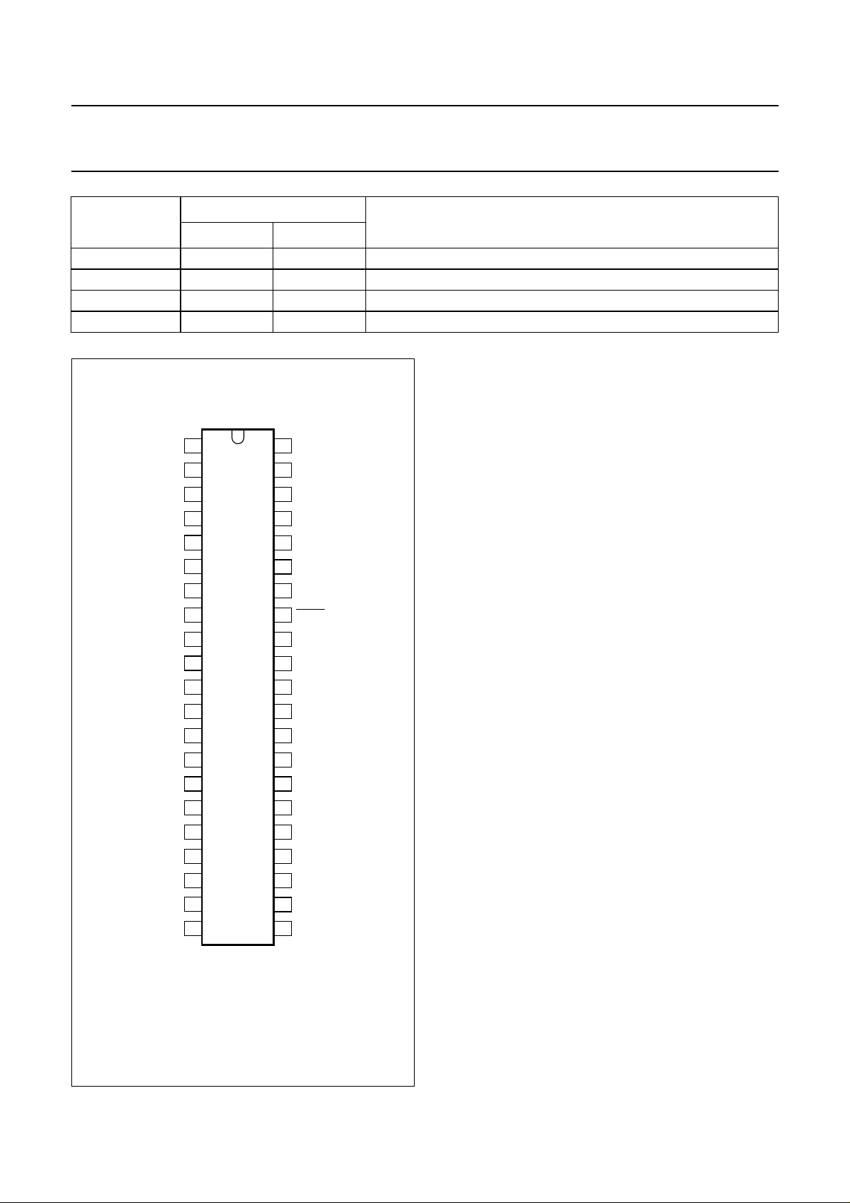
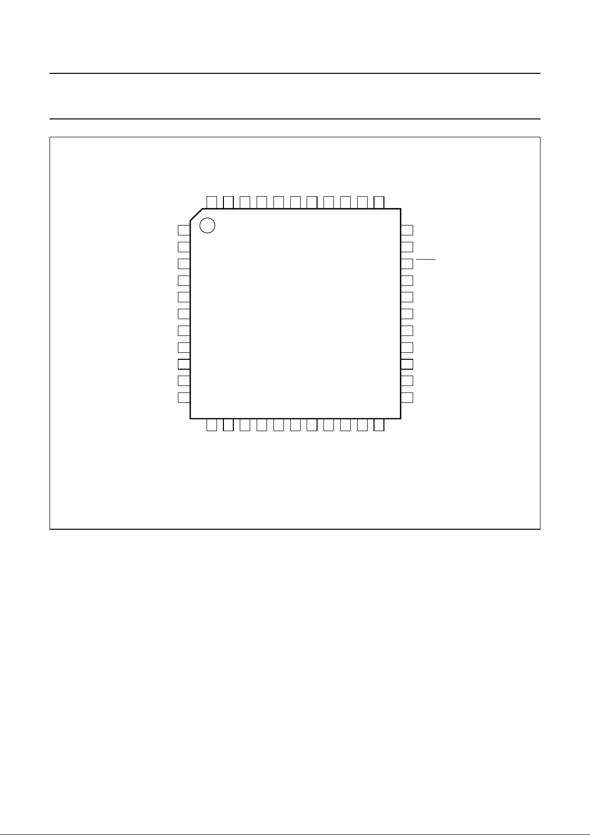
Where pin numbers are mentioned in this data sheet we
refer to the TEA1069N, unless otherwise indicated.
Speech part
The speech/transmission part performs all speech and line
interface functions required in electronic sets. It operates
at line voltages down to 1.6 V DC to facilitate the use of
more telephones connected in parallel.
Dialler part
The dialler part offers a 32-digit Last Number Redial (LNR)
and 13 memories. Hands-free control is included allowing
the TEA1069 and TEA1069A to be used not only in basic
telephones, but also in feature phones offering hands-free
dialling via the TEA1083 call-progress monitor IC and/or
full hands-free operation via the TEA1093 hands-free IC.
The hold function allows the user to suspend the
conversation and resume the call either on the same
phone or on a parallel phone. Additionally through the
music-on-hold function a melody is transmitted while the
set is put on hold. The keytones provide in a buzzer an
audible feedback of a valid key pressed.
1998 Jan 08 2
Page 3
Philips Semiconductors Product specification
Versatile speech/dialler/ringer with
TEA1069; TEA1069A
music-on-hold
Ringer part
The ringer part offers a discriminator input which enables the tone output as soon as a valid ring frequency is detected.
It offers a melody based on 3 tones with programmable melody and volume via keyboard.
ORDERING INFORMATION
TYPE
NUMBER
TEA1069N SDIP42 plastic shrink dual in-line package; 42 leads (600 mil) SOT270-1
TEA1069H QFP44 plastic quad flat package; 44 leads (lead length 1.3 mm);
TEA1069AH QFP44 plastic quad flat package; 44 leads (lead length 1.3 mm);
NAME DESCRIPTION VERSION
body 10 × 10 × 1.75 mm
body 10 × 10 × 1.75 mm
PACKAGE
SOT307-2
SOT307-2
1998 Jan 08 3
Page 4
Philips Semiconductors Product specification
Versatile speech/dialler/ringer with
music-on-hold
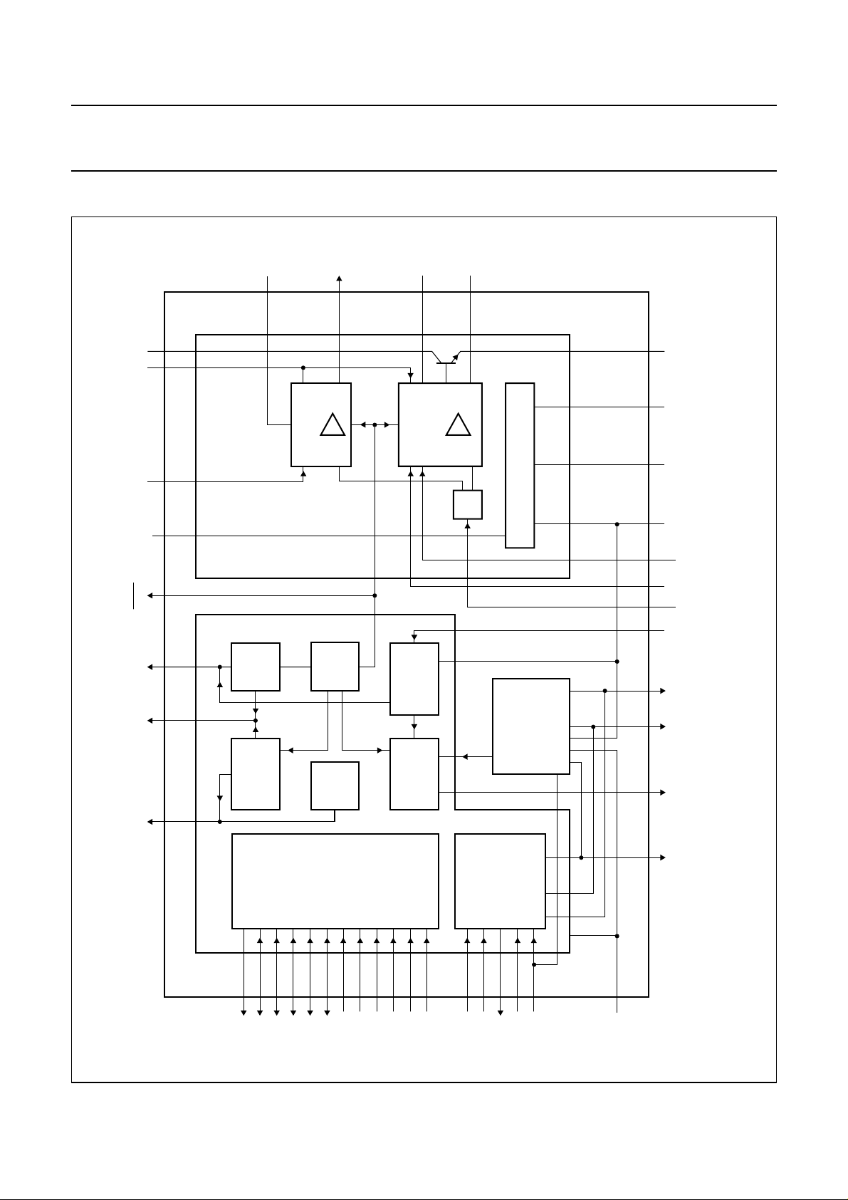
BLOCK DIAGRAM
40
LN
38
AGCIRMUTEMOH/DMODP/FLKT/EARTH
6
36
CC
V
35
27
20
GAR
(40) 2
(36)
(34)
SPEECH
(44)
(32)
(31)
(22)
PULSE
(15)
(39) 1
RECEIVE
SECTION
QR
MUTE
GAS1
(37) 41
SECTION
TRANSMIT
HOLD
LOGIC
GAS2
(38) 42
dB
TEA1069
TEA1069A
SUPPLY
RINGER
TEA1069; TEA1069A
MBH195
(35)
39
SLPE
(43)
5
STAB
(33)
37
REG
(11, 18
and 23)
23
EE
V
(41)
3
MIC−
MIC+
DTMF
HOLD
DETECTOR/
GENERATOR
(42)
(1)
(16)
(17)
(21)
4
7
21
22
26
handbook, full pagewidth
Fig.1 Block diagram.
RECALL
8
(2)
KEY-
TONE
DETECTOR
KEYBOARD
TONE
DIALLER
34 (30)
33 (29)
32 (28)
31 (27)
30 (26)
29 (25)
14 (8)
15 (9)
16 (10)
17 (12)
18 (13)
COL6
COL5
COL4
COL3
ROW5
DIODE
ROW4
ROW3
ROW2
ROW1
COL2
1998 Jan 08 4
GENERATOR
19 (14)
9 (3)
CSI
COL1
10 (4)
XTAL1
TIMING/
CONTROL
11 (5)
12 (6)
XTAL2
13 (7)
CE/FDI
RESET
(19)
(24)
25 (20)
DD
V
24
28
HF TONE VOL1 VOL2
Pin numbers in parenthesis refer to the TEA1069H and TEA1069AH.
Page 5

Philips Semiconductors Product specification
Versatile speech/dialler/ringer with
TEA1069; TEA1069A
music-on-hold
PINNING
SYMBOL
QR 1 39 receiving amplifier output
GAR 2 40 gain adjustment; receiving amplifier
MIC− 3 41 inverting microphone input
MIC+ 4 42 non-inverting microphone input
STAB 5 43 current stabilizer
IR 6 44 receiving amplifier input
DTMF 7 1 dual-tone multi-frequency input
KT/EARTH 8 2 keytone/earth recall output
CSI 9 3 cradle switch input
XTAL1 10 4 oscillator input
XTAL2 11 5 oscillator output
RESET 12 6 reset input
CE/FDI 13 7 chip enable/frequency discrimination input
COL6 14 8 keyboard column input 6
COL5 15 9 keyboard column input 5
COL4 16 10 keyboard column input 4
COL3 17 12 keyboard column input 3
COL2 18 13 keyboard column input 2
COL1 19 14 keyboard column input 1
DP/FL 20 15 dial pulse/flash output
HOLD 21 16 hold control input
VOL2 22 17 volume 2 output
V
EE
TONE 24 19 tone generator output
V
DD
VOL1 26 21 volume 1 output
MOH/DMO 27 22 music on hold/dial mode output
HF 28 24 hands-free control output
ROW1 29 25 keyboard row input/output 1
ROW2 30 26 keyboard row input/output 2
ROW3 31 27 keyboard row input/output 3
ROW4 32 28 keyboard row input/output 4
ROW5 33 29 keyboard row input/output 5
DIODE 34 30 diode option output
MUTE 35 31 mute output, active LOW
V
CC
REG 37 33 (DC) line voltage regulator decoupling
AGC 38 34 automatic gain control input
SOT270-1 SOT307-2
PIN
DESCRIPTION
23 11, 18, 23 negative line terminal
25 20 dialler/ringer part supply voltage
36 32 speech part supply voltage
1998 Jan 08 5
Page 6
Philips Semiconductors Product specification
Versatile speech/dialler/ringer with
TEA1069; TEA1069A
music-on-hold
SYMBOL
SOT270-1 SOT307-2
SLPE 39 35 slope (DC resistance) adjustment
LN 40 36 positive line terminal
GAS1 41 37 gain adjustment; transmitting amplifier
GAS2 42 38 gain adjustment; transmitting amplifier
handbook, halfpage
QR
GAR
MIC−
MIC+
STAB
DTMF
KT/EARTH
CSI
XTAL1
XTAL2
RESET
CE/FDI
COL6
COL5
COL4
COL3
COL2
COL1
DP/FL
HOLD
IR
1
2
3
4
5
6
7
8
9
10
11
TEA1069N
12
13
14
15
16
17
18
19
20
PIN
MBH196
42
GAS2
41
GAS1
40
LN
39
SLPE
38
AGC
37
REG
V
36
35
MUTE
DIODE
34
33
ROW5
ROW4
32
31
ROW3
ROW2
30
29
ROW1
HF
28
27
MOH/DMO
VOL1
26
V
25
TONE
24
V
23
2221
VOL2
DESCRIPTION
CC
DD
EE
Fig.2 Pin configuration (SOT270-1).
1998 Jan 08 6
Page 7
Philips Semiconductors Product specification
Versatile speech/dialler/ringer with
music-on-hold
IR
STAB
handbook, full pagewidth
DTMF
KT/EARTH
CSI
XTAL1
XTAL2
RESET
CE/FDI
COL6
COL5
COL4
V
EE
44
1
2
3
4
5
6
7
8
9
10
11
MIC+
43
42
MIC−
GARQRGAS2
41
40
TEA1069H
TEA1069AH
TEA1069; TEA1069A
GAS1LNSLPE
39
38
37
36
AGC
35
34
33
REG
V
32
CC
MUTE
31
DIODE
30
29
ROW5
ROW4
28
ROW3
27
ROW2
26
ROW1
25
HF
24
V
23
EE
12
13
14
15
COL3
COL2
COL1
DP/FL
Fig.3 Pin configuration (SOT307-2).
FUNCTIONAL DESCRIPTION
Speech part
For numbering of components refer to Figs 28 and 29.
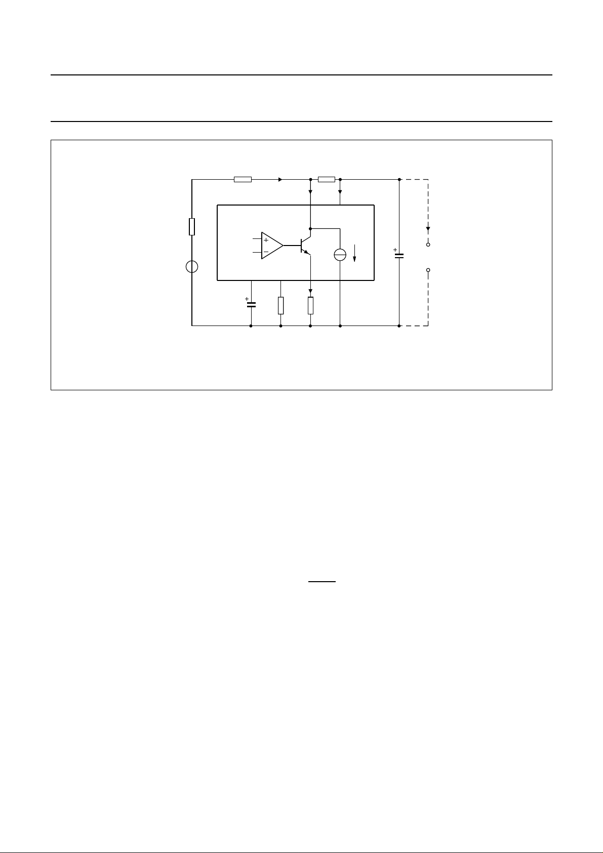
SUPPLIES VCC, LN, SLPE, REG AND STAB
Power for the IC and its peripheral circuits is usually
obtained from the telephone line (see Fig.4).
The circuit creates a stabilized voltage (V
= 3.7 V)
ref
between LN and SLPE. This reference voltage is
temperature compensated and can be adjusted by means
of an external resistor RVA. It can be increased by
connecting an RVA resistor (R60) between REG and SLPE
or decreased by connecting an RVA resistor (R61)
between REG and LN. This internal voltage reference is
decoupled by capacitor C3 between REG and VEE.
16
17
18
19
20
21
22
MBH784
HOLD
VOL2
EE
V
TONE
DD
V
VOL1
MOH/DMO
This decoupling capacitor realises the set impedance
conversion from its DC value to its AC value in the audio
frequency range.
The internal transmission part of the circuitry (including the
earpiece amplifier) is supplied from V
. This voltage
CC
supply is derived from the LN voltage via a dropping
resistor (R1) and must be decoupled by a capacitor (C1)
between VCC and VEE. This supply point may also be used
to supply the dialler/ringer (VDD) part or external circuit e.g.
electret microphone.
The DC current flowing into the set is determined by the
exchange supply voltage V
resistance R
line R
. When the line current (I
line
and the DC resistance of the telephone
exch
, the feeding bridge
exch
) is more than 0.5 mA
line
greater than the sum of the IC supply current (ICC) and the
current drawn by the peripheral circuitry connected to V
(Ip), the excess current is shunted to SLPE via LN.
CC
1998 Jan 08 7
Page 8
Philips Semiconductors Product specification
Versatile speech/dialler/ringer with
music-on-hold
handbook, full pagewidth
V
R
exch
exch
R
line
I
TEA1069
TEA1069A
DC
AC
Fig.4 Supply arrangement.
I
line
+ 0.5 mA
SLPE
LN
SLPESTABREG
I
SLPE
C3 R5 R9
R1
V
I
CC
CC
0.5 mA
V
EE
TEA1069; TEA1069A
I
p
peripheral
C1
circuits
MBH197
Thus, the regulated voltage on the line terminal (VLN) can
be calculated as:
V
I
V
V
LN
SLPEIlineICCIp
ref
refISLPE
–=
is the internally generated temperature compensated
R9×+=
, where
0.5 103–A×++
reference voltage of 3.7 V and R9 is an external resistor
connected between SLPE and V
EE
.
The circuit has an internal current stabilizer operating at a
level determined by resistor R5 connected between STAB
and V
EE
.
In normal use the value of R5 would be 3.6 kΩ and the
value of R9 would be 20 Ω.
Changing the value of R5 or R9 will affect microphone
gain, DTMF gain, gain control characteristics, sidetone
level, maximum output swing on LN and the DC
characteristics (especially at low line current).
At line currents below 9 mA the internal reference voltage
is automatically adjusted to a lower value (typically 1.6 V
at 1 mA). This means that more sets can be operated in
parallel with DC line voltages (excluding the polarity guard)
down to an absolute minimum voltage of 1.6 V. At line
currents below 9 mA the circuit has limited sending and
receiving levels.
Under normal conditions, when I
>> ICC+ 0.5 mA + Ip,
SLPE
the static behaviour of the circuit is that of a 3.7 V regulator
diode (V
) with an internal resistance equal to that of R9.
ref
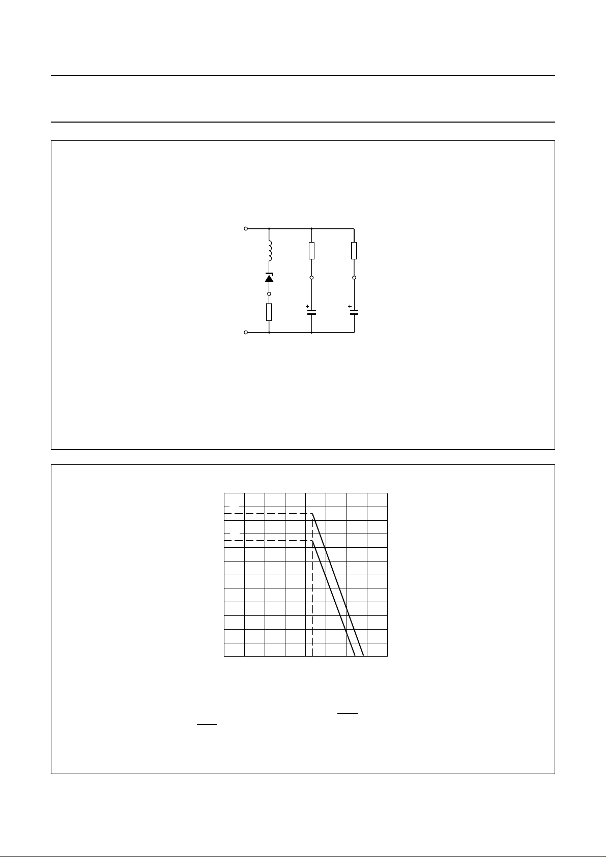
In the audio frequency range the dynamic impedance is
largely determined by R1. Figure 5 shows the equivalent
impedance of the circuit.
Current (Ip) available from VCC for the dialler part and
peripheral circuits depends on the external components
used. Figure 6 shows this current for VCC> 2.2 V. When
MUTE is HIGH i.e. when the receiving amplifier (supplied
from VCC) is driven, the available current is further
reduced. Current availability can be increased by
connecting the supply IC TEA1081 in parallel with R1, or
by increasing the DC line voltage by means of an external
resistor (RVA= R60) connected between REG and SLPE.
1998 Jan 08 8
Page 9
Philips Semiconductors Product specification
Versatile speech/dialler/ringer with
music-on-hold
handbook, halfpage
LN
SLPE
V
EE
L
eq
V
R9
20 Ω
ref
R
REG
p
C3
4.7 µF C1100 µF
R1
V
CC
MGD489
TEA1069; TEA1069A
Leq=C3×R9 × Rp.
Rp= 16.2 kΩ.
Fig.5 Equivalent impedance circuit.
2.4
handbook, halfpage
(1)
I
p
(mA)
(2)
1.6
0.8
0
012 4
3
MSA504
VCC(V)
VCC> 2.2 V; I
(1) Ip= 2.1 mA. The curve is valid when the receiving amplifier is not driven or when MUTE = LOW.
(2) Ip= 1.7 mA. The curve is valid when MUTE = HIGH and the receiving amplifier is driven; V
= 15 mA at VLN= 4 V; R1 = 620 Ω; R9 = 20 Ω.
line
Fig.6 Typical current IP available from VCC for peripheral circuitry.
1998 Jan 08 9
= 150 mV, RL= 150 Ω.
o(rms)
Page 10
Philips Semiconductors Product specification
Versatile speech/dialler/ringer with
TEA1069; TEA1069A
music-on-hold
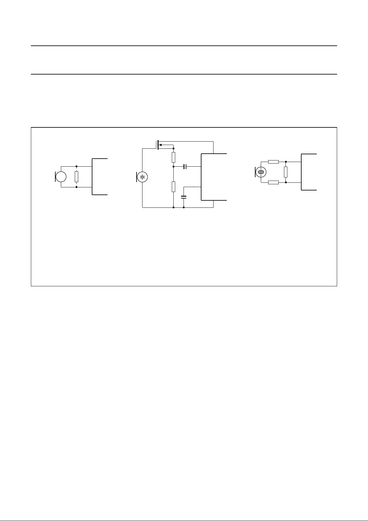
MICROPHONE INPUTS MIC+ AND MIC− AND GAIN PINS GAS1 AND GAS2
The circuit has symmetrical microphone inputs. Its input impedance is 64 kΩ (2 × 32 kΩ) and its voltage gain is typically
52 dB (when R7 = 68 kΩ). Dynamic, magnetic, piezoelectric or electret (with built-in FET source followers) microphones
can be used. Microphone arrangements are illustrated in Fig.7.
handbook, full pagewidth
36 (32)
V
4 (42)
MIC+
(1)
3 (41)
MIC−
a. Magnetic or dynamic
microphone.
3 (41)
MIC−
4 (42)
MIC+
b. Electret microphone.
CC
V
EE
23 (18)
c. Piezoelectric microphone.
4 (42)
3 (41)
MIC+
MIC−
MBH198
Pin numbers in parenthesis refer to the TEA1069H and TEA1069AH.
(1) Resistor may be connected to reduce the terminating impedance.
Fig.7 Alternative microphone arrangements.
The gain of the microphone amplifier can be adjusted
between 44 dB and 52 dB to suit the sensitivity of the
transducer in use. The gain is proportional to the value of
R7 which is connected between GAS1 and GAS2. Stability
is ensured by two external capacitors, C6 connected
between GAS1 and SLPE and C17 connected between
GAS1 and VEE. The value of C6 is 100 pF but this may be
increased to obtain a first-order low-pass filter. The value
of C17 is 10 times the value of C6. The cut-off frequency
corresponds to the time constant R7 × C6.
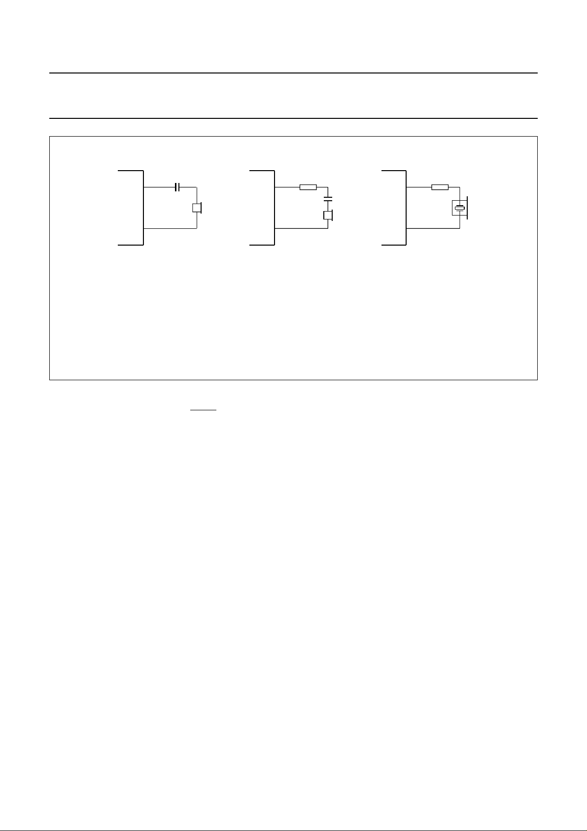
ECEIVING AMPLIFIER IR, QR AND GAR
R
The receiving amplifier has one input (IR) and one output
(QR). Earpiece arrangements are illustrated in Fig.8.
The IR to QR gain is typically 31 dB (when R4 = 100 kΩ).
It can be adjusted between 20 and 31 dB to match the
sensitivity of the transducer in use.
The gain is set with the value of R4 which is connected
between GAR and QR. The overall receive gain, between
LN and QR, is calculated by subtracting the anti-sidetone
network attenuation (32 dB) from the amplifier gain.
Two external capacitors, C4 and C7, ensure stability. C4 is
normally 100 pF and C7 is 10 times the value of C4.
The value of C4 may be increased to obtain a first-order
low-pass filter. The cut-off frequency will depend on the
time constant R4 × C4.
The output voltage of the receiving amplifier is specified for
continuous-wave drive. The maximum output voltage will
be higher under speech conditions where the peak to RMS
ratio is higher.
1998 Jan 08 10
Page 11
Philips Semiconductors Product specification
k
Versatile speech/dialler/ringer with
music-on-hold
, full pagewidth
1 (39)
QR
23 (18)
V
EE
a. Dynamic earpiece. b. Magnetic earpiece. c. Piezoelectric earpiece.
Pin numbers in parenthesis refer to the TEA1069H and TEA1069AH.
(1) Resistor may be connected to prevent distortion (inductive load).
(2) Resistor is required to increase the phase margin (capacitive load).
Fig.8 Alternative receiver arrangements.
(1) (2)
1 (39)
QR QR
23 (18)
V
EE
TEA1069; TEA1069A
1 (39)
23 (18)
V
EE
MBH199
DUAL TONE MULTI-FREQUENCY INPUT DTMF
When the DTMF input is enabled (MUTE is LOW) dialling
tones may be sent on to the line. The voltage gain from
DTMF to LN is typically 25.5 dB (when R7 = 68 kΩ) and
varies with R7 in the same way as the microphone gain.
The tones can be heard in the earpiece at a low level
(confidence tone).
microphone amplifier and the receiving amplifier in
accordance with the DC line current.
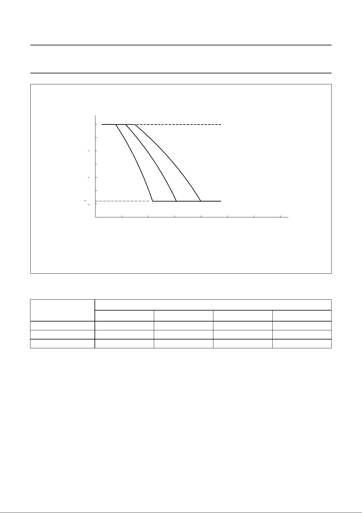
The control range is 5.8 dB which corresponds to a line
length of 5 km for a 0.5 mm diameter twisted-pair copper
cable with a DC resistance of 176 Ω/km and average
attenuation of 1.2 dB/km. Resistor R6 should be chosen in
accordance with the exchange supply voltage and its
feeding bridge resistance (see Fig.9 and Table 1).
A
UTOMATIC GAIN CONTROL INPUT AGC
Automatic line loss compensation is achieved by
connecting a resistor (R6) between AGC and VEE.
The automatic gain control varies the gain of the
The ratio of start and stop currents of the AGC curve is
independent of the value of R6. If no automatic line-loss
compensation is required the AGC pin may be left
open-circuit. The amplifiers, in this condition, will give their
maximum specified gain.
1998 Jan 08 11
Page 12
Philips Semiconductors Product specification
Versatile speech/dialler/ringer with
music-on-hold
handbook, full pagewidth
0
∆G
v
(dB)
2
5.8
4
6
78.7 kΩ
R6 = ∞
110 kΩ 140 kΩ
TEA1069; TEA1069A
MGD490
I (mA)
140120100806040200
line
Fig.9 Variation of gain as function of line current with R6 as parameter.
Table 1 Values of resistor R6 for optimum line-loss compensation at various values of exchange supply voltage
(V
) and exchange feeding bridge resistance (R
exch
); R9 = 20 Ω
exch
R6 (kΩ)
V
(V)
exch
R
= 400 Ω R
exch
= 600 Ω R
exch
= 800 Ω R
exch
exch
= 1000 Ω
36 100 78.7 −−
48 140 110 93.1 82
60 −−120 102
1998 Jan 08 12
Page 13
Philips Semiconductors Product specification
Versatile speech/dialler/ringer with
music-on-hold
SIDETONE SUPPRESSION
Suppression of the transmitted signal in the earpiece is
obtained by the anti-sidetone network comprising R1//Z
R2, R3, R8, R9 and Z
(see Fig.10). The maximum
bal
compensation is obtained when the following conditions
are fulfilled:
R9 R2× R1 R3 R8+()×=
kR3
Z
bal
R8 R9+()
×=
----------------------------R2 R9×()
kZ
×=
line
The scale factor k is chosen to meet the compatibility with
a standard capacitor from the E6 or E12 series for Z
In practice, Z
length. Therefore, the value chosen for Z
varies considerably with the line type and
line
should be for
bal
an average line length thus giving optimum setting for
short or long lines.
Example: the balance impedance Z
at which the
bal
optimum suppression is present can be calculated as
line
line
(1)
(2)
(3)
.
TEA1069; TEA1069A
follows:
suppose Z
5 km line of 0.5 mm diameter, copper, twisted-pair cable
,
matched to 600 Ω (176 Ω/km; 38 nF/km).
When k = 0.64 then R8 = 390 Ω;
Z
= 130 Ω + (820 Ω//220 nF).
bal
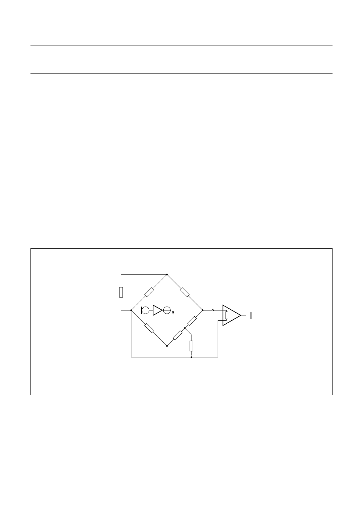
The anti-sidetone network for the TEA1069 and
TEA1069A shown in Fig.10 attenuates the signal received
from the line by 32 dB before it enters the receiving
amplifier.
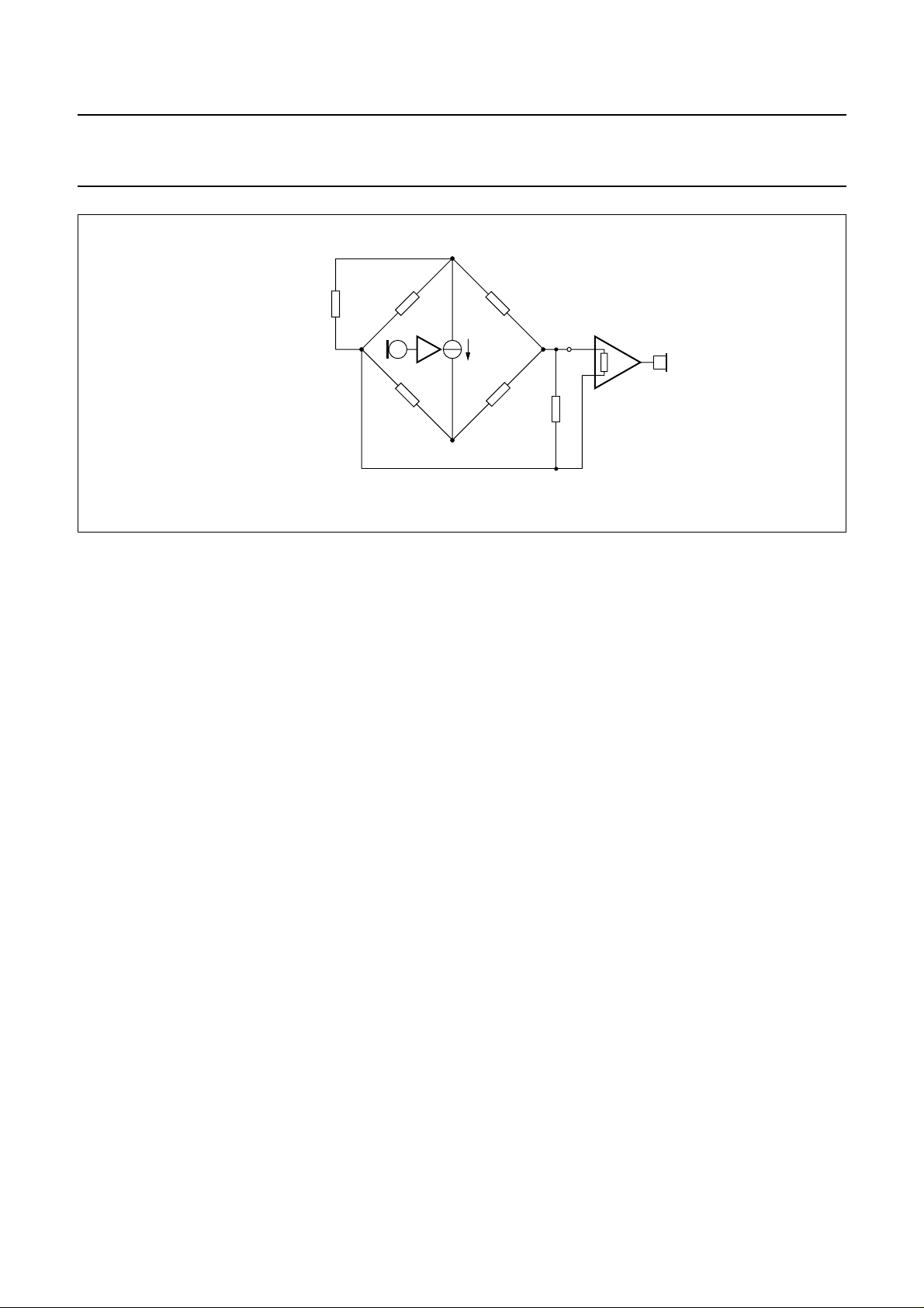
The attenuation is almost constant over the whole
audio-frequency range. Figure 11 shows a conventional
Wheatstone bridge anti-sidetone circuit that can be used
as an alternative. Both bridge types can be used with
either resistive or complex set impedances. More
information on the balancing of anti-sidetone bridges can
be found in our publication
Wired telecom systems, IC03b”
9397 750 00811.
= 210 Ω + (1265 Ω//140 nF) representing a
line
“Applications Handbook for
, order number
handbook, full pagewidth
LN
Z
line
V
EE
R1 R2
i
m
R9
R8
SLPE
R3
IR
R
t
Z
bal
MSA500 - 1
Fig.10 Equivalent circuit of TEA1069 and TEA1069A anti-sidetone bridge.
1998 Jan 08 13
Page 14
Philips Semiconductors Product specification
Versatile speech/dialler/ringer with
music-on-hold
handbook, full pagewidth
Z
line
V
EE
Fig.11 Equivalent circuit of an anti-sidetone network in a Wheatstone bridge configuration.
Dialler and ringer part
UPPLY VOLTAGE: PINS VDDAND V
S
EE
The power supply must be maintained for data storage.
The RAM retention voltage (standby supply voltage) may
drop down to 1.0 V. Applying a large capacitor across the
supply terminals can retain the memory if power
connections are broken. The minimum operation voltage is
2.5 V. The internal power-on reset is enabled for a voltage
below this minimum operation voltage.
O
SCILLATOR INPUT/OUTPUT: PINS XTAL1AND XTAL2
Time base for the TEA1069 and TEA1069A is a
crystal-controlled on-chip oscillator which is completed by
connecting a 3.579545 MHz crystal or ceramic resonator
between XTAL1 and XTAL2. The oscillator starts when
VDD reaches the operation voltage level and
CE/FDI = HIGH. The following types of ceramic
resonators are recommended:
• Kyocera PBRC3.58ARPC10 (wired)
• Kyocera KBR3.58MSATRPC10 (SMD)
• Murata CSA3.58MG310VA (wired).
R
ESET INPUT: PIN RESET
Pin RESET is an input to the internal reset circuit. When
RESET = HIGH, it can be used to initialize the TEA1069
and TEA1069A which is normally done by the CE/FDI
input. The on-chip power-on reset generates a reset pulse
if VDD drops below 2.5 V. In this event a proper start-up
R1
R9
TEA1069; TEA1069A
LN
Z
bal
i
m
R8
SLPE
occurs after the supply voltage rises above the minimum
operation voltage level again.
During and directly after reset pins 14 to 19, 21, 29 to 32,
34 and 35 are set HIGH; pins 8, 20, 22, 26 to 28 and 33
are set to LOW.
The RESET pin can be connected to V
resistor of 100 kΩ to 1 MΩ, which will save leakage
current. A capacitor connected to VDD can be used to
extend the reset time, in case a longer reset is desirable.
To prevent the dialler from reacting on voltage
disturbances on the telephone line a time-out is active.
The dialler returns to standby state if the voltage on the line
has disappeared for more than this reset-delay time (trd).
C
HIP ENABLE/FREQUENCY DISCRIMINATOR INPUT:
PIN CE/FDI
This active HIGH input is used to initialize part of the
system, to select the on-line, standby, or ringer mode and
to detect line power breaks. To keep the TEA1069 and
TEA1069A in the on-line mode, CE/FDI has to be HIGH.
In the exchange, several AC signals can be superimposed
on the DC signal, e.g. dialling tone, busy tone,
disturbances (like line power breaks), and the ringer
signal. The ringer signal is evaluated, and checked if its
frequency is within the limits of the frequency interval as
set by the diode option RFS. It is assumed that the ringer
frequency at pin CE/FDI is the double of the frequency
present on the telephone line.
IR
R
t
R
A
MSA501 - 1
, preferably via a
EE
1998 Jan 08 14
Page 15
Philips Semiconductors Product specification
Versatile speech/dialler/ringer with
music-on-hold
handbook, full pagewidth
In case of a valid ringer signal the user is alerted through
a melody at the TONE output, generated by the ringer part
of the TEA1069 and TEA1069A. This melody follows the
cadence of the ringer signal. Both the melody and the
volume can be selected. The melody frequency and
duration are given in Table 2.
Table 2 Ringer melodies
NAME FREQUENCY (Hz) DURATION (ms)
Bell 1 800 + 1066 + 1333 28 + 28 + 28
Bell 2 826 + 925 + 1027 28 + 28 + 28
Bell 3 1037 + 1161 + 1297 28 + 28 + 28
Bell 4 1297 + 1455 + 1621 28 + 28 + 28
C
RADLE SWITCH INPUT: PIN CSI
To distinguish among different operating states after
CE/FDI is activated, input CSI is used. The basic states
are shown in Table 3.
Table 3 TEA1069 and TEA1069A basic states
INPUT CSI INPUT CE/FDI STATE
LOW LOW standby
HIGH LOW not applicable
LOW HIGH ringer
HIGH HIGH on-line
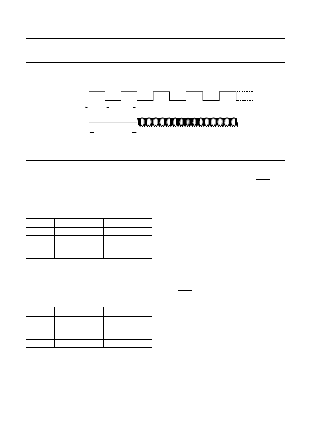
CE/FDI
TONE
sync
time
ringer response delay
(<1.5 frequency cycle)
sample
time
Fig.12 Ringer frequency detection.
TEA1069; TEA1069A
V
DD
V
EE
MBH200
For the hands-free state refer to Fig.23.
P
ULSE DIALLER: PINS DP/FL, MOH/DMO AND MUTE
The pulse dialling system uses line current interruptions to
signal the digits dialled to the exchange. The number of
line current interruptions corresponds with the digit dialled
except for the digit [0] which is characterized by
10 interruptions. Before each digit there is an inter-digit
pause.
Valid keys are the digits [0] to [9] and [PAUSE].
The pulse dialling mode, the make/break ratio and the
access pause time depend on the diode options: PTS,
M/B, APT and APT2. DP/FL is LOW when VDD is below
power-on reset trip level and when RESET is HIGH.
The MOH/DMO pin (diode GOS = on) is used to reduce
the voltage swing over the a/b terminals during pulse
dialling. Several countries require this feature. The MUTE
pin is an open drain output which requires a pull-up
resistor.MUTE is HIGH when VDD is below power-on reset
trip level and when RESET is HIGH.
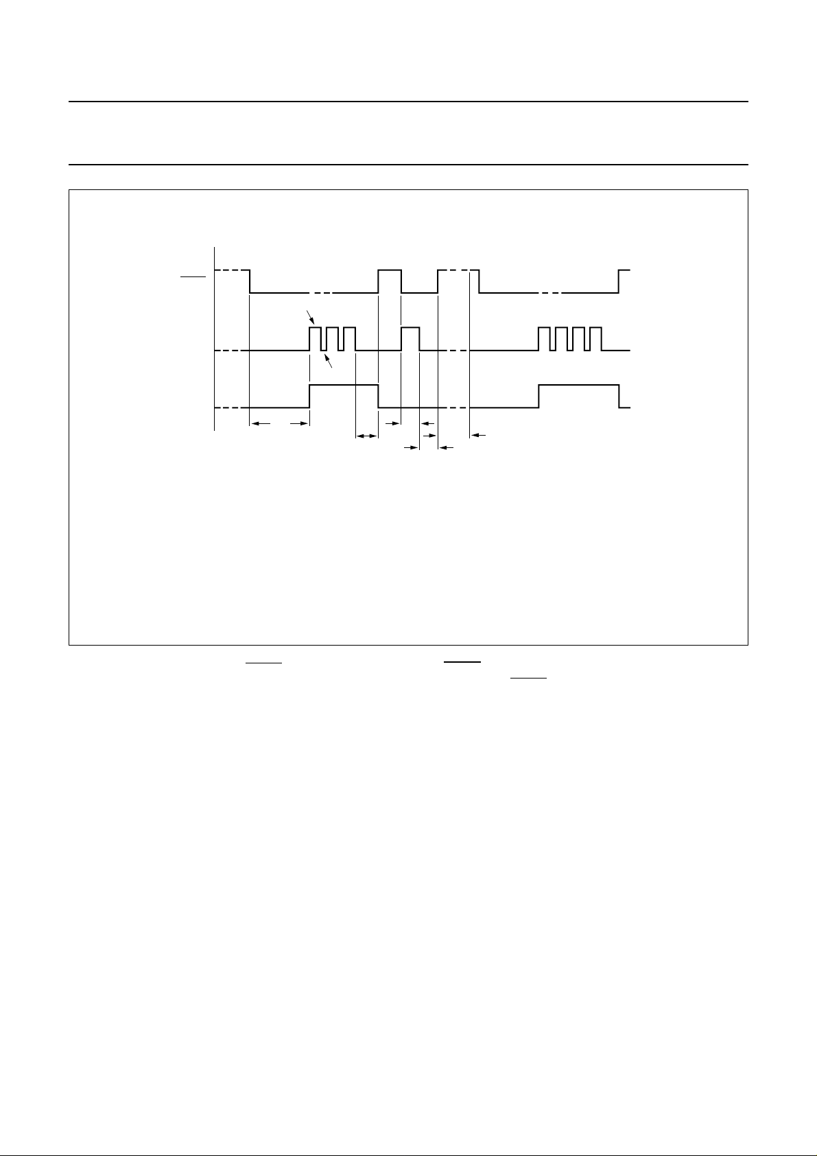
Figure 13 shows the timing diagram in pulse dialling mode
when keys [3], [RECALL] and [4] are pressed.
1998 Jan 08 15
Page 16
Philips Semiconductors Product specification
Versatile speech/dialler/ringer with
music-on-hold
handbook, full pagewidth
tb= break time.
tm= make time.
t
= interdigit pause time.
idp
trc= recall time.
t
= hold-over time.
holdover
t
= interflash hold-over time (only for TEA1069A).
interflash
KEYS
MUTE
DP/FL
MOH/DMO
[3]
t
b
t
m
t
idp
tm + t
[recall] [4]
t
rc
holdover
t
holdover
t
interflash
TEA1069; TEA1069A
MBH201
Fig.13 Timing diagram in pulse dialling mode.
TONE DIALLER: PINS TONE AND MUTE
In this system digits are transmitted as two tones
simultaneously, the so called Dual-Tone Multi-Frequency
(DTMF) system. Tone digits are separated by a pause
time. Valid keys are the digits [0] to [9], [∗], [#] and
[PAUSE].
The DTMF dialling mode, the tone burst/pause times and
the access pause time depend on the diode options: PTS,
TBT, APT and APT2.
MUTE pin is an open drain output which requires a
The
pull-up resistor. MUTE is HIGH when VDD is below
power-on reset trip level and when RESET is HIGH.
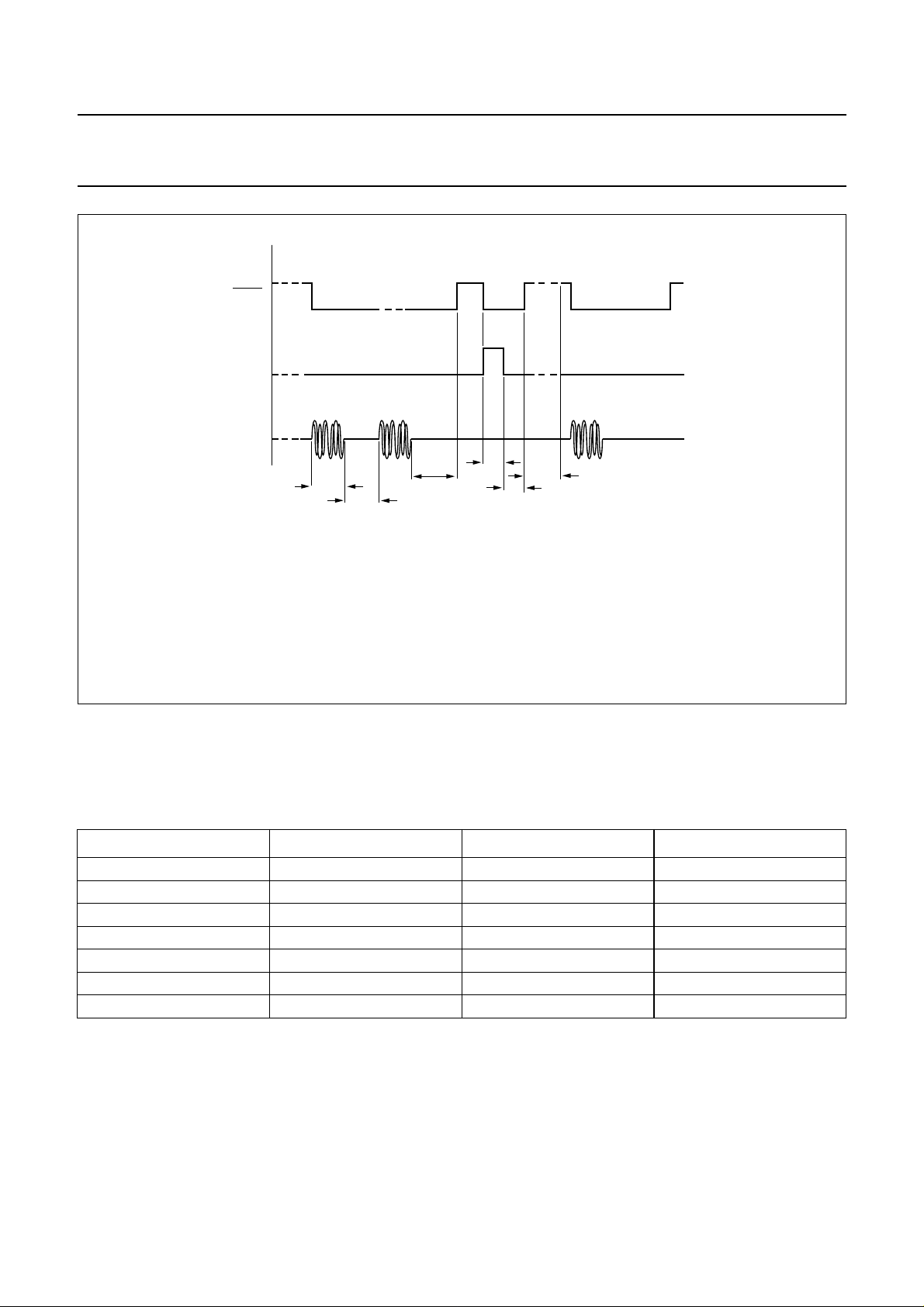
Figure 14 shows the timing diagram in tone dialling mode
when successively keys [3], [3], [RECALL] and [4] are
dialled.
1998 Jan 08 16
Page 17
Philips Semiconductors Product specification
Versatile speech/dialler/ringer with
music-on-hold
handbook, full pagewidth
tt= burst time.
tp= pause time.
t
= hold-over time.
holdover
trc= recall time.
t
= interflash hold-over time (only for TEA1069A).
interflash
KEYS
MUTE
DP/FL
TONE
[3] [3]
t
t
t
p
tp + t
[recall] [4]
t
rc
t
holdover
holdover
TEA1069; TEA1069A
t
interflash
MBH202
Note: in case of manual dialling only the minimum tone burst and pause time values depend on the chosen diode option, the maximum tone burst/pause
times are equal to the real key press/release time.
Fig.14 Timing diagram in tone dialling mode.
The DC-level at the TONE output measures1⁄2VDD and the impedance is typically 100 Ω. DTMF frequencies are
composed by transmitting 2 tones simultaneously at pin TONE. The frequency tolerance for the tones at output TONE
is shown in Table 4.
Table 4 DTMF frequency tolerances
DTMF FREQUENCY FREQUENCY AT TONE DEVIATION (%) DEVIATION (Hz)
697 697.90 +0.13 +0.90
770 770.46 +0.06 +0.46
852 850.45 −0.18 −1.55
941 943.23 +0.24 +2.23
1209 1206.45 −0.21 −2.55
1336 1341.66 +0.42 +5.66
1477 1482.21 +0.35 +5.21
1998 Jan 08 17
Page 18
Philips Semiconductors Product specification
Versatile speech/dialler/ringer with
TEA1069; TEA1069A
music-on-hold
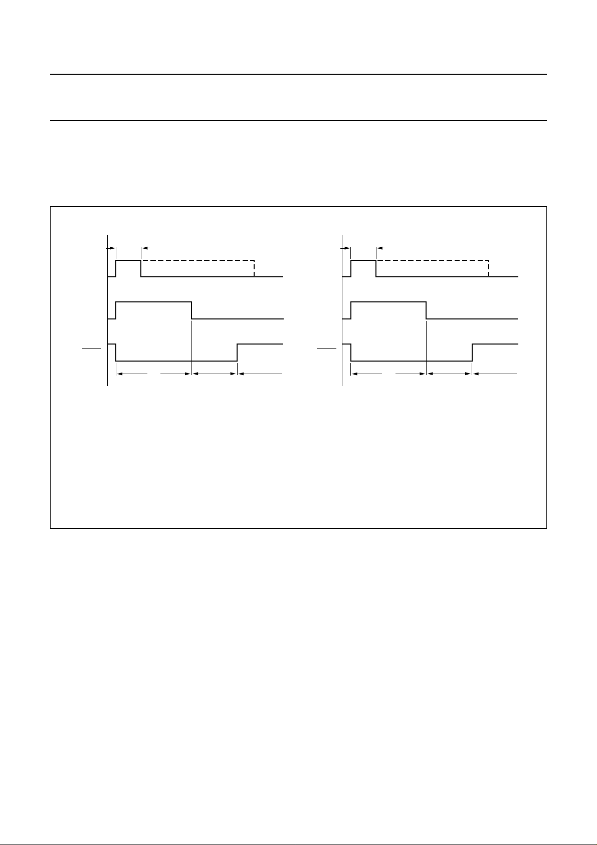
REGISTER RECALL: PINS DP/FL AND KT/EARTH
The RECALL function results in a calibrated pulse which drives the electronic line current interrupter via pin DP/FL or
KT/EARTH. Flash or earth selection and various flash interruption times depend on the diode options: FES A and FES B
(diode GOS = on; see Fig.15).
handbook, full pagewidth
recall
KEY
DP/FL
MUTE
t
kd
recall
KEY
KT/EARTH
MUTE
t
t
rc
holdover
t
interflash
t
kd
t
t
ea
holdover
t
idp
MBH203
a. Recall using flash; trc= recall time using flash. b. Recall using earth; tea= recall time using earth.
tkd= key pressed time (depends on user).
t
= hold-over time.
holdover
t
= interdigit pause time.
idp
t
= interflash hold-over time (only for TEA1069A).
interflash
Fig.15 Recall mode timing diagram.
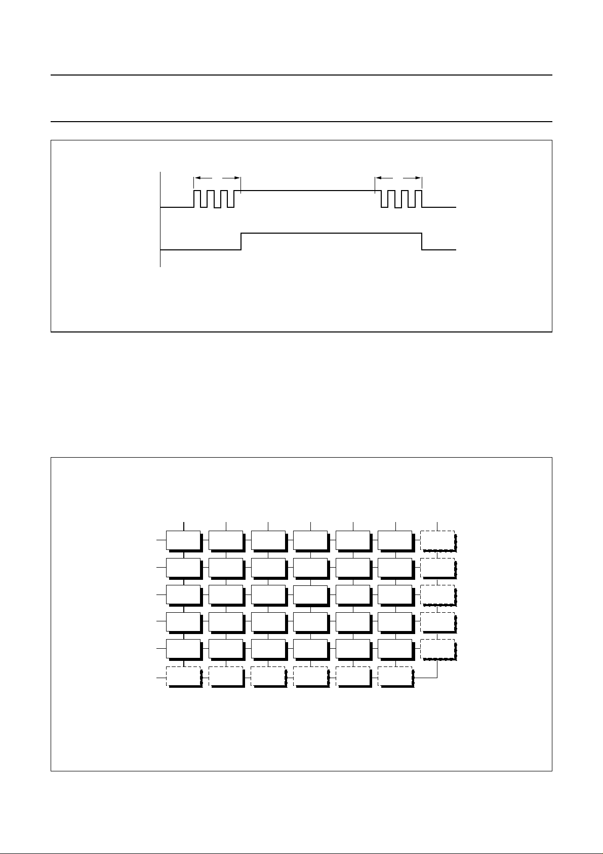
KEYBOARD: PINS ROW1 TO ROW5 AND COL1 TO COL6
The sense columns inputs and scanning rows outputs are
directly connected to a single contact keyboard matrix.
A second key entry will be valid after having released the
first button and after having pressed the second button.
Simultaneously pressing 2 buttons will disable the first
entered key. A key entry becomes valid when the
debounce time td has elapsed.
The column and row pins (except ROW5) are HIGH when
V
is below power-on reset trip level and when RESET is
DD
HIGH.
ROW5 is an open-drain input/output; this configuration is
used to avoid current flowing in the on-line or standby
state. A pull-up resistor should be connected to ROW5.
ROW5 is LOW when VDD is below power-on reset trip level
and when RESET is HIGH.
1998 Jan 08 18
Page 19
Philips Semiconductors Product specification
Versatile speech/dialler/ringer with
music-on-hold
handbook, full pagewidth
key entry
key valid
td= debounce time.
Keyboard layout
The TEA1069 and TEA1069A support three different keyboard layouts:
• With 10 direct accessible repertory numbers
• With 10 indirect accessible repertory numbers
• With 3 direct accessible repertory numbers and 10 indirect numbers.
t
d
Fig.16 Timing diagram debouncing.
TEA1069; TEA1069A
t
d
MBH204
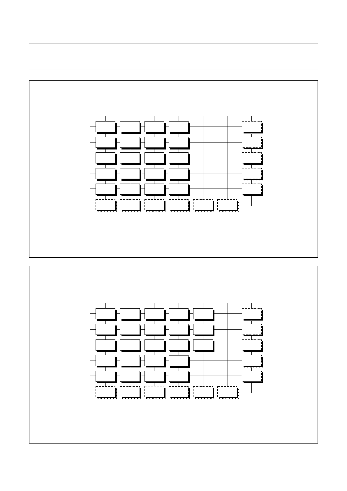
For layouts see Figs 17 to 19; the keyboard layout can be selected by diode option KBS.
handbook, full pagewidth
ROW1
ROW2
ROW3
ROW4
ROW5
DIODE
COL1
1
4
7
/T
*
RECALL
M/B
COL2
2
5
8
0
PAUSE/
LNR
RFS
COL3
3
6
9
#
HOLD/
MUTE
COL4
STORE
MRC
VOL+
VOL−
HOOK
HMSAPT2
COL5
M1
M3
M5
M7
M9
APT
COL6 DIODE
M2
M4
M6
M8
M10
PTS
FES A
FES B
TBT
GOS
KBS
MBH205
Fig.17 Keyboard and diodes with 10 direct accessible repertory numbers.
1998 Jan 08 19
Page 20
Philips Semiconductors Product specification
Versatile speech/dialler/ringer with
music-on-hold
handbook, full pagewidth
ROW1
ROW2
ROW3
ROW4
ROW5
DIODE
COL1
1
4
7
/T
*
RECALL
M/B
COL2
2
5
8
0
PAUSE/
LNR
RFS
COL3
3
6
9
#
HOLD/
MUTE
COL4
STORE
MRC
VOL+
VOL−
HOOK
HMSAPT2
COL5
APT
TEA1069; TEA1069A
COL6 DIODE
FES A
FES B
TBT
GOS
KBS
PTS
MBH206
handbook, full pagewidth
Fig.18 Keyboard and diodes with 10 indirect accessible repertory numbers.
ROW1
ROW2
ROW3
ROW4
ROW5
DIODE
COL1
1
4
7
/T
*
RECALL
M/B
COL2
2
5
8
0
PAUSE/
LNR
RFS
COL3
3
6
9
#
HOLD/
MUTE
APT2
COL4
STORE
MRC
VOL+
VOL−
HOOK
HMS
COL5
M1
M2
M3
APT
COL6 DIODE
FES A
FES B
TBT
GOS
KBS
PTS
MBH207
Fig.19 Keyboard and diodes with 3 direct and 10 indirect accessible repertory numbers.
1998 Jan 08 20
Page 21
Philips Semiconductors Product specification
Versatile speech/dialler/ringer with
TEA1069; TEA1069A
music-on-hold
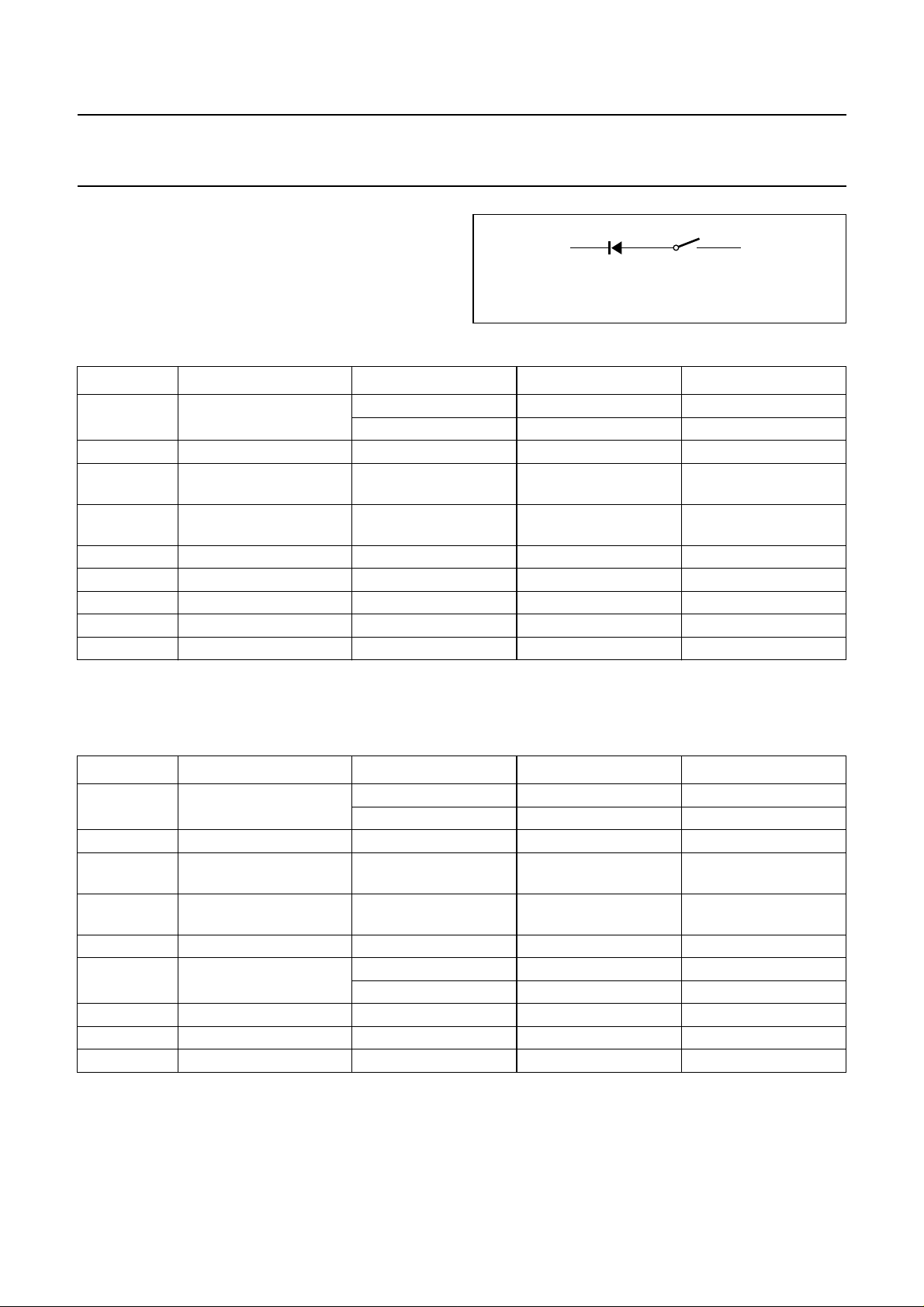
DIODE OPTIONS: PIN DIODE
The DIODE pin is connected to the keyboard matrix as
shown in Fig.20.
The diode options are read after each reset of the dialler.
Table 5 DIODE functions; TEA1069
DIODE FUNCTION CONDITION ON
FES A flash/earth time select FES B = off flash of 270 ms flash of 100 ms
FESB=on earth of 400 ms flash of 600 ms
TBT tone burst/pause time 85/85 ms 100/100 ms
GOS german output select pin 8 = earth;
KBS keyboard select keyboard layout;
PTS pulse/tone selection pulse mode DTMF mode
APT access pause time APT2 = off 4s 2s
HMS hold/mute select hold mode mute mode
RFS ringer frequency select 29to 146 Hz 40 to 120 Hz
M/B make/break ratio 3 : 2 2 : 1
handbook, halfpage
pin 27 = DMO
see Figs 17 and 18
off
on
Fig.20 Diode connection.
(1)
pin 8 = keytone;
pin 27 = MOH
keyboard layout;
see Fig.19
ROW/COLUMNDIODE
OFF
MBH208
(1)
Note
1. on means option diode present; off means option diode not present.
Table 6 DIODE functions; TEA1069A
DIODE FUNCTION CONDITION ON
(1)
OFF
FES A flash/earth time select FES B = off flash of 270 ms flash of 100 ms
FESB=on earth of 400 ms flash of 600 ms
TBT tone burst/pause time 85/85 ms 100/100 ms
GOS german output select pin 8 = earth;
pin 27 = DMO
KBS keyboard select keyboard layout;
see Fig.19
pin 8 = keytone;
pin 27 = MOH
keyboard layout;
see Figs 17 and 18
PTS pulse/tone selection pulse mode DTMF mode
APT access pause time APT2 = off 4s 1s
APT2 = on 3s 2s
HMS hold/mute select hold mode mute mode
RFS ringer frequency select 40to 120 Hz 29 to 146 Hz
M/B make/break ratio 3 : 2 2 : 1
Note
1. on means option diode present; off means option diode not present.
(1)
1998 Jan 08 21
Page 22
Philips Semiconductors Product specification
Versatile speech/dialler/ringer with
music-on-hold
KEY TONE: PIN KT/EARTH
Every time a valid key is pressed a keytone is generated
with a frequency of 606 Hz and a duration of 30 ms. This
function is selected by the diode GOS = off. KT/EARTH is
LOW when VDD is below power-on reset trip level and
when RESET is HIGH.
V
OLUME CONTROL: PINS VOL1 AND VOL2
Both pins can control the volume of the ringer and/or the
hands-free circuit. The state of VOL1/VOL2 is controlled
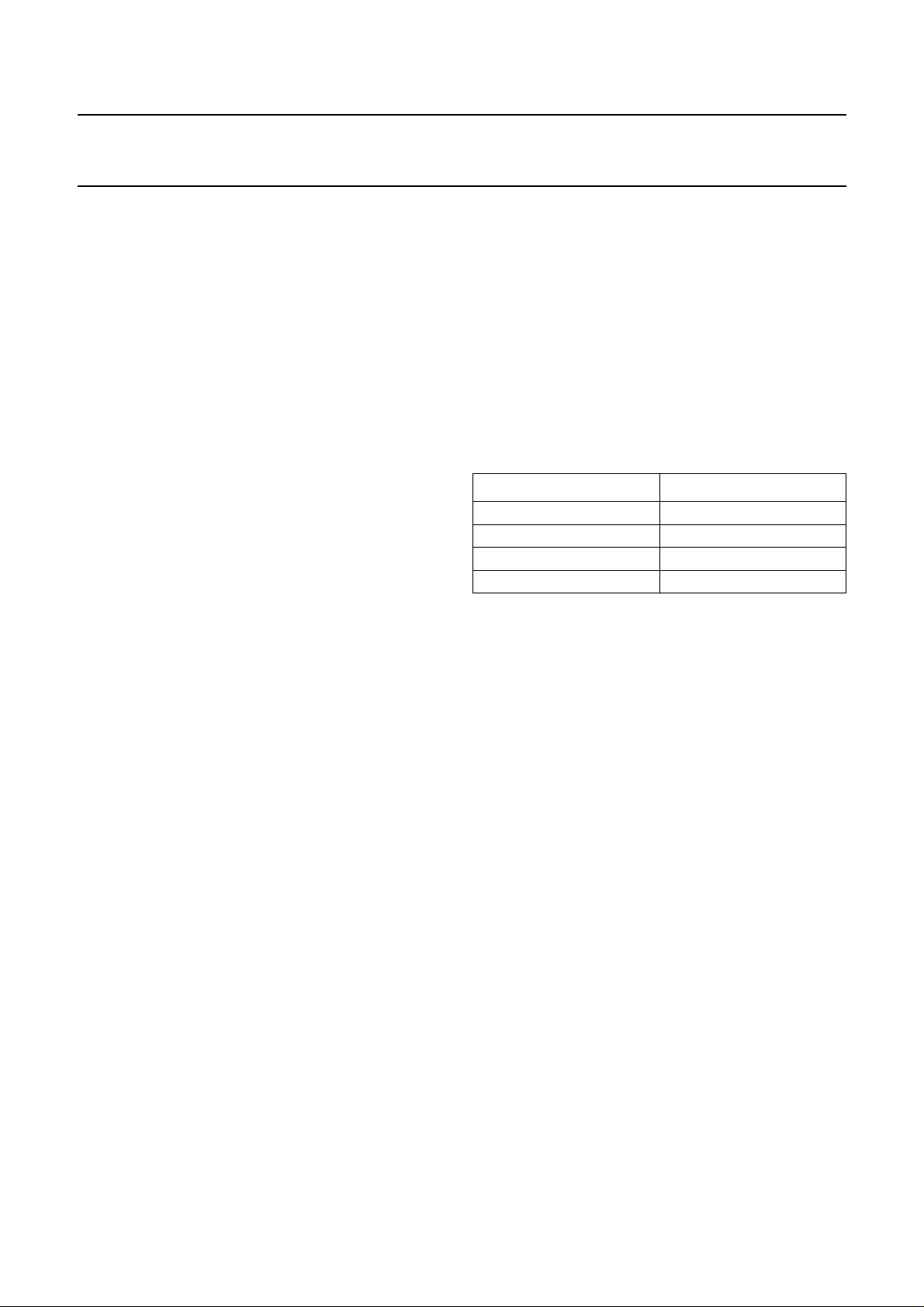
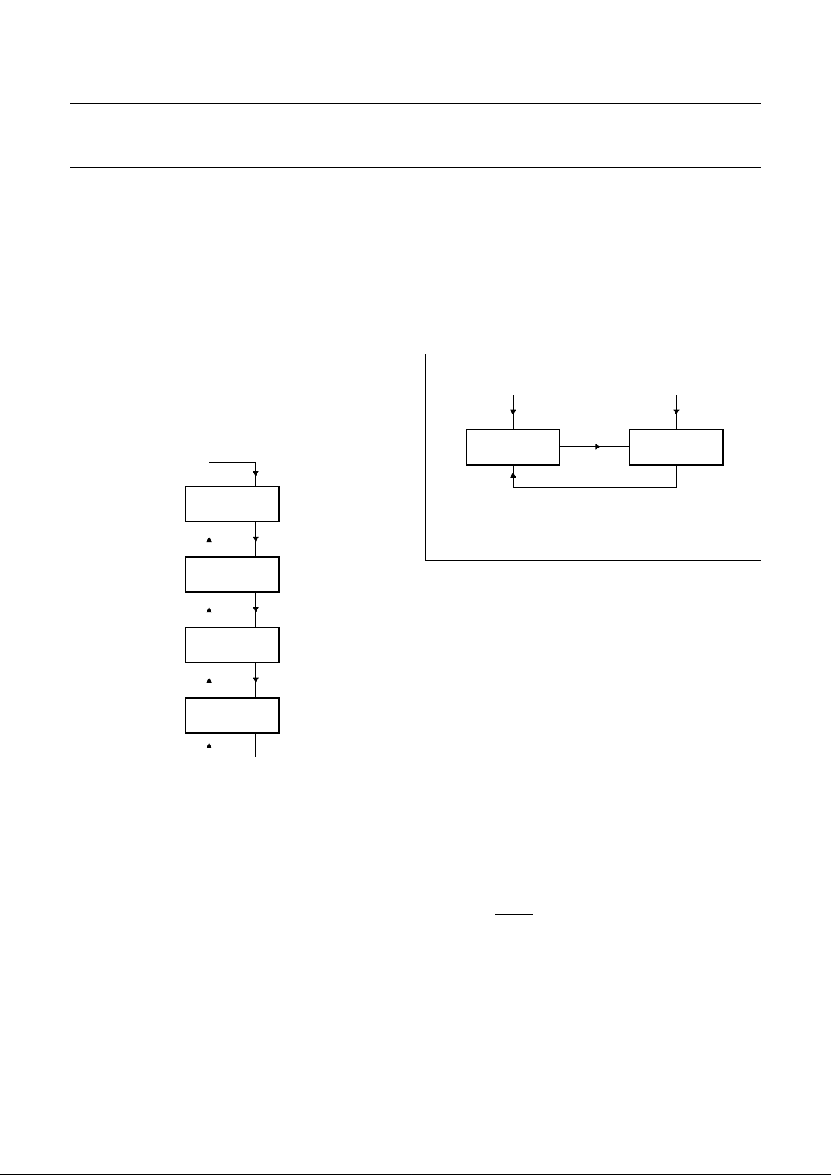
by a state machine as depicted in Fig.24.
VOL1 and VOL2 are push-pull outputs. Both are set LOW
when VDD is below power-on reset trip level and when
RESET is HIGH.
USIC-ON-HOLD: PIN MOH/DMO
M
When the dialler is in the hold state (see Fig.23) a melody
is generated via pin TONE. In this state pin MOH/DMO can
be used via diode GOS = off as an enable signal for the
hardware to indicate that the tone should be switched to
the telephone line.
MOH/DMO is a push-pull output. It is set LOW when V
is below power-on reset trip level and when RESET is
HIGH.
DD
TEA1069; TEA1069A
HANDS-FREE: PIN HF
During the on-line state, the hands-free output pin HF is
used for enabling the hands-free hardware. The pin will
change state depending on specific key-sequences
(see Fig.23).
HF is a push-pull output. It is set LOW when VDD is below
power-on reset trip level and when RESET is HIGH.
MODE: PIN HOLD
HOLD
One way to terminate the hold state (see Fig.23) is a
change in state of the signal at pin HOLD. This input
should reflect the line current. If current is flowing the
signal at pin HOLD should be HIGH, if not it should be
LOW.
This pin is not debounced. The signal applied should be
filtered by the hardware. HOLD is HIGH when VDD is below
power-on reset trip level and when RESET is HIGH.
Key sequences
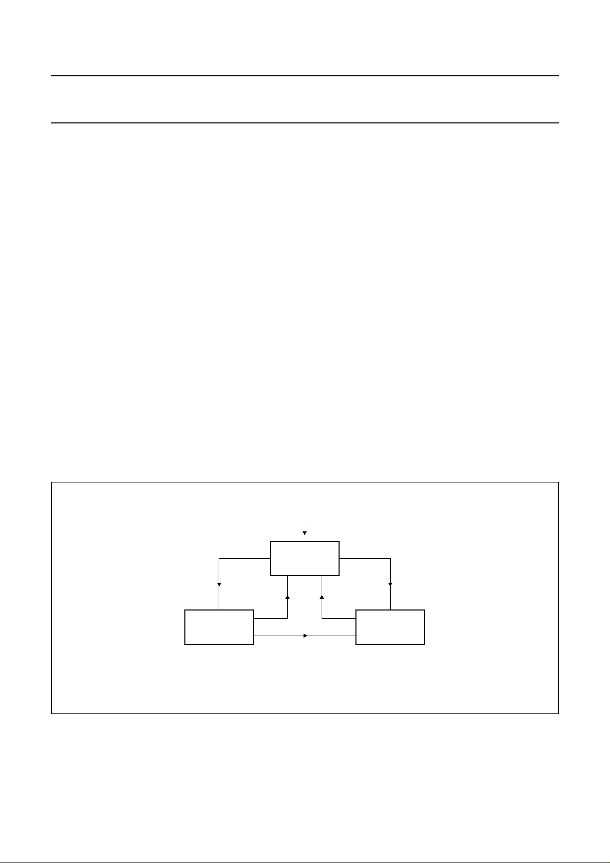
The behaviour of the TEA1069 and TEA1069A can be
modelled as a State Transition Diagram (STD) shown in
Fig.21.
handbook, full pagewidth
ringer signal
ringer invalid
power-on
STANDBY
off-hook/[HOOK]
Fig.21 TEA1069 and TEA1069A dialler/ringer states.
1998 Jan 08 22
off-hook/[HOOK]
on-hook/[HOOK]
ON-LINERINGER
MBH209
Page 23
Philips Semiconductors Product specification
Versatile speech/dialler/ringer with
music-on-hold
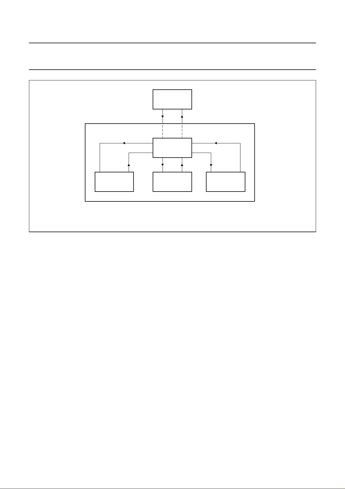
The STD contains the states (rectangles in the figure) and
state transitions (arrows) of the set. The upper arrow in the
figure pointing to the standby state means that the set is
initially in the standby state. When for instance an
incoming call is detected, the set enters the ringer state,
waiting for a reaction of the user. If the user answers the
call on a handset, the set enters the on-line state.
The TEA1069 and TEA1069A have 3 basic states:
• Standby state
• Ringer state
• On-line state.
Each state with its own functional requirements is
described in the following sections.
S
TANDBY STATE
In standby state the TEA1069 and TEA1069A are inactive.
The current drawn is for memory retention and depends on
the loads of the inputs/outputs of the dialler. In this state
output DP/FL is HIGH so that the line is disconnected.
TEA1069; TEA1069A
RINGER STATE
If the set is in standby mode, a ringer signal can be
received from the line. After evaluating the incoming ringer
signal (and ringer signal is valid), the TEA1069 and
TEA1069A start a melody via the TONE output ringer
hardware, and stops this melody if the ringer signal is not
valid any more. After going off-hook, the ringer signal stops
and the set is in conversation (on-line) state.
During a ringer burst the ringer volume can be changed
according to Fig.24 and melodies can be changed
according to Table 7.
Table 7 Melody selection
MELODY KEY
Bell 1 [1]
Bell 2 [2]
Bell 3 [3]
Bell 4 [4]
The ICs leave the standby state if:
• The set goes off-hook (lift handset or press [HOOK])
• A ringer-signal is available on the line.
The ICs go to the standby state if:
• The set goes on-hook
(handset on the cradle or press [HOOK])
• A line-break occurs for at least the reset delay time (trd)
• The ringer-signal becomes invalid.
ON-LINE STATE
In this paragraph all the actions of the TEA1069 and
TEA1069A during on-line state are described. The on-line
mode starts with making output DP/FL LOW, which makes
line current flow possible. The on-line state contains a
number of sub-states (see Fig.22):
• Conversation state
• Dialling state
• Memory recall state
• Program state.
1998 Jan 08 23
Page 24
Philips Semiconductors Product specification
Versatile speech/dialler/ringer with
music-on-hold
handbook, full pagewidth
ON-LINE
end of recall
dial keys
STANDBY
CONVERSATION
TEA1069; TEA1069A
on-hook/[HOOK]/line breakoff-hook/[HOOK]
[MRC] or [M1] to [M10][MRC] or [M1] to [M10]
[STORE]
end
PROGRAMDIALLINGMEMORY RECALL
MBH210
Fig.22 On-line states.
Conversation state
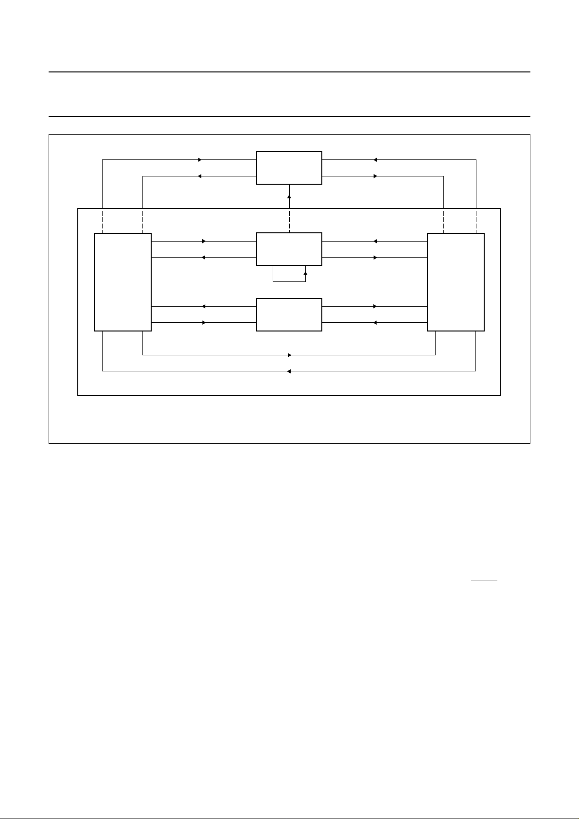
In this state conversation is possible. A number of sub-states (see Fig.23) exist:
• Handset state
• Hands-free state
• Hold state
• Mute state.
Depending on the diode option HMS the hold or the mute state is selected.
1998 Jan 08 24
Page 25
Philips Semiconductors Product specification
Versatile speech/dialler/ringer with
music-on-hold
handbook, full pagewidth
HANDSET
on-hook
off-hook
[HOLD/MUTE]
[HOLD/MUTE] + HMS = off
STANDBY
on-hook + pin HOLD = LOW
HOLD
MUTE
[HOOK]
[HOOK] + off-hook
[HOOK] + on-hook
[HOLD/MUTE] + HMS = on[HOLD/MUTE] + HMS = on
on-hook
[HOLD/MUTE][HOLD/MUTE]
[HOLD/MUTE]
[HOLD/MUTE] + HMS = off
TEA1069; TEA1069A
[HOOK]
HANDSFREE
CONVERSATION
Fig.23 Conversation states.
• Handset state.
The conversation states are shown in Fig.23.
• Hands-free state.
In hands-free mode output HF becomes HIGH which
activates a TEA1093/1094 hands-free IC. This state can
be reached from standby state and from the handset
state as follows:
– the [HOOK] key is pressed during standby mode
– the [HOOK] key is pressed during handset state is
lifted, then when the handset is put on the cradle the
set stays in the hands-free mode.
The set leaves the hands-free mode and output HF
becomes LOW when:
– the [HOOK] key is pressed and the handset is on the
cradle, the set goes to the standby mode
– the [HOOK] key is pressed and the handset is lifted,
the set goes to the handset state.
The volume on the loudspeaker or buzzer, in hands-free
and ringer mode, can be controlled in four levels using
the [VOL+] and [VOL−] keys.
MBH211
The hands-free volume can be changed according to
Fig.24.
• Hold state.
The hold state is entered when the [HOLD/MUTE] key is
pressed (diode HMS = on). This state can be entered
either from handset state or from hands-free state. Upon
entering this state outputs HF and MUTE become LOW.
In hold state a music-on-hold melody is generated by
output TONE. Pin MOH/DMO is HIGH (diode
GOS = off) during this state. This signal can be used to
adjust the volume of the TONE pin. SinceMUTE is LOW
the TONE output is transmitted to the telephone line.
As long as the TEA1069 and TEA1069A are in this state
the HOLD input pin is tested.
The set leaves the hold state when:
– [HOLD/MUTE] is pressed, the set returns to either the
handset or hands-free state
– the HOLD input becomes LOW, now the TEA1069
and TEA1069A return to the standby state.
1998 Jan 08 25
Page 26
Philips Semiconductors Product specification
Versatile speech/dialler/ringer with
music-on-hold
• Mute state.
When the [HOLD/MUTE] key is pressed (HMS = off) the
mute state is entered and MUTE becomes LOW.
In mute state a music-on-hold melody is generated by
output TONE. Pin MOH/DMO is HIGH (diode
GOS = off) during this state.
This signal can be used to adjust the volume of the
TONE pin. Since MUTE is LOW the TONE output is
transmitted to the telephone line. The mute state is left
when:
– [HOLD/MUTE] is pressed, set returns to either
handset- or hands-free state
– a dial action is started.
handbook, halfpage
[
VOL
+]
HIGHEST
(1)
TEA1069; TEA1069A
However when keying-in is much faster then dialling-out,
then the 32 digit dialling register will overflow. When this
occurs the dialling is stopped and the error beep will be
generated.
There are two dial modes: pulse dialling and tone dialling.
The initial dialling mode is determined by option PTS.
The state machine which controls the dial mode is shown
in Fig.25.
handbook, halfpage
PTS = on PTS = off
PULSE DIALLING
[
RECALL
[*/T ]
] + PTS = on
TONE DIALLING
MBH213
[
+]
VOL
HIGH
+]
VOL
LOW
[
+]
VOL
LOWEST
(1) VOL1 = HIGH, VOL2 = HIGH.
(2) VOL1 = LOW, VOL2 = HIGH.
(3) VOL1 = HIGH, VOL2 = LOW.
(4) VOL1 = LOW, VOL2 = LOW.
VOL
[
VOL
[
VOL
[
VOL
−][
(2)
−][
(3)
−]
(4)
−]
MBH212
Fig.24 Volume control state machine.
Dialling state
During the dial-keys entries the TEA1069 and TEA1069A
start immediately with transmission of the digit(s); the
minimum transmission time is unaffected by the speed of
the entry. Transmission continues as long as further
dial-keys entries have to be processed.
Fig.25 Dialling mode state machine.
• Pulse dialling.
In this mode all valid keys are dialled by the pulse dialler.
When during pulse dialling key [∗/T] is pressed, the
TEA1069 and TEA1069A switch over to tone dialling
(mixed mode dialling). After the switch-over, valid keys
are dialled by the tone dialler. The temporary tone mode
is terminated by going on-hook or recall.
• Tone dialling.
The ICs convert valid keys into data for the on-chip
DTMF generator. Tones are transmitted via output
TONE with minimum tone burst/pause duration.
The maximum tone burst/pause duration is equal to the
key pressing/release time.
• Register recall (flash/earth).
The [RECALL] key will result in a flash or earth action.
• Access pause.
When the [PAUSE/LNR] button is not the first key
pressed, an access pause is entered for repertory or
redialling procedures. When an access pause is
executed MUTE is HIGH. During manual dialling no
access pauses are dialled.
• Last Number Redial (LNR).
If the first key pressed is the [PAUSE/LNR] button, the
number stored in the redial register is recalled and
transmitted. A maximum number of 32 digits can be
1998 Jan 08 26
Page 27

Philips Semiconductors Product specification
Versatile speech/dialler/ringer with
music-on-hold
accepted for last number redial. If this maximum is
reached the redial function is inhibited. During LNR
programmed access pauses are also dialled.
The [RECALL] key and the (in pulse dialling mode
allowed) tone switch key [∗/T] are also stored in LNR
memory.
• Notepad function.
In conversation state it is possible to store a number into
the LNR register, which may be dialled after an
on-hook/off-hook action. The procedure is as follows:
– press [STORE]
– press to-be-stored sequence of the digits [0] to [9],
[PAUSE/LNR], [∗/T] or [RECALL]
– press [STORE]
– press [PAUSE/LNR].
Memory recall state
Repertory numbers can be dialled-out after or before
entering manual dialling, last number redial and by
entering the memory locations in successive order.
The stored numbers can be dialled by the following
procedures:
• Press [MRC]
• Press one of the numeric keys [0] to [9], corresponding
to the memory location
or
• Press one of the direct memory keys ([M1] to [M10]).
Program state
The program mode can be entered from the conversation
(on-line) mode.
Pressing the [STORE] key in this state puts the TEA1069
and TEA1069A in the program mode. The program state
can be left by going on-hook (by putting the handset on the
cradle or pressing the [HOOK] key), the program mode is
interrupted and nothing is stored, or by ending the store
procedures resulting in a proper store of the programmed
item.
• Programming repertory numbers.
Storing of a new repertory number including access
pauses, tone switch and register recall can be done by
the following procedures:
– press [STORE]
– press to-be-stored sequence of the digits [0] to [9],
[PAUSE/LNR], [∗/T] or [RECALL]
– press [MRC]
TEA1069; TEA1069A
– press one of the numeric keys [0] to [9],
corresponding to the memory location
or
– press [STORE]
– press to-be-stored sequence of the digits [0] to [9],
[PAUSE/LNR], [∗/T] or [RECALL]
– press [M1] to [M10].
For storing the redial number in repertory use:
– press [STORE]
– press [PAUSE/LNR]
– press [MRC]
– press one of the numeric keys [0] to [9],
corresponding to the memory location
or
– press [STORE]
– press [PAUSE/LNR]
– press [M1] to [M10].
If the keyboard described in Fig.17 is selected by the
KBS diode option, repertory memory place
[M1] = [MRC] + [1] to [M10] = [MRC] + [0], thus the set
has 10 repertory numbers which can be selected via two
different ways.
If the keyboard described in Fig.19 is selected by the
KBS diode option repertory memory place
[MRC] + [0] to [MRC] + [9] and [M1], [M2] and [M3] are
different repertory numbers, thus this set has in total
13 repertory numbers.
• Memory overflow.
A maximum of 224 digits can be stored in the repertory
memories. When the maximum is reached, no keytone
is generated when trying to store more digits. The store
procedure is cancelled automatically.
• Clear repertory number.
Clearing a memory location is possible via the same
procedure as for storing a number, except no telephone
number is entered, thus one of the following sequences
must be used:
– press [STORE]
– press [MRC]
– press one of the numeric keys [0] to [9],
corresponding to the memory location
or
– press [STORE]
– press [M1] to [M10].
1998 Jan 08 27
Page 28
Philips Semiconductors Product specification
Versatile speech/dialler/ringer with
TEA1069; TEA1069A
music-on-hold
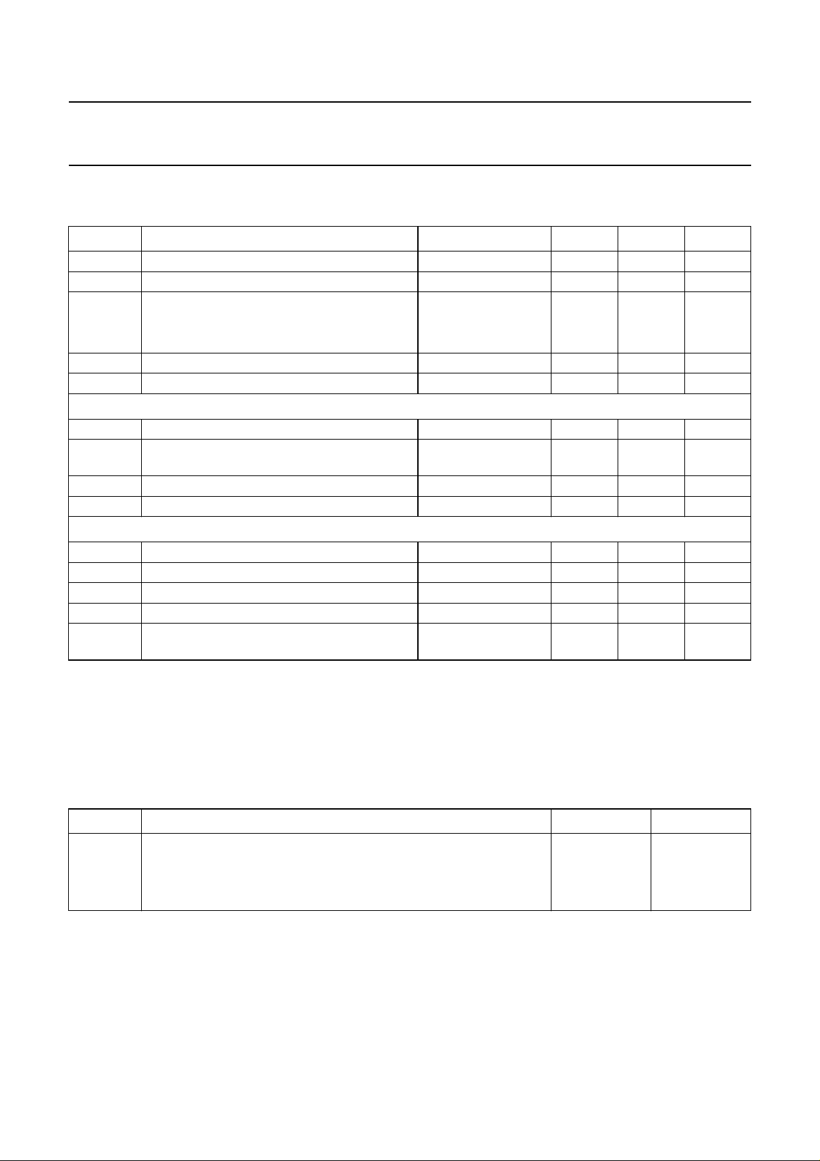
LIMITING VALUES
In accordance with the Absolute Maximum Rating System (IEC 134).
SYMBOL PARAMETER CONDITIONS MIN. MAX. UNIT
I
line
I
EE
P
tot
T
amb
T
stg
Speech part
V
LN
V
LN(R)
V
CC
V
i
Dialler/ringer part
V
DD
V
i
I
I
I
O
P
o
line current R9 = 20 Ω; note 1 − 140 mA
ground supply current through V
EE
− 50 mA
total power dissipation R9 = 20 Ω; note 2
TEA1069N − 770 mW
TEA1069H and TEA1069AH − 300 mW
operating ambient temperature −25 +70 °C
IC storage temperature −40 +125 °C
positive continuous line voltage − 12 V
repetitive line voltage during switch-on or line
− 13.2 V
interruption
input voltage on pin V
CC
− 12 V
input voltage on pins 1 to 7, 37, 38, 39, 41, 42 VEE− 0.7 VCC+ 0.7 V
supply voltage −0.7 +7 V
input voltages on pins 8 to 22, 24, 26 to 35 VEE− 0.7 VDD+ 0.7 V
DC input current on pins 8 to 22, 24, 26 to 35 −10 +10 mA
DC output current on pins 8 to 22, 24, 26 to 35 −10 +10 mA
power dissipation per output on pins 8 to 22,
− 30 mW
24, 26 to 35
Notes
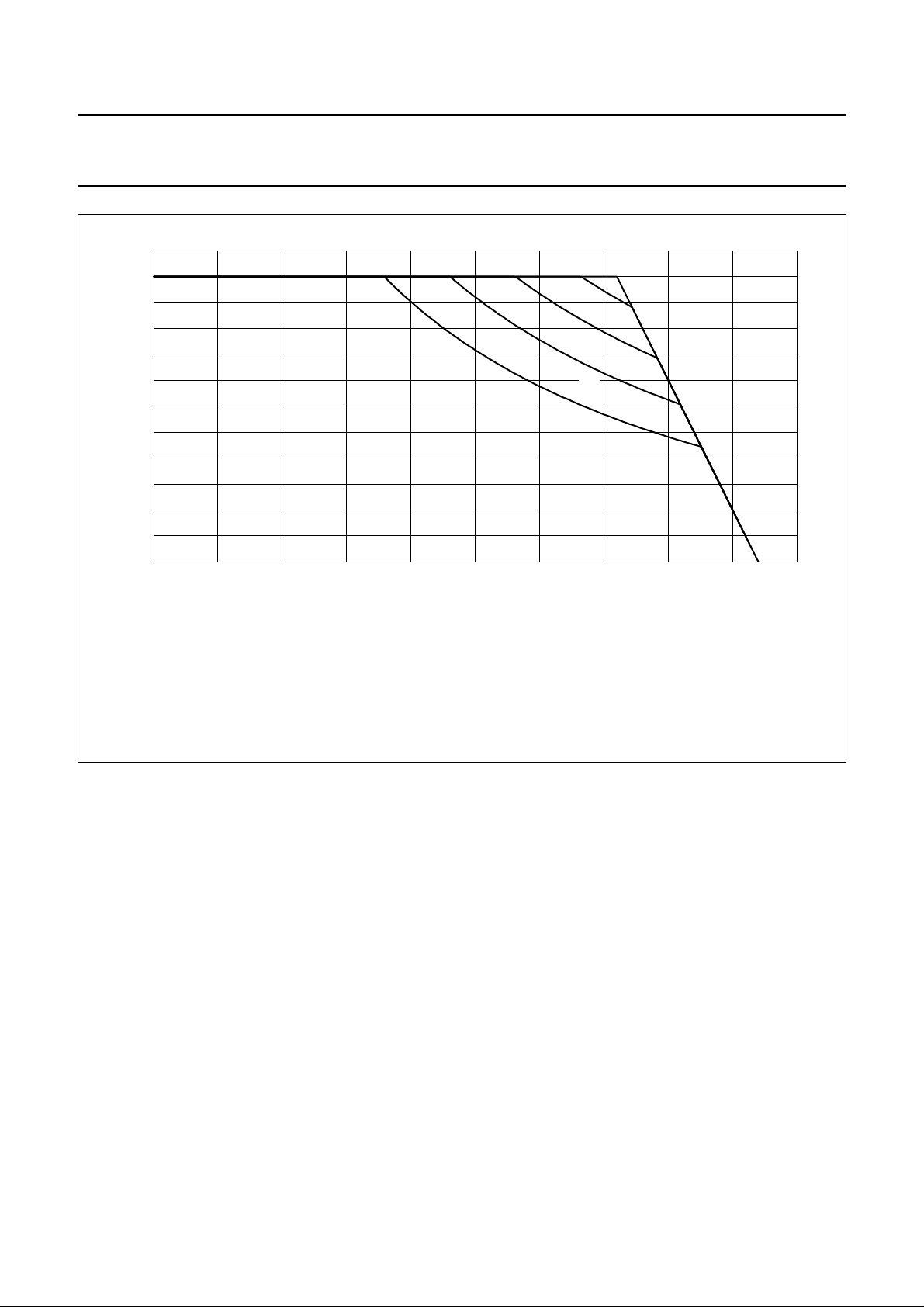
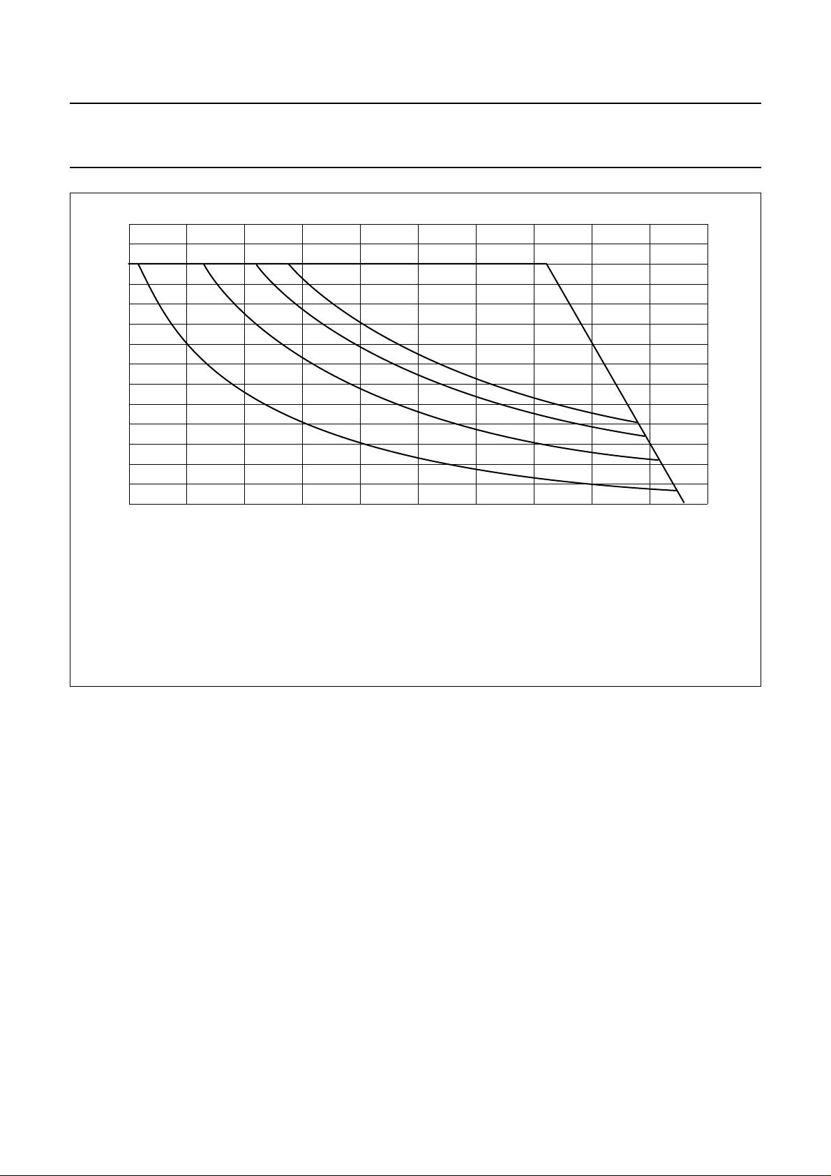
1. Mostly dependent on the maximum required T
and on the voltage between LN and SLPE (see Fig.26 for
amb
TEA1069N or Fig.27 for TEA1069H and TEA1069AH).
2. Calculated for the maximum specified ambient temperature (T
=70°C, see also Fig.26 for TEA1069N or Fig.27
amb
for TEA1069H and TEA1069AH).
THERMAL CHARACTERISTICS
SYMBOL PARAMETER VALUE UNIT
R
th j-a
thermal resistance from junction to ambient in free air mounted on
glass epoxy board 28.5 × 19.1 × 1.5 mm
TEA1069N 63 K/W
TEA1069H and TEA1069AH 116 K/W
1998 Jan 08 28
Page 29
Philips Semiconductors Product specification
Versatile speech/dialler/ringer with
music-on-hold
150
handbook, full pagewidth
I
line
(mA)
130
110
90
70
50
30
23456
TEA1069; TEA1069A
(1)
(2)
(3)
(4)
78910
V
LN
− V
MGD376
SLPE
1211
(V)
(1) T
(2) T
(3) T
(4) T
Note: calculations based upon negligible dialler and ringer parts output power (null port sink current).
amb
amb
amb
amb
=40°C; P
=50°C; P
=60°C; P
=70°C; P
= 1200 mW.
tot
= 1050 mW.
tot
= 910 mW.
tot
= 770 mW.
tot
Fig.26 TEA1069N safe operating area.
1998 Jan 08 29
Page 30
Philips Semiconductors Product specification
Versatile speech/dialler/ringer with
music-on-hold
160
handbook, full pagewidth
I
line
(mA)
140
120
100
80
60
40
20
23456
TEA1069; TEA1069A
(1)
(2)
(3)
(4)
78910
V
LN
− V
MBH785
SLPE
1211
(V)
(1) T
(2) T
(3) T
(4) T
Note: calculations based upon negligible dialler and ringer parts output power (null port sink current).
amb
amb
amb
amb
=40°C; P
=50°C; P
=60°C; P
=70°C; P
= 665 mW.
tot
= 590 mW.
tot
= 460 mW.
tot
= 300 mW.
tot
Fig.27 TEA1069H and TEA1069AH safe operating area.
1998 Jan 08 30
Page 31
Philips Semiconductors Product specification
Versatile speech/dialler/ringer with
TEA1069; TEA1069A
music-on-hold
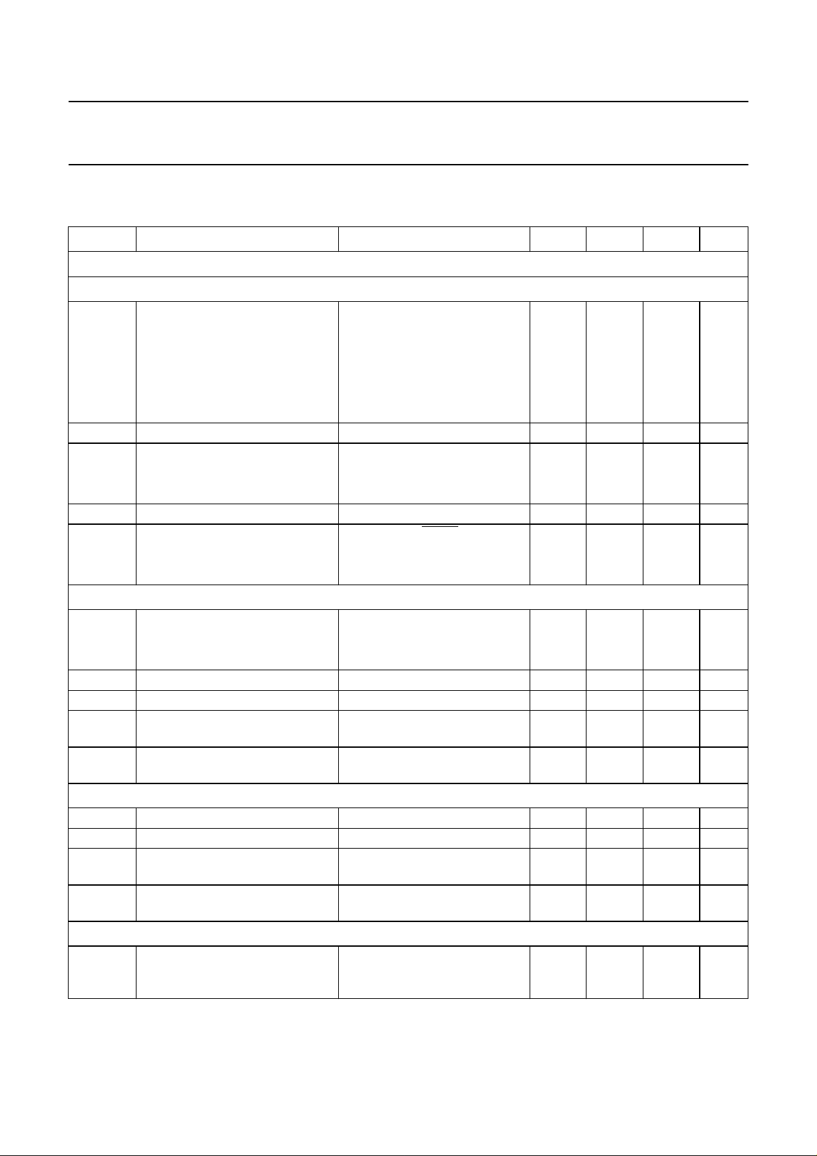
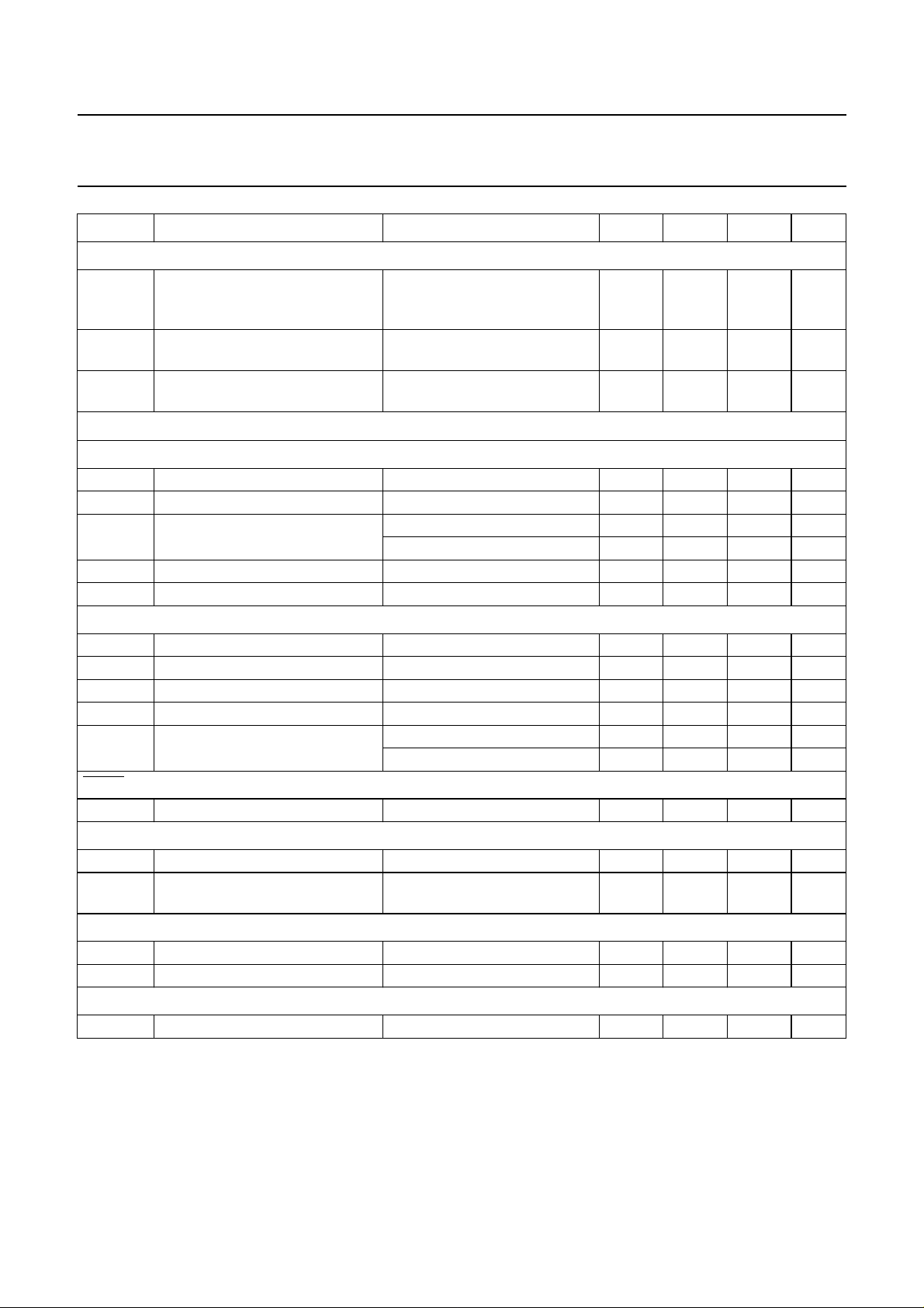
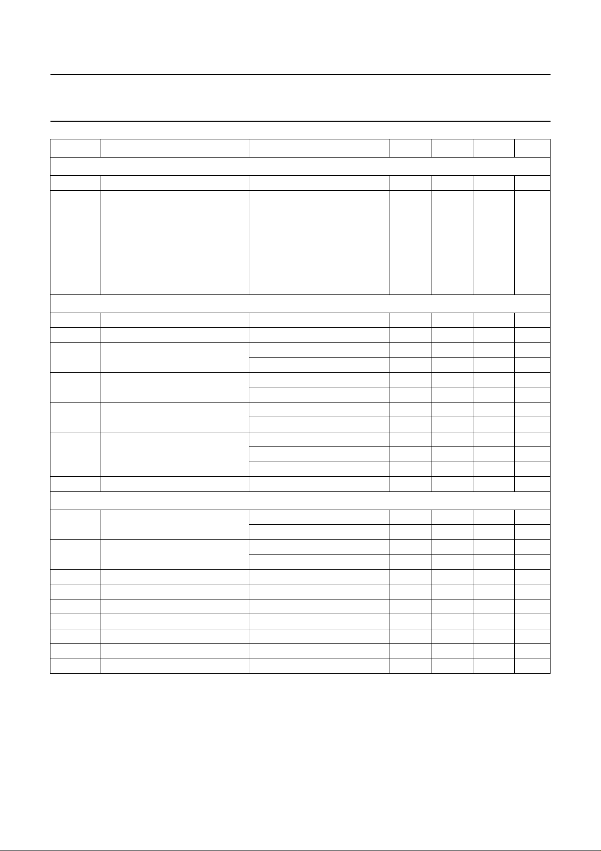
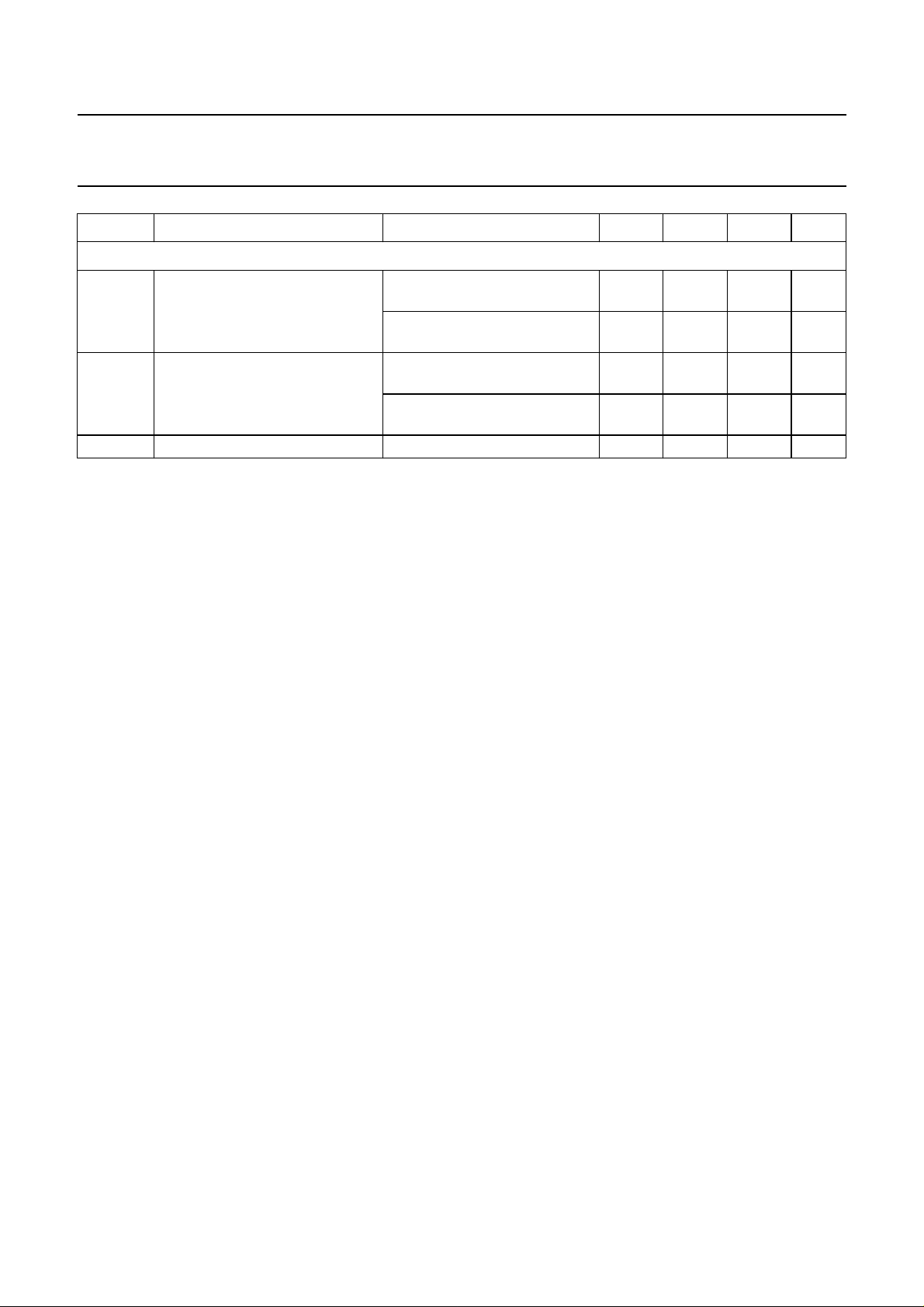
CHARACTERISTICS
= 11 to 140 mA; VEE= 0 V; f = 1 kHz; VDD=3V; f
I
line
SYMBOL PARAMETER CONDITIONS MIN. TYP. MAX. UNIT
Speech part
UPPLIES LN AND V
S
V
LN
voltage drop over circuit between
LN and V
∆V
/∆T variation with temperature I
LN
V
LN
voltage drop over circuit between
(PINS 40 AND 36)
CC
EE
MIC inputs open-circuit
line
I
line
LN and VEE with external resistor
R
VA
I
CC
V
CC
supply current VCC= 2.8 V − 0.9 1.35 mA
supply voltage available for
I
line
peripheral circuitry
MICROPHONE INPUTS MIC− AND MIC+ (PINS 3 AND 4)
Z
input impedance
i
differential between MIC− and MIC+ − 64 − kΩ
single-ended MIC− or MIC+ to V
CMRR common mode rejection ratio − 82 − dB
G
∆G
v
v(f)
voltage gain MIC+ or MIC− to LN I
gain variation with frequency
line
f = 300 and 3400 Hz −±0.2 − dB
referenced to 800 Hz
∆G
v(T)
gain variation with temperature
referenced to 25 °C
without R6; I
T
amb
DTMF INPUT (PIN 7)
input impedance − 20.7 − kΩ
Z
i
G
∆G
v
v(f)
voltage gain from DTMF to LN I
gain variation with frequency
line
f = 300 and 3400 Hz −±0.2 − dB
referenced to 800 Hz
∆G
v(T)
gain variation with temperature
referenced to 25 °C
I
T
line
amb
GAIN ADJUSTMENT INPUTS GAS1 AND GAS2 (PINS 41 AND 42)
∆G
v
transmitting amplifier gain
variation by adjustment of R7
between GAS1and GAS2
= 3.579545 MHz; T
xtal
I
=1mA − 1.6 − V
line
=4mA − 1.9 − V
I
line
I
= 15 mA 3.55 4.0 4.25 V
line
I
= 100 mA 4.9 5.7 6.5 V
line
I
= 140 mA −−7.5 V
line
=25°C; unless otherwise specified.
amb
=15mA −−0.3 − mV/K
=15mA
R
(LN to REG) = 68 kΩ− 3.5 − V
VA
R
(REG to SLPE) = 39 kΩ− 4.5 − V
VA
=15mA;MUTE = LOW
I
= 1.2 mA 2.2 2.7 − V
p
I
=0mA − 3.4 − V
p
EE
− 32 − kΩ
= 15 mA; R7 = 68 kΩ 50.5 52.0 53.5 dB
= 50 mA;
line
−±0.2 − dB
= −25 to +70 °C
= 15 mA; R7 = 68 kΩ 24.0 25.5 27.0 dB
=50mA;
−±0.2 − dB
= −25 to +70 °C
−8 − 0dB
1998 Jan 08 31
Page 32
Philips Semiconductors Product specification
Versatile speech/dialler/ringer with
TEA1069; TEA1069A
music-on-hold
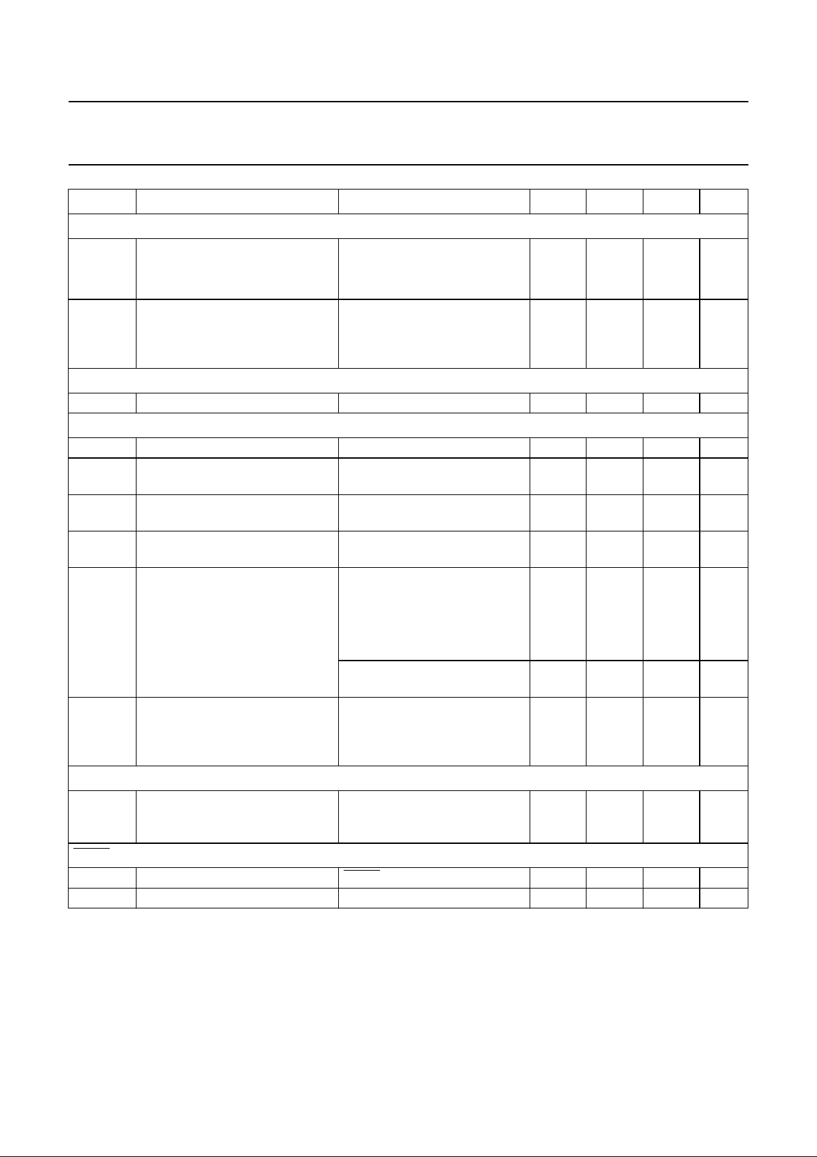
SYMBOL PARAMETER CONDITIONS MIN. TYP. MAX. UNIT
SENDING AMPLIFIER OUTPUT LN (PIN 40)
V
LN(rms)
V
no(rms)
RECEIVING AMPLIFIER INPUT IR (PIN 6)
input impedance − 21 − kΩ
Z
i
RECEIVING AMPLIFIER OUTPUT QR (PIN 1)
Z
output impedance − 4 −Ω
o
G
v
∆G
v(f)
∆G
v(T)
V
o(rms)
V
no(rms)
GAIN ADJUSTMENT INPUT GAR (PIN 2)
∆G
v
MUTE (PIN 35) GAIN REDUCTION
∆G
v
G
v
output voltage (RMS value) THD = 10%
I
=4mA − 0.8 − V
line
I
= 15 mA 1.7 2.3 − V
line
noise output voltage (RMS value) I
= 15 mA; R7 = 68 kΩ;
line
−−69 − dBmp
200 Ω between MIC− and
MIC+; psophometrically
weighted (P53 curve)
voltage gain from IR to QR I
= 15 mA; RL= 300 Ω
line
29.5 31 32.5 dB
(from pin 9 to pin 4)
gain variation with frequency
f = 300 and 3400 Hz −±0.2 − dB
referenced to 800 Hz
gain variation with temperature
referenced to 25 °C
without R6; I
T
= −25 and +70 °C
amb
= 50 mA;
line
−±0.2 − dB
output voltage (RMS value) THD = 2%; sine wave drive;
R4 = 100 kΩ; I
= 15 mA;
line
Ip=0mA
R
= 150 Ω 0.22 0.33 − V
L
= 450 Ω 0.3 0.48 − V
R
L
noise output voltage (RMS value) I
THD = 10%; R4 = 100 kΩ;
R
= 150 Ω; I
L
= 15 mA; R4 = 100 kΩ;
line
line
=4mA
− 15 − mV
− 50 −µV
IR open-circuit
psophometrically weighted
(P53 curve); RL= 300 Ω
receiving amplifier gain variation
−11 − 0dB
by adjustment of R4 between
GAR and QR
MIC+ or MIC− to LN MUTE = LOW − 70 − dB
voltage gain from DTMF to QR R4 = 100 kΩ; RL= 300 Ω− −17 − dB
1998 Jan 08 32
Page 33
Philips Semiconductors Product specification
Versatile speech/dialler/ringer with
TEA1069; TEA1069A
music-on-hold
SYMBOL PARAMETER CONDITIONS MIN. TYP. MAX. UNIT
AUTOMATIC GAIN CONTROL INPUT AGC (PIN 38)
∆G
v
gain control range (controlling the
gain from IR to QR and the gain
from MIC+, MIC− to LN)
I
lineH
highest line current for maximum
gain
I
lineL
lowest line current for minimum
gain
Dialler part
(PIN 25)
V
DD
V
DD
V
DD(MR)
I
DD
I
DD(MR)
V
POR
supply voltage 2.5 − 6.0 V
memory retention voltage 1.0 − 6.0 V
supply current DTMF generator off − 0.3 0.6 mA
memory retention current standby state, VDD= 1.8 V − 1.2 −µA
power-on reset trip level 1.5 2.0 2.5 V
INPUTS/OUTPUTS (PINS 9, 12 TO 21, 29 TO 34)
V
IL
V
IH
I
IL
I
OL
I
OH
LOW level input voltage 0 − 0.3V
HIGH level input voltage 0.7V
input leakage VEE<VI<V
port sink current LOW VDD=3V; VO= 0.4 V 0.7 8 − mA
port pull-up source current HIGH
(not valid for pin 33)
MUTE (PIN 35)
I
OL
port sink current LOW VDD=3V; VO= 0.4 V 0.7 8 − mA
OUTPUTS (PINS 8, 22, 26 TO 28)
I
OL
I
OH
port sink current LOW VDD=3V; VO= 0.4 V 0.7 8 − mA
port push-pull source current
HIGH
OSCILLATOR (PINS 10 AND 11)
g
m
R
f
transconductance 0.2 0.4 1.0 mA/V
feedback resistor 0.3 1.0 3.0 MΩ
CE/FDI (PIN 13)
t
rd
reset delay time − 280 − ms
R6 = 110 kΩ
−−5.8 − dB
(between AGC and VEE);
I
=70mA
line
R6 = 110 kΩ−23 − mA
R6 = 110 kΩ−61 − mA
DTMF generator on − 0.9 1.8 mA
V
DD
DD
− V
DD
DD
−1 − +1 µA
V
VDD=3V; VO= 2.7 V 10 20 −µA
=3V; VO=0V − 100 300 µA
V
DD
VDD=3V; VO= 2.6 V 0.7 4 − mA
1998 Jan 08 33
Page 34
Philips Semiconductors Product specification
Versatile speech/dialler/ringer with
TEA1069; TEA1069A
music-on-hold
SYMBOL PARAMETER CONDITIONS MIN. TYP. MAX. UNIT
KEYBOARD (PINS 14 TO 19 AND 29 TO 33)
t
d
t
ap
DP/FL
t
idp
t
holdover
t
interflash
t
m
t
b
t
rc
t
ea
TONE OUTPUT (PIN 24)
t
t
t
p
∆f/f frequency deviation −0.6 +0.6 %
V
HG(rms)
V
LG(rms)
V
DC
Z
output impedance − 100 500 Ω
o
V
G
THD total harmonic distortion −−25 − dB
keyboard debounce time − 20 − ms
access pause time
TEA1069 diodes APT off; APT2 off − 2 − s
diodes APT on; APT2 off − 4 − s
TEA1069A diodes APT off; APT2 off − 1 − s
diodes APT on; APT2 off − 4 − s
diodes APT off; APT2 on − 2 − s
diodes APT on; APT2 on − 3 − s
OUTPUT (PIN 20)
interdigit pause time − 840 − ms
mute hold-over time − 40 − ms
interflash hold-over time TEA1069 − 0 − ms
TEA1069A − 960 − ms
make time diode M/B off − 40 − ms
diode M/B on − 33 − ms
break time diode M/B off − 60 − ms
diode M/B on − 66 − ms
recall time using flash diode FES A off, FES B off − 100 − ms
diode FES A on, FES B off − 270 − ms
diode FES A off, FES B on − 600 − ms
recall time using earth diode FES A on, FES B on − 400 − ms
burst time diode TBT off − 100 − ms
diode TBT on − 85 − ms
pause time diode TBT off − 100 − ms
diode TBT on − 85 − ms
HGF voltage (RMS value) 158 181 205 mV
LGF voltage (RMS value) 125 142 160 mV
DC voltage level −
1
⁄2V
DD
− V
pre-emphasis of group 1.5 2.0 2.5 dB
1998 Jan 08 34
Page 35
Philips Semiconductors Product specification
Versatile speech/dialler/ringer with
TEA1069; TEA1069A
music-on-hold
SYMBOL PARAMETER CONDITIONS MIN. TYP. MAX. UNIT
Ringer part
f
ringL
f
ringH
t
rrd
ringer detection LOW frequency diode RFS off (TEA1069);
diode RFS on (TEA1069A)
diode RFS on (TEA1069);
diode RFS off (TEA1069A)
ringer detection HIGH frequency diode RFS off (TEA1069);
diode RFS on (TEA1069A)
diode RFS on (TEA1069);
diode RFS off (TEA1069A)
ringer response delay <1.5 frequency cycle −−150 ms
− 40 − Hz
− 29 − Hz
− 120 − Hz
− 146 − Hz
1998 Jan 08 35
Page 36
Philips Semiconductors Product specification
Versatile speech/dialler/ringer with
music-on-hold
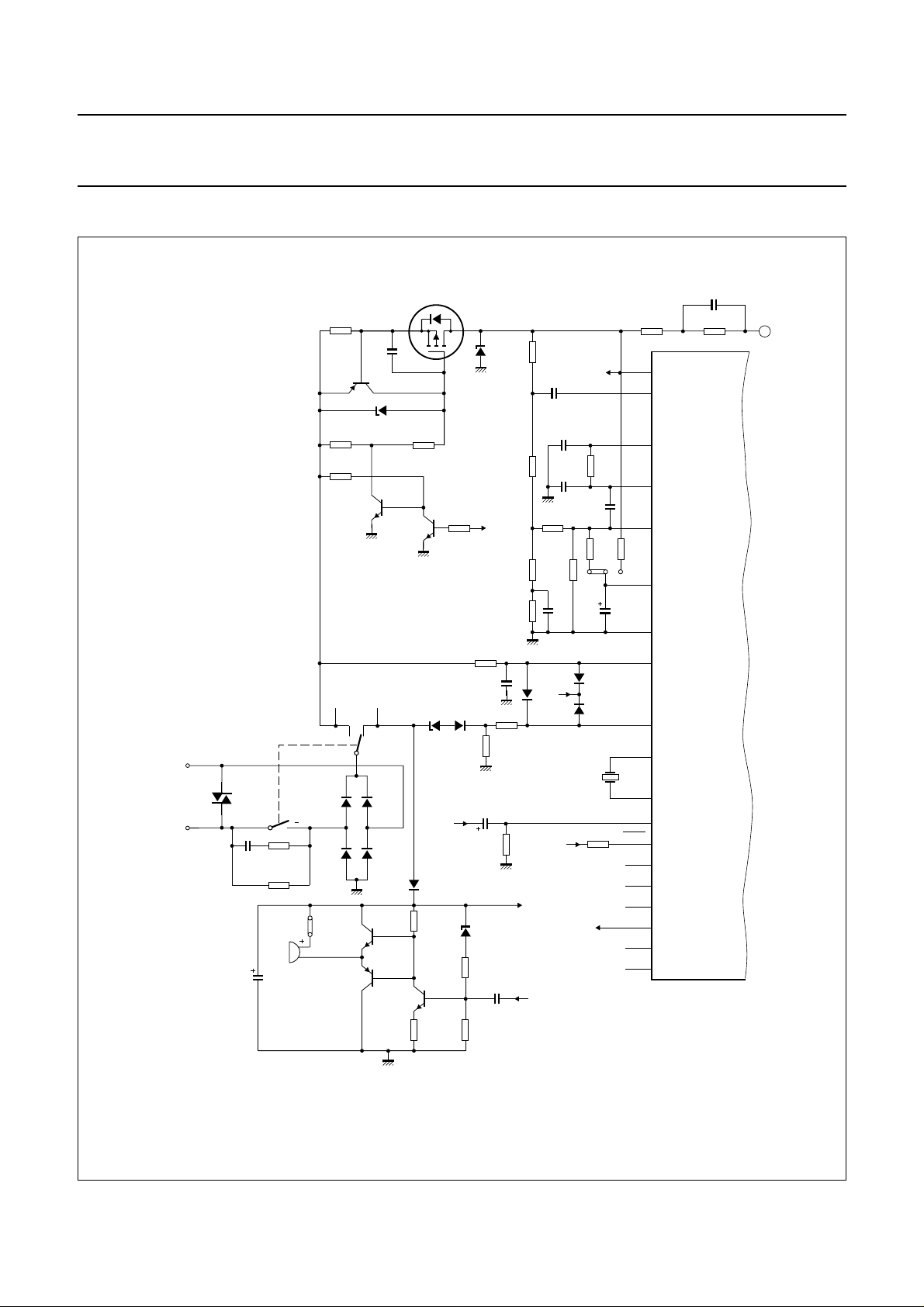
APPLICATION INFORMATION
handbook, full pagewidth
R20
3.9 Ω
C20
1 nF
TR2
BC558
BZX79C
(8.2 V)
R22
470 kΩ
R23
470 kΩ
TR3
BF420
speech ring
S1-1
D1
A−B/B−A
BR211_220
C30
1 µF
(250 V)
C31
22 µF
(35 V)
S1-2
R30
2.2 kΩ
R31
5.6 MΩ
40 V (p-p)
D2
BAS11
D4
BAS11
J4
BC546
H1
BC556
TR5
TR6
D3
BAS11
D5
BAS11
Z1
BC548C
TR7
BC548
470 kΩ
TR4
R21
Z3
BZX79C
(18 V)
1N4148
R32
100 kΩ
R34
1 kΩ
V
D10
DD
BSP254A
R24
2.2 MΩ
D6
1N4148
TR1
470 kΩ
2.2 nF
2.2 µF
(63 V)
R33
100 kΩ
R35
18 kΩ
Z2
BZX79C
(10 V)
3.92 kΩ
R40
C40
R42
470 kΩ
R41
100 kΩ
C41
Z4
BZX79C
(18 V)
C32
33 nF
R11
130 Ω
R12
820 Ω
R3
R43
470
kΩ
D7
1N4148
V
rr
TONE
R2
130
kΩ
C5
33 nF
C16
100 pF
C17
R8
390 Ω
R9
20 Ω
C12
220
nF
V
DD
3.58 MHz
V
CC
(1)
MOH/DMO
1 nF
100 pF
TEA1069; TEA1069A
C1b
LN
C6
J1
C3
D8
1N4148
D9
1N4148
X1
R44
56 kΩ
R7
27.4
kΩ
R60
100
kΩ
4.7 µF
(63 V)
CE/FDI
XTAL1
XTAL2
RESET
MOH/DMO
KT/EARTH
GAS2
GAS1
SLPE
R61
100
kΩ
REG
V
CSI
MUTE
VOL1
VOL2
HOLD
619 Ω
LN
IR
EE
HF
R1a
40 (36)
6 (44)
42 (38)
41 (37)
39 (35)DP/FL
37 (33)
23 (11, 18 and 23)
9 (3)
13 (7)
10 (4)
11 (5)
12 (6)
35 (31)
28 (24)
26 (21)
22 (17)
27 (22)
21 (16)
8 (2)
MBH214
R1b
TEA1069
A
Pin numbers in parenthesis refer to the TEA1069H and TEA1069AH.
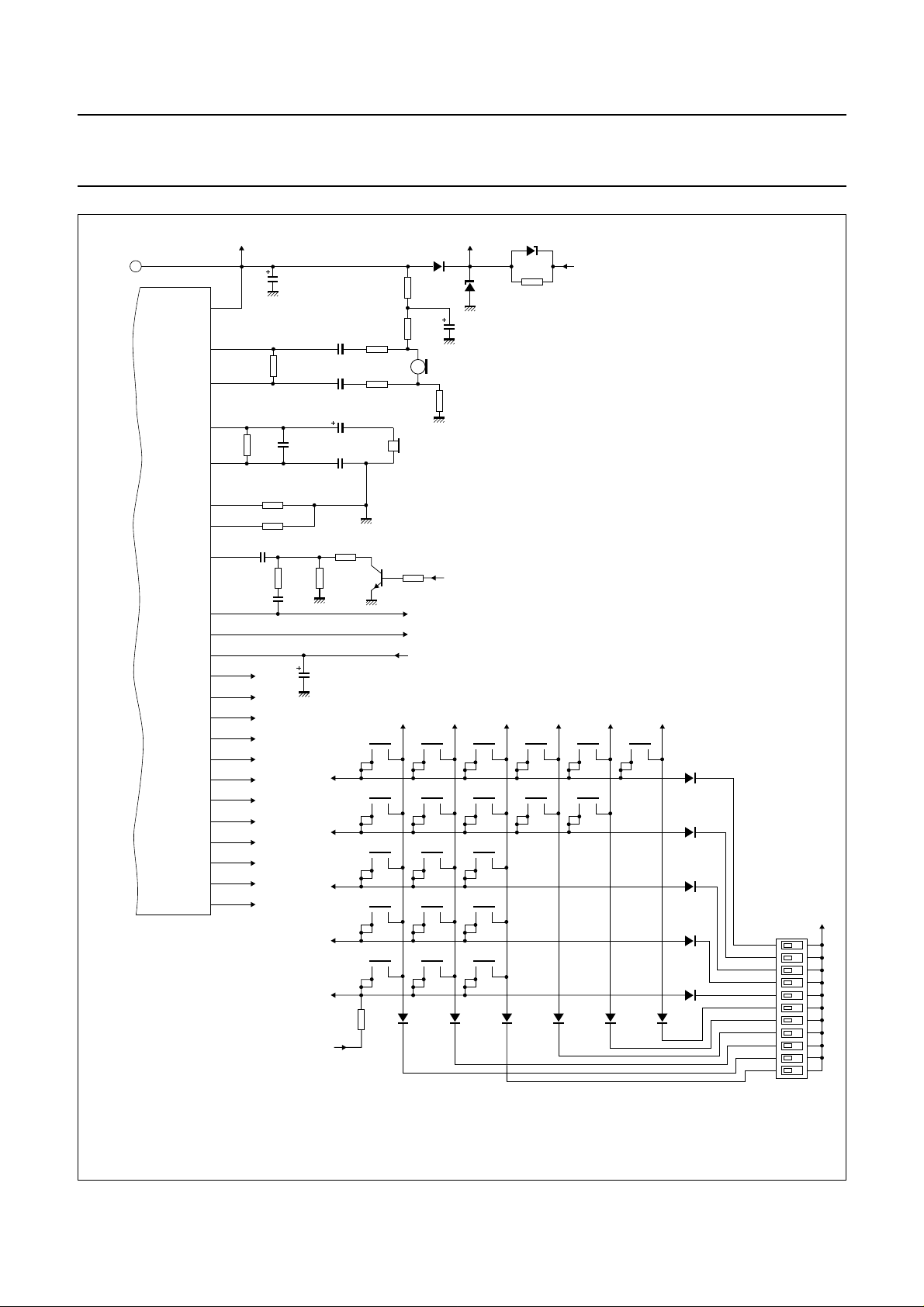
(1) Ringer supply voltage.
Fig.28 Basic application diagram (continued in Fig.29).
1998 Jan 08 36
Page 37
Philips Semiconductors Product specification
Versatile speech/dialler/ringer with
music-on-hold
handbook, full pagewidth
A
(32) 36
(41) 3
(42) 4
(39) 1
(40) 2
(43) 5
(34) 38
TEA1069
(19) 24
(15) 20
(20) 25
(30) 34
(25) 29
(26) 30
(27) 31
(28) 32
(29) 33
(14) 19
(13) 18
(12) 17
(10) 16
(9) 15
(8) 14
Pin numbers in parenthesis refer to the TEA1069H and TEA1069AH.
(1) Ringer supply voltage.
(2) Only on TEA1069A.
(1) 7
MBH215
V
V
CC
MIC−
MIC+
QR
GAR
STAB
AGC
DTMF
TONE
DP/FL
V
DD
DIODE
ROW1
ROW2
ROW3
ROW4
ROW5
COL1
COL2
COL3
COL4
COL5
COL6
CC
R4
68.1
kΩ
R5 3.65 kΩ
R6 110 kΩ
C14
100 nF
DIODE
ROW1
ROW2
ROW3
ROW4
ROW5
COL1
COL2
COL3
COL4
COL5
COL6
C1
100 µF
(25 V)
R14
8.2 kΩ
C4
560 pF
R45
10 kΩ
C44
100 nF
C42
470 µF
(10 V)
ROW1
ROW2
ROW3
ROW4
ROW5
V
DD
C18
150 nF
150 nF
C2 10 µF
(63 V)
C7 5.6 nF
R47 330 Ω
R46
3.65 kΩ
R50
680 kΩ
C19
R13
2.21 kΩ
R15
2.21 kΩ
TR8
BC548
1
S10
4
S16
7
S22
/T
*
S27
RECALL
S32
R10
3.32
kΩ
Fig.29 Basic application diagram (continued from Fig.28).
TEA1069; TEA1069A
V
BAT85
D11
Z5
R16
100 Ω
R17
100 Ω
R48
MOH
47 kΩ
TONE
DP/FL
V
DD
COL1 COL2 COL3 COL4 COL5 COL6
2
S11
5
S17
8
S23
0
S28
PAUSE/LNR
S33
D14
1N4148
DD
BZX79C
(5.6 V)
C15 47 µF
(25 V)
3
S12
6
S18
9
S24
#
S29
MUTE
S34
D15
1N4148
BZX79C (18 V)
Z6
R49
22.1 kΩ
STORE
S13
MRC
S19
D24
1N4148
V
M1
M3
D16
1N4148
rr
S14
S20
(1)
M2
S15
D17
1N4148
D19
1N4148
D20
1N4148
D21
1N4148
D22
1N4148
D23
1N4148
D18
1N4148
FES A
FES B
GOS
HMS
APT2
TBT
KBS
PTS
APT
RFS
M/B
DIODE
S2
1
2
3
4
5
6
7
8
9
10
(2)
11
1998 Jan 08 37
Page 38
Philips Semiconductors Product specification
Versatile speech/dialler/ringer with
music-on-hold
PACKAGE OUTLINES
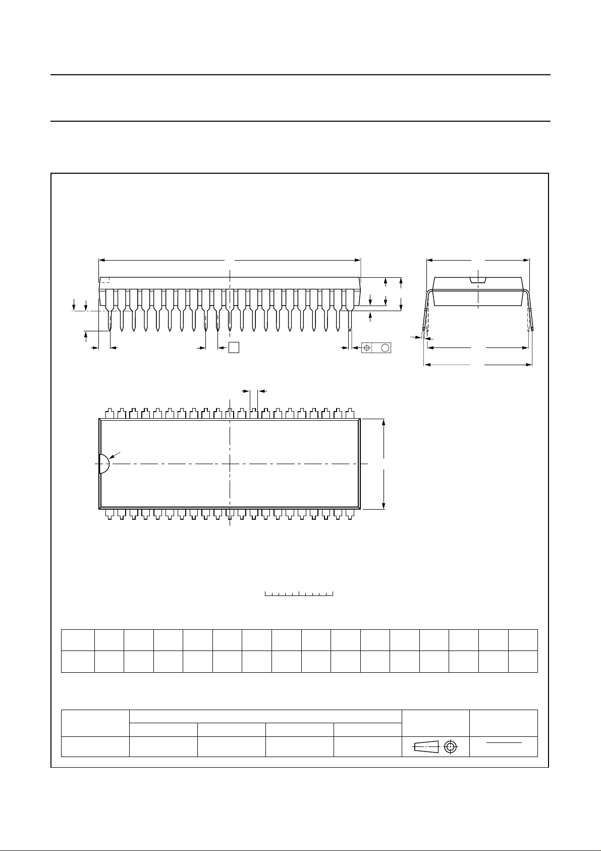
SDIP42: plastic shrink dual in-line package; 42 leads (600 mil)
D
seating plane
L
Z
e
TEA1069; TEA1069A
SOT270-1
M
E
A
2
A
A
1
w M
b
1
c
(e )
M
1
H
42
pin 1 index
1
DIMENSIONS (mm are the original dimensions)
A
A
A
UNIT b
mm
max.
5.08 0.51 4.0
12
min.
max.
b
1.3
0.8
0.53
0.40
b
22
E
21
0 5 10 mm
scale
cEe M
1
0.32
0.23
(1) (1)
D
38.9
38.4
14.0
13.7
1
L
M
E
3.2
15.80
2.9
15.24
17.15
15.90
e
w
H
0.181.778 15.24
Z
max.
1.73
(1)
Note
1. Plastic or metal protrusions of 0.25 mm maximum per side are not included.
OUTLINE
VERSION
SOT270-1
IEC JEDEC EIAJ
REFERENCES
1998 Jan 08 38
EUROPEAN
PROJECTION
ISSUE DATE
90-02-13
95-02-04
Page 39
Philips Semiconductors Product specification
Versatile speech/dialler/ringer with
TEA1069; TEA1069A
music-on-hold
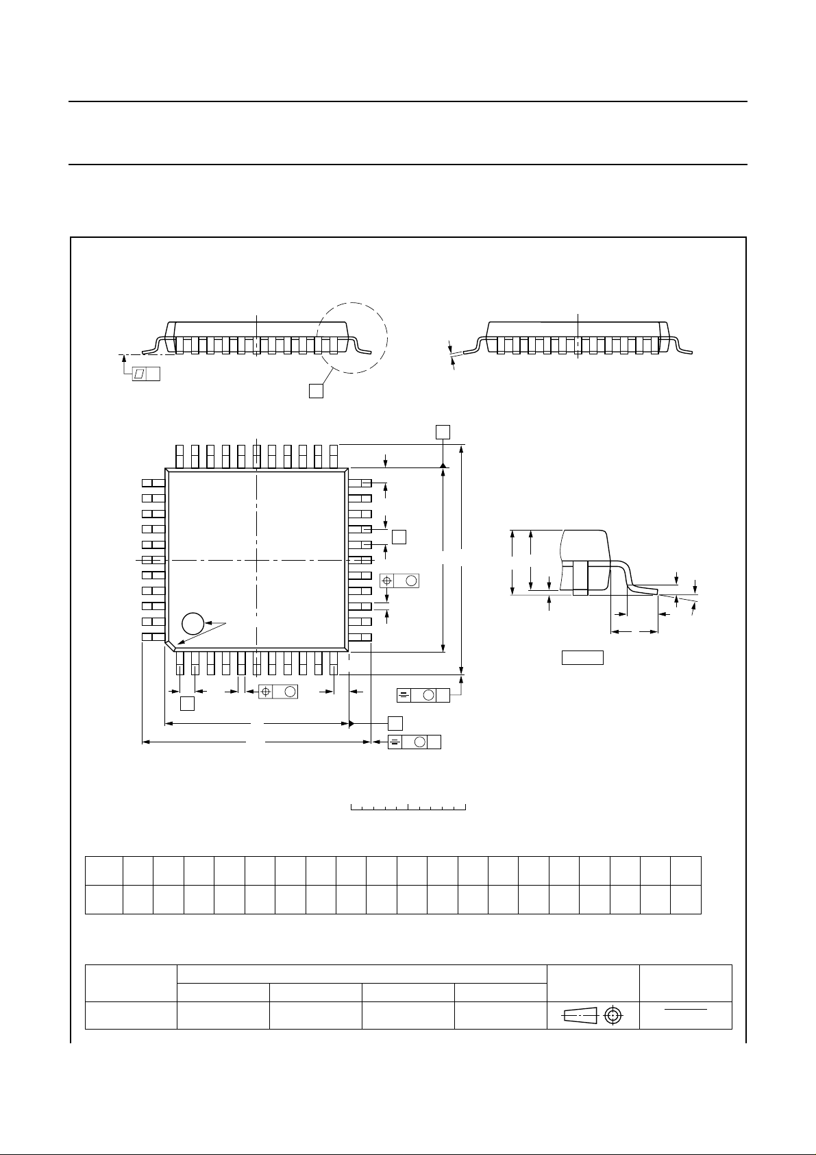
QFP44: plastic quad flat package; 44 leads (lead length 1.3 mm); body 10 x 10 x 1.75 mm
c
y
X
A
33 23
34
22
Z
E
SOT307-2
e
w M
b
p
pin 1 index
44
1
w M
b
0.25
p
D
H
D
cE
p
0.40
0.25
0.20
10.1
0.14
D
9.9
e
DIMENSIONS (mm are the original dimensions)
mm
A
max.
2.10
0.25
0.05
1.85
1.65
UNIT A1A2A3b
Note
1. Plastic or metal protrusions of 0.25 mm maximum per side are not included.
12
11
Z
D
B
v M
0 2.5 5 mm
scale
(1)
(1) (1)(1)
eH
H
10.1
9.9
12.9
0.8 1.3
12.3
v M
D
H
E
A
B
E
12.9
12.3
E
LL
0.95
0.55
A
p
A
2
A
1
detail X
Z
D
0.15 0.10.15
1.2
0.8
(A )
3
L
p
L
Zywv θ
E
1.2
0.8
θ
o
10
o
0
OUTLINE
VERSION
SOT307-2
IEC JEDEC EIAJ
REFERENCES
1998 Jan 08 39
EUROPEAN
PROJECTION
ISSUE DATE
95-02-04
97-08-01
Page 40

Philips Semiconductors Product specification
Versatile speech/dialler/ringer with
music-on-hold
SOLDERING
Introduction
There is no soldering method that is ideal for all IC
packages. Wave soldering is often preferred when
through-hole and surface mounted components are mixed
on one printed-circuit board. However, wave soldering is
not always suitable for surface mounted ICs, or for
printed-circuits with high population densities. In these
situations reflow soldering is often used.
This text gives a very brief insight to a complex technology.
A more in-depth account of soldering ICs can be found in
“IC Package Databook”
our
SDIP
SOLDERING BY DIPPING OR BY WA VE
The maximum permissible temperature of the solder is
260 °C; solder at this temperature must not be in contact
with the joint for more than 5 seconds. The total contact
time of successive solder waves must not exceed
5 seconds.
The device may be mounted up to the seating plane, but
the temperature of the plastic body must not exceed the
specified maximum storage temperature (T
printed-circuit board has been pre-heated, forced cooling
may be necessary immediately after soldering to keep the
temperature within the permissible limit.
R
EPAIRING SOLDERED JOINTS
Apply a low voltage soldering iron (less than 24 V) to the
lead(s) of the package, below the seating plane or not
more than 2 mm above it. If the temperature of the
soldering iron bit is less than 300 °C it may remain in
contact for up to 10 seconds. If the bit temperature is
between 300 and 400 °C, contact may be up to 5 seconds.
QFP
REFLOW SOLDERING
Reflow soldering techniques are suitable for all QFP
packages.
The choice of heating method may be influenced by larger
plastic QFP packages (44 leads, or more). If infrared or
vapour phase heating is used and the large packages are
not absolutely dry (less than 0.1% moisture content by
weight), vaporization of the small amount of moisture in
them can cause cracking of the plastic body. For more
information, refer to the Drypack chapter in our
Reference Handbook”
(order code 9398 652 90011).
). If the
stg max
“Quality
(order code 9397 750 00192).
TEA1069; TEA1069A
Reflow soldering requires solder paste (a suspension of
fine solder particles, flux and binding agent) to be applied
to the printed-circuit board by screen printing, stencilling or
pressure-syringe dispensing before package placement.
Several methods exist for reflowing; for example,
infrared/convection heating in a conveyor type oven.
Throughput times (preheating, soldering and cooling) vary
between 50 and 300 seconds depending on heating
method. Typical reflow peak temperatures range from
215 to 250 °C.
AVE SOLDERING
W
Wave soldering is not recommended for QFP packages.
This is because of the likelihood of solder bridging due to
closely-spaced leads and the possibility of incomplete
solder penetration in multi-lead devices.
CAUTION
Wave soldering is NOT applicable for all QFP
packages with a pitch (e) equal or less than 0.5 mm.
If wave soldering cannot be avoided, for QFP
packages with a pitch (e) larger than 0.5 mm, the
following conditions must be observed:
• A double-wave (a turbulent wave with high upward
pressure followed by a smooth laminar wave)
soldering technique should be used.
• The footprint must be at an angle of 45° to the board
direction and must incorporate solder thieves
downstream and at the side corners.
During placement and before soldering, the package must
be fixed with a droplet of adhesive. The adhesive can be
applied by screen printing, pin transfer or syringe
dispensing. The package can be soldered after the
adhesive is cured. Maximum permissible solder
temperature is 260 °C, and maximum duration of package
immersion in solder is 10 seconds, if cooled to less than
150 °C within 6 seconds. Typical dwell time is 4 seconds
at 250 °C. A mildly-activated flux will eliminate the need for
removal of corrosive residues in most applications.
R
EPAIRING SOLDERED JOINTS
Fix the component by first soldering two diagonallyopposite end leads. Use only a low voltage soldering iron
(less than 24 V) applied to the flat part of the lead. Contact
time must be limited to 10 seconds at up to 300 °C. When
using a dedicated tool, all other leads can be soldered in
one operation within 2 to 5 seconds between
270 and 320 °C.
1998 Jan 08 40
Page 41

Philips Semiconductors Product specification
Versatile speech/dialler/ringer with
TEA1069; TEA1069A
music-on-hold
DEFINITIONS
Data sheet status
Objective specification This data sheet contains target or goal specifications for product development.
Preliminary specification This data sheet contains preliminary data; supplementary data may be published later.
Product specification This data sheet contains final product specifications.
Limiting values
Limiting values given are in accordance with the Absolute Maximum Rating System (IEC 134). Stress above one or
more of the limiting values may cause permanent damage to the device. These are stress ratings only and operation
of the device at these or at any other conditions above those given in the Characteristics sections of the specification
is not implied. Exposure to limiting values for extended periods may affect device reliability.
Application information
Where application information is given, it is advisory and does not form part of the specification.
LIFE SUPPORT APPLICATIONS
These products are not designed for use in life support appliances, devices, or systems where malfunction of these
products can reasonably be expected to result in personal injury. Philips customers using or selling these products for
use in such applications do so at their own risk and agree to fully indemnify Philips for any damages resulting from such
improper use or sale.
1998 Jan 08 41
Page 42

Philips Semiconductors Product specification
Versatile speech/dialler/ringer with
music-on-hold
TEA1069; TEA1069A
NOTES
1998 Jan 08 42
Page 43

Philips Semiconductors Product specification
Versatile speech/dialler/ringer with
music-on-hold
TEA1069; TEA1069A
NOTES
1998 Jan 08 43
Page 44

Philips Semiconductors – a worldwide company
Argentina: see South America
Australia: 34 Waterloo Road, NORTH RYDE, NSW 2113,
Tel. +61 2 9805 4455, Fax. +61 2 9805 4466
Austria: Computerstr. 6, A-1101 WIEN, P.O. Box 213, Tel. +43 160 1010,
Fax. +43 160 101 1210
Belarus: Hotel Minsk Business Center, Bld. 3, r. 1211, Volodarski Str. 6,
220050 MINSK, Tel. +375 172 200 733, Fax. +375 172 200 773
Belgium: see The Netherlands
Brazil: seeSouth America
Bulgaria: Philips Bulgaria Ltd., Energoproject, 15thfloor,
51 James Bourchier Blvd., 1407 SOFIA,
Tel. +359 2 689 211, Fax. +359 2 689 102
Canada: PHILIPS SEMICONDUCTORS/COMPONENTS,
Tel. +1 800 234 7381
China/Hong Kong: 501 Hong Kong Industrial Technology Centre,
72 Tat Chee Avenue, Kowloon Tong, HONG KONG,
Tel. +852 2319 7888, Fax. +852 2319 7700
Colombia: see South America
Czech Republic: see Austria
Denmark: Prags Boulevard 80, PB 1919, DK-2300 COPENHAGEN S,
Tel. +45 32 88 2636, Fax. +45 31 57 0044
Finland: Sinikalliontie 3, FIN-02630 ESPOO,
Tel. +358 9 615800, Fax. +358 9 61580920
France: 51 Rue Carnot, BP317, 92156 SURESNES Cedex,
Tel. +33 1 40 99 6161, Fax. +33 1 40 99 6427
Germany: Hammerbrookstraße 69, D-20097 HAMBURG,
Tel. +49 40 23 53 60, Fax. +49 40 23 536 300
Greece: No. 15, 25th March Street, GR 17778 TAVROS/ATHENS,
Tel. +30 1 4894 339/239, Fax. +30 1 4814 240
Hungary: seeAustria
India: Philips INDIA Ltd, Band Box Building, 2nd floor,
254-D, Dr. Annie Besant Road, Worli, MUMBAI 400 025,
Tel. +91 22 493 8541, Fax. +91 22 493 0966
Indonesia: see Singapore
Ireland: Newstead, Clonskeagh, DUBLIN 14,
Tel. +353 1 7640 000, Fax. +353 1 7640 200
Israel: RAPAC Electronics, 7 Kehilat Saloniki St, PO Box 18053,
TEL AVIV 61180, Tel. +972 3 645 0444, Fax. +972 3 649 1007
Italy: PHILIPS SEMICONDUCTORS, Piazza IV Novembre 3,
20124 MILANO, Tel. +39 2 6752 2531, Fax. +39 2 6752 2557
Japan: Philips Bldg 13-37, Kohnan 2-chome, Minato-ku, TOKYO 108,
Tel. +81 3 3740 5130, Fax. +81 3 3740 5077
Korea: Philips House, 260-199 Itaewon-dong, Yongsan-ku, SEOUL,
Tel. +82 2 709 1412, Fax. +82 2 709 1415
Malaysia: No. 76 Jalan Universiti, 46200 PETALING JAYA, SELANGOR,
Tel. +60 3 750 5214, Fax. +60 3 757 4880
Mexico: 5900 Gateway East, Suite 200, EL PASO, TEXAS 79905,
Tel. +9-5 800 234 7381
Middle East: see Italy
Netherlands: Postbus 90050, 5600 PB EINDHOVEN, Bldg. VB,
Tel. +31 40 27 82785, Fax. +31 40 27 88399
New Zealand: 2 Wagener Place, C.P.O. Box 1041, AUCKLAND,
Tel. +64 9 849 4160, Fax. +64 9 849 7811
Norway: Box 1, Manglerud 0612, OSLO,
Tel. +47 22 74 8000, Fax. +47 22 74 8341
Philippines: Philips Semiconductors Philippines Inc.,
106 Valero St. Salcedo Village, P.O. Box 2108 MCC, MAKATI,
Metro MANILA, Tel. +63 2 816 6380, Fax. +63 2 817 3474
Poland: Ul. Lukiska 10, PL 04-123 WARSZAWA,
Tel. +48 22 612 2831, Fax. +48 22 612 2327
Portugal: see Spain
Romania: see Italy
Russia: Philips Russia, Ul. Usatcheva 35A, 119048 MOSCOW,
Tel. +7 095 755 6918, Fax. +7 095 755 6919
Singapore: Lorong 1, Toa Payoh, SINGAPORE 1231,
Tel. +65 350 2538, Fax. +65 251 6500
Slovakia: see Austria
Slovenia: see Italy
South Africa: S.A. PHILIPS Pty Ltd., 195-215 Main Road Martindale,
2092 JOHANNESBURG, P.O. Box 7430 Johannesburg 2000,
Tel. +27 11 470 5911, Fax. +27 11 470 5494
South America: Al. Vicente Pinzon, 173, 6th floor,
04547-130 SÃO PAULO, SP, Brazil,
Tel. +55 11 821 2333, Fax. +55 11 821 2382
Spain: Balmes 22, 08007 BARCELONA,
Tel. +34 3 301 6312, Fax. +34 3 301 4107
Sweden: Kottbygatan 7, Akalla, S-16485 STOCKHOLM,
Tel. +46 8 632 2000, Fax. +46 8 632 2745
Switzerland: Allmendstrasse 140, CH-8027 ZÜRICH,
Tel. +41 1 488 2686, Fax. +41 1 488 3263
Taiwan: Philips Semiconductors, 6F, No. 96, Chien Kuo N. Rd., Sec. 1,
TAIPEI, Taiwan Tel. +886 2 2134 2865, Fax. +886 2 2134 2874
Thailand: PHILIPS ELECTRONICS (THAILAND) Ltd.,
209/2 Sanpavuth-Bangna Road Prakanong, BANGKOK 10260,
Tel. +66 2 745 4090, Fax. +66 2 398 0793
Turkey: Talatpasa Cad. No. 5, 80640 GÜLTEPE/ISTANBUL,
Tel. +90 212 279 2770, Fax. +90 212 282 6707
Ukraine: PHILIPS UKRAINE, 4 Patrice Lumumba str., Building B, Floor 7,
252042 KIEV, Tel. +380 44 264 2776, Fax. +380 44 268 0461
United Kingdom: Philips Semiconductors Ltd., 276 Bath Road, Hayes,
MIDDLESEX UB3 5BX, Tel. +44 181 730 5000, Fax. +44 181 754 8421
United States: 811 East Arques Avenue, SUNNYVALE, CA 94088-3409,
Tel. +1 800 234 7381
Uruguay: see South America
Vietnam: see Singapore
Yugoslavia: PHILIPS, Trg N. Pasica 5/v, 11000 BEOGRAD,
Tel. +381 11 625 344, Fax.+381 11 635 777
For all other countries apply to: Philips Semiconductors,
International Marketing & Sales Communications, Building BE-p, P.O. Box 218,
5600 MD EINDHOVEN, The Netherlands, Fax. +31 40 27 24825
© Philips Electronics N.V. 1998 SCA57
All rights are reserved. Reproduction in whole or in part is prohibited without the prior written consent of the copyright owner.
The information presented in this document does not form part of any quotation or contract, is believed to be accurate and reliable and may be changed
without notice. No liability will be accepted by the publisher for any consequence of its use. Publication thereof does not convey nor imply any license
under patent- or other industrial or intellectual property rights.
Internet: http://www.semiconductors.philips.com
Printed in The Netherlands 417027/1200/04/pp44 Date of release: 1998 Jan 08 Document order number: 9397750 03133
 Loading...