

Page 1

INTEGRATED CIRCUITS
DATA SH EET
TEA0655
Dual Dolby B-type noise reduction
circuit for playback applications
Product specification
File under Integrated Circuits, IC01
September 1990
Page 2
Philips Semiconductors Product specification
Dual Dolby B-type noise reduction
TEA0655
circuit for playback applications
GENERAL DESCRIPTION
The TEA0655 is an integrated circuit that provides two Dolby* B-type noise reduction channels for playback applications
in car radios. The TEA0655 includes head and equalization amplifiers with electronically switched time constants.
The device will operate with power supplies in the range 9 to 15 volts, the output overload level increasing with an
increase in supply voltage. Current drain varies with supply voltage and noise reduction ON/OFF, therefore it is advisable
to use a regulated power supply or a supply with a long time constant.
FEATURES
• Dual noise reduction channels
• Head preamplifiers
• Equalization with electronically switched time constants
• Dolby reference level = 387.5 mV.
QUICK REFERENCE DATA
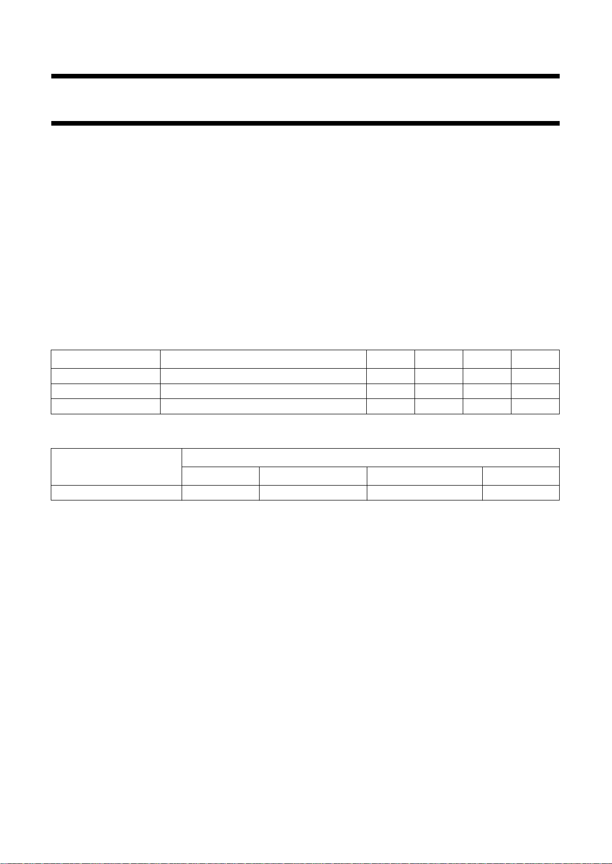
SYMBOL PARAMETER MIN. TYP. MAX. UNIT
V
CC
I
CC
(S+N)/N signal plus noise-to-noise ratio 78 84 − dB
supply voltage range 8 − 15 V
supply current − 20 25 mA
ORDERING AND PACKAGE INFORMATION
EXTENDED TYPE
NUMBER
TEA0655 20 DIL plastic SOT146 **
* Available only to licensees of Dolby Laboratories Licensing Corporation, San Francisco, CA94111, USA, from whom
licensing and application information must be obtained. Dolby is a registered trade-mark of Dolby Laboratories
Licensing Corporation.
** SOT146-1, August 1996.
PINS PIN POSITION MATERIAL CODE
PACKAGE
September 1990 2
Page 3
Philips Semiconductors Product specification
Dual Dolby B-type noise reduction circuit
for playback applications
TEA0655
September 1990 3
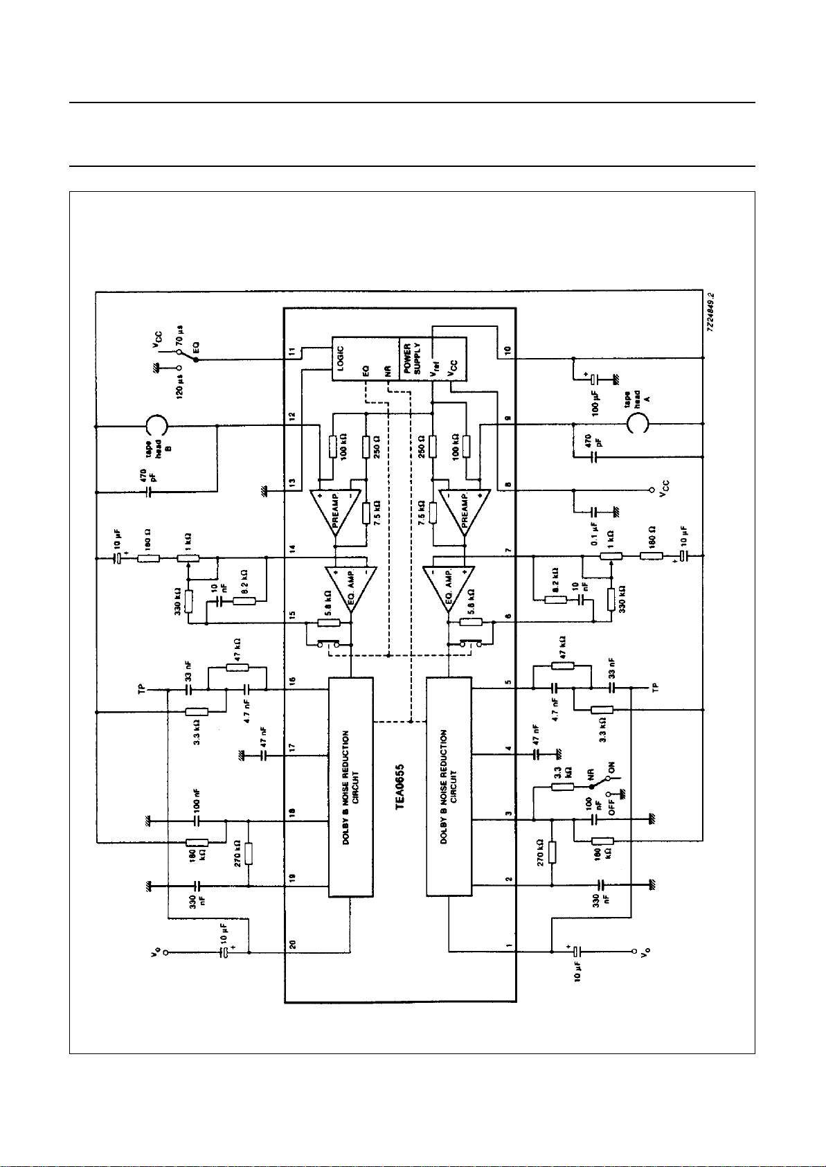
Fig.1 Block and application diagram.
Page 4
Philips Semiconductors Product specification
Dual Dolby B-type noise reduction circuit
TEA0655
for playback applications
FUNCTIONAL DESCRIPTION
Noise reduction is enabled when pin 3 is open-circuit and disabled when pin 3 is connected to GRD (pin 13) via a 3.3 kΩ
resistor (see Fig.1).
Pin 3 performs the functions of a logic input for noise reduction switching for both channels. It also provides smoothing
for the control signal in one channel. It is important that no voltage is applied to pin 3 when in the NR ON mode as this
will cause irregular noise reduction characteristics in the selected channel. Time constant switching is achieved by
applying a DC voltage to pin 11.
PINNING
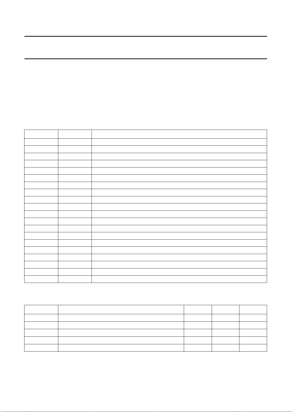
SYMBOL PIN DESCRIPTION
OUTA 1 output channel A
INTA 2 integrating filter channel A
CONTRA 3 control voltage channel A
HPA 4 high-pass filter channel A
SCA 5 side chain channel A
EQA 6 equalizing output channel A
EQFA 7 equalizing input channel A
V
CC
INA 9 input channel A
V
ref
SWEQ 11 equalizing switch
INB 12 input channel B
GRD 13 ground
EQFB 14 equalizing input channel B
EQB 15 equalizing output channel B
SCB 16 side chain channel B
HPB 17 high-pass filter channel B
CONTRB 18 control voltage channel B
INTB 19 integrating filter channel B
OUTB 20 output channel B
8 voltage supply
10 reference voltage
LIMITING VALUES
Limiting values in accordance with the Absolute Maximum Rating System (IEC 134)
SYMBOL PARAMETER MIN. MAX. UNIT
V
V
T
T
V
CC
I
amb
stg
es
supply voltage − 16 V
input voltage (pins 1 to 20) −0.3 V
operating ambient temperature range −40 +85 °C
storage temperature range −65 +150 °C
electrostatic handling
* Classification A: human body model; C = 100 pF, R = 1.5 kΩ, V = ≥ 2 kV; charge device model; C = 200 pF, R = 0 Ω,
V ≥ 500 V.
September 1990 4
CC
*
−−−
V
Page 5

Philips Semiconductors Product specification
Dual Dolby B-type noise reduction circuit
TEA0655
for playback applications
CHARACTERISTICS
= 10 V; f = 20 Hz to 20 kHz; T
V
CC
(pin 1 or 20); test circuit Fig.1; NR ON; EQ switch in the 70 µs position; unless otherwise specified.
SYMBOL PARAMETER CONDITIONS MIN. TYP. MAX. UNIT
V
I
CC
CC
supply voltage 8 10 15 V
supply current − 20 25 mA
channel matching NR OFF −0.5 − +0.5 dB
THD distortion 2nd and 3rd harmonic f = 1 kHz; 0 dB − 0.08 0.15 %
signal handling V
(S+N)/N signal-plus-noise to noise ratio
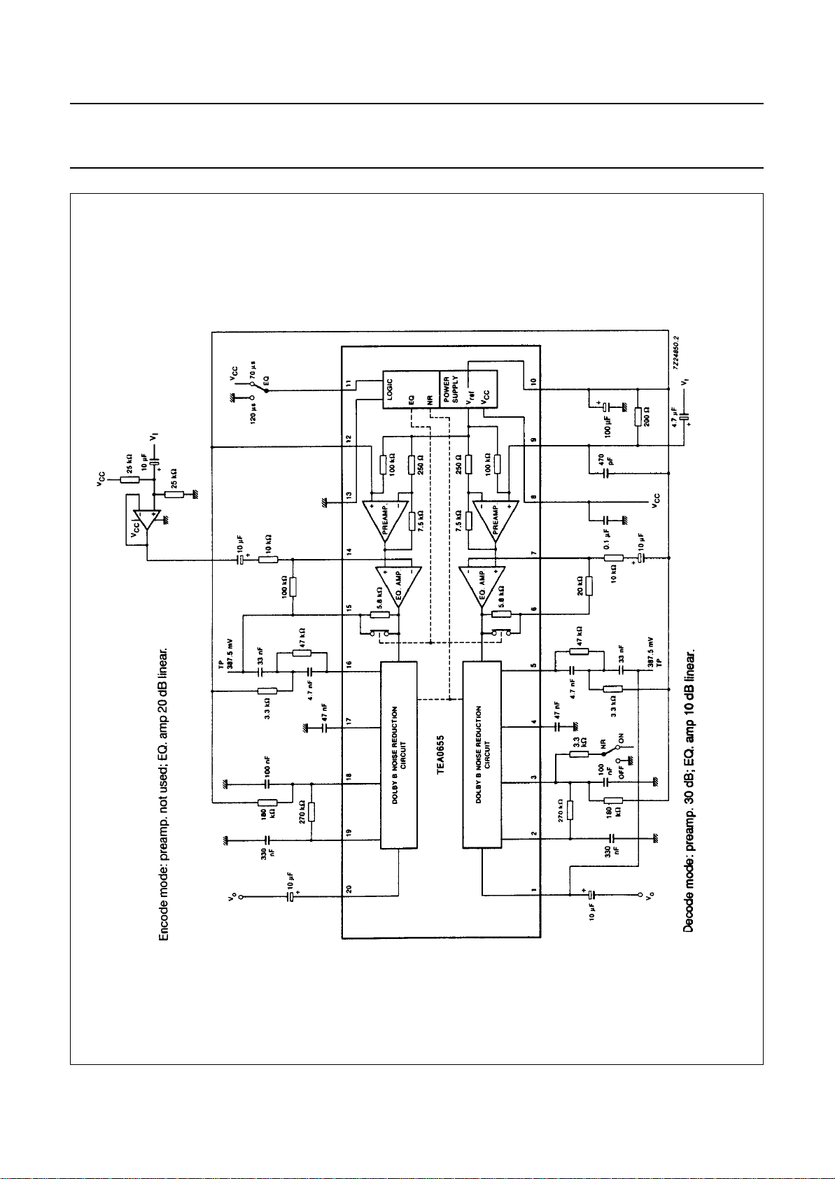
(see Fig.2; decode mode)
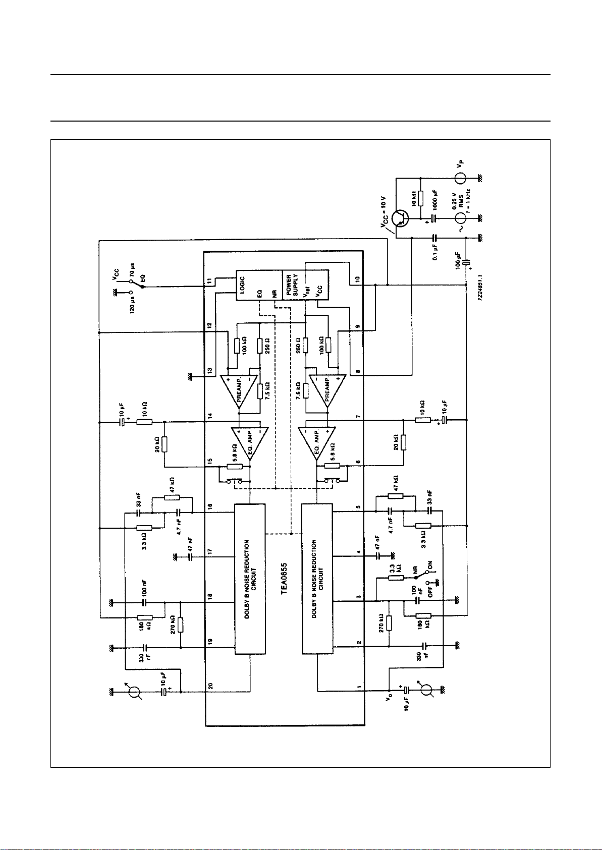
PSRR power supply ripple rejection f = 1 kHz; 250 mV;
= +25 °C; all levels referenced to 387.5 mV RMS (0 dB) at test point (TP)
amb
f = 10 kHz; +10 dB − 0.15 0.3 %
= 8 V; 1% distortion at
CC
12 15 − dB
1 kHz
internal gain 40 dB linear;
78 84 − dB
CCIR/ARM weighted
52 57 − dB
see Fig.3
α
CR
R
Lmin
G
V
V
off
I
B
R
EQ
R
I
frequency response measured
in encode mode see Fig.2
referenced to test point
note 1
f = 1 kHz; 0 dB −1.5 0 +1.5 dB
f = 1 kHz; −25 dB −17.8 −19.3 −20.8 dB
f = 0.2 kHz; −25 dB −22.9 −24.4 −25.9 dB
f = 5 kHz; −25 dB −18.1 −19.6 −21.1 dB
f = 10 kHz; −35 dB −24.4 −25.9 −27.4 dB
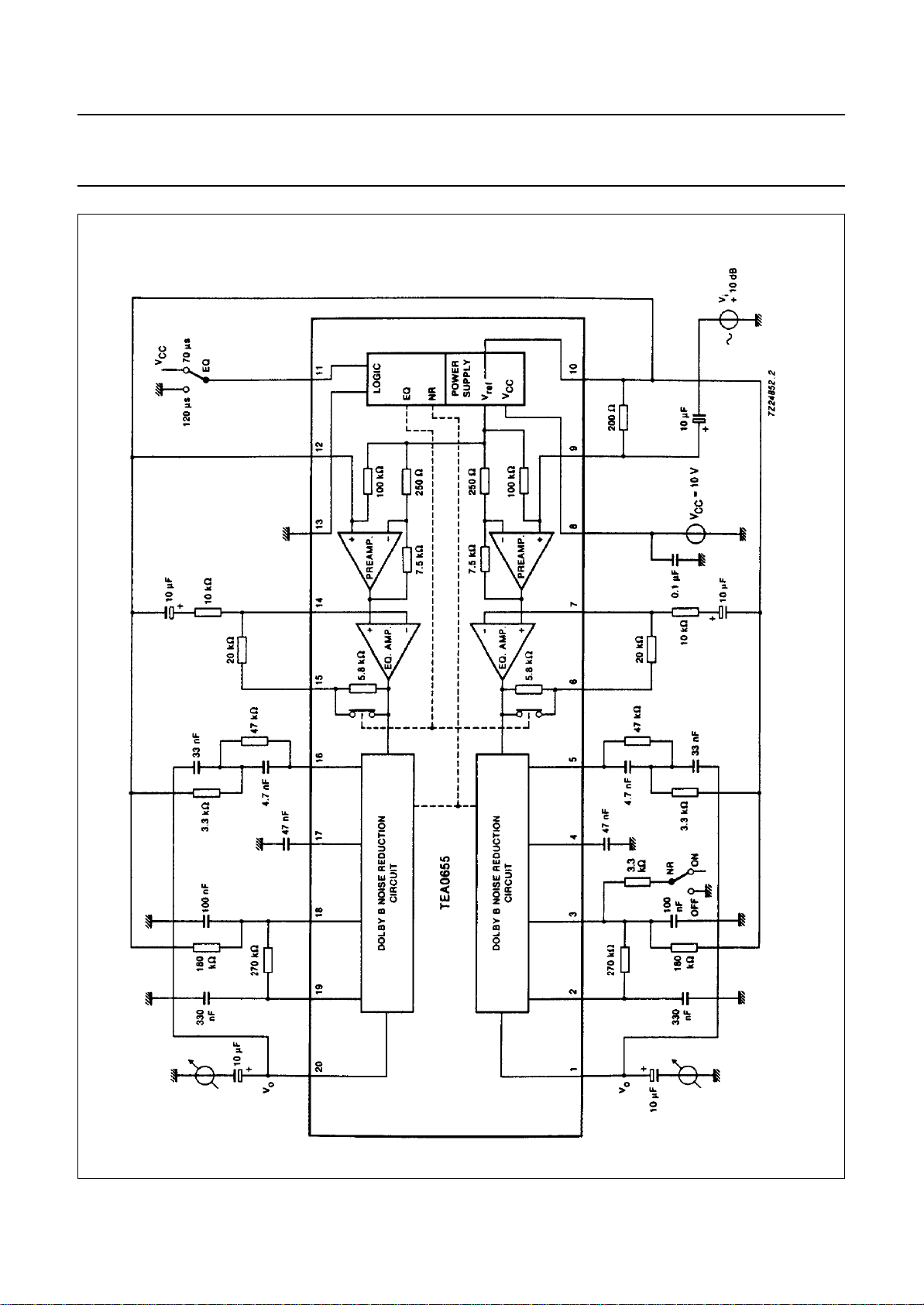
channel separation f = 1 kHz; see Fig.4 57 63 − dB
minimum load resistance on
12 dB; 1 kHz; 1% THD 10 −−kΩ
output (pins 1 and 20)
voltage gain (pin 9 to 7 or pin 12
1 kHz 29 30 31 dB
to 14)
input offset voltage − 2 − mV
input bias current − 0.1 0.4 µA
equalizing resistor 4.7 5.8 6.9 kΩ
input resistance pins 9 and 12 60 100 − kΩ
September 1990 5
Page 6
Philips Semiconductors Product specification
Dual Dolby B-type noise reduction circuit
TEA0655
for playback applications
SYMBOL PARAMETER CONDITIONS MIN. TYP. MAX. UNIT
A
V
Z
O
I
OGRD
I
OVCC
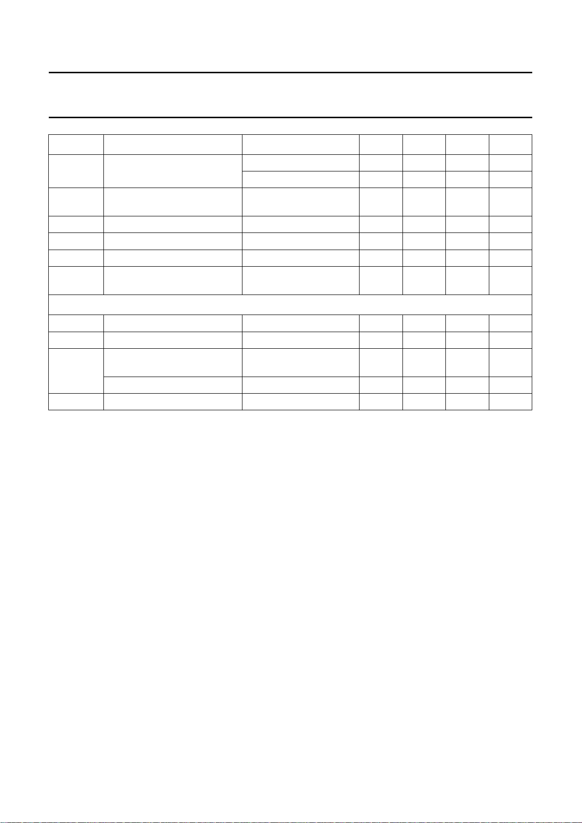
En equivalent input noise voltage
Switching thresholds
V
OFF
I
3
open loop gain pins 12/15 and
pins 9/6
DC output voltage pins 1 and 20 NR OFF with reference to
10 kHz 80 86 − dB
400 kHz 104 110 − dB
−−±0.15 V
/2
V
CC
output impedance − 50 70 Ω
DC output current capability to ground −−−2mA
to V
CC
NR OFF; unweighted;
(RMS value)
20 Hz to 20 kHz; R
= 0 Ω
S
NR switch OFF (pin 3) 0 − 0.2V
−−300 µA
− 0.7 1.4 µV
V
CC
NR switch ON − open −100 nA
equalizing (EQ) switch (pin 11)
0.5V
CC
− V
CC
V
at 70 µs
equalizing switch at 120 µs0−0.2V
I
11
input current −−−1µA
Note to the characteristics
1. Equals the corresponding decode mode cut with reference to test point level, see Fig.1.
CC
V
September 1990 6
Page 7
Philips Semiconductors Product specification
Dual Dolby B-type noise reduction circuit
for playback applications
TEA0655
September 1990 7
Fig.2 Test circuit for frequency response (channel B).
Page 8
Philips Semiconductors Product specification
Dual Dolby B-type noise reduction circuit
for playback applications
TEA0655
September 1990 8
Fig.3 Test circuit for power supply ripple rejection (PSRR).
Page 9
Philips Semiconductors Product specification
Dual Dolby B-type noise reduction circuit
for playback applications
TEA0655
).
CS
September 1990 9
Fig.4 Test circuit for channel separation (α
Page 10
Philips Semiconductors Product specification
Dual Dolby B-type noise reduction circuit
for playback applications
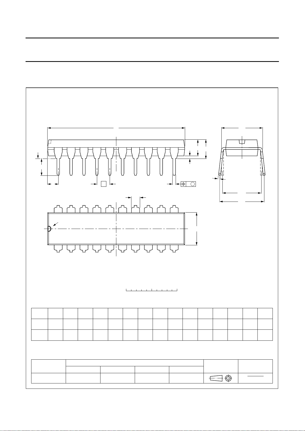
PACKAGE OUTLINE
DIP20: plastic dual in-line package; 20 leads (300 mil)
D
seating plane
L
Z
20
e
b
TEA0655
SOT146-1
M
E
A
2
A
A
1
w M
b
1
11
c
(e )
1
M
H
pin 1 index
1
0 5 10 mm
scale
DIMENSIONS (inch dimensions are derived from the original mm dimensions)
A
A
A
UNIT
inches
Note
1. Plastic or metal protrusions of 0.25 mm maximum per side are not included.
max.
mm
OUTLINE
VERSION
SOT146-1
1 2
min.
max.
1.73
1.30
0.068
0.051
IEC JEDEC EIAJ
SC603
b
b
1
0.53
0.38
0.021
0.015
0.36
0.23
0.014
0.009
REFERENCES
cD E e M
(1) (1)
26.92
26.54
1.060
1.045
6.40
6.22
0.25
0.24
E
10
(1)
M
e
L
1
3.60
8.25
3.05
7.80
0.14
0.32
0.12
0.31
EUROPEAN
PROJECTION
H
E
10.0
0.2542.54 7.62
8.3
0.39
0.010.10 0.30
0.33
ISSUE DATE
w
92-11-17
95-05-24
Z
max.
2.04.2 0.51 3.2
0.0780.17 0.020 0.13
September 1990 10
Page 11

Philips Semiconductors Product specification
Dual Dolby B-type noise reduction circuit
for playback applications
SOLDERING
Introduction
There is no soldering method that is ideal for all IC
packages. Wave soldering is often preferred when
through-hole and surface mounted components are mixed
on one printed-circuit board. However, wave soldering is
not always suitable for surface mounted ICs, or for
printed-circuits with high population densities. In these
situations reflow soldering is often used.
This text gives a very brief insight to a complex technology.
A more in-depth account of soldering ICs can be found in
“IC Package Databook”
our
Soldering by dipping or by wave
The maximum permissible temperature of the solder is
260 °C; solder at this temperature must not be in contact
with the joint for more than 5 seconds. The total contact
time of successive solder waves must not exceed
5 seconds.
(order code 9398 652 90011).
TEA0655
The device may be mounted up to the seating plane, but
the temperature of the plastic body must not exceed the
specified maximum storage temperature (T
printed-circuit board has been pre-heated, forced cooling
may be necessary immediately after soldering to keep the
temperature within the permissible limit.
Repairing soldered joints
Apply a low voltage soldering iron (less than 24 V) to the
lead(s) of the package, below the seating plane or not
more than 2 mm above it. If the temperature of the
soldering iron bit is less than 300 °C it may remain in
contact for up to 10 seconds. If the bit temperature is
between 300 and 400 °C, contact may be up to 5 seconds.
stg max
). If the
DEFINITIONS
Data sheet status
Objective specification This data sheet contains target or goal specifications for product development.
Preliminary specification This data sheet contains preliminary data; supplementary data may be published later.
Product specification This data sheet contains final product specifications.
Limiting values
Limiting values given are in accordance with the Absolute Maximum Rating System (IEC 134). Stress above one or
more of the limiting values may cause permanent damage to the device. These are stress ratings only and operation
of the device at these or at any other conditions above those given in the Characteristics sections of the specification
is not implied. Exposure to limiting values for extended periods may affect device reliability.
Application information
Where application information is given, it is advisory and does not form part of the specification.
LIFE SUPPORT APPLICATIONS
These products are not designed for use in life support appliances, devices, or systems where malfunction of these
products can reasonably be expected to result in personal injury. Philips customers using or selling these products for
use in such applications do so at their own risk and agree to fully indemnify Philips for any damages resulting from such
improper use or sale.
September 1990 11
 Loading...