

Page 1
TDS.11..
Vishay Telefunken
1 (9)
Rev. A1, 02-Jun-99
www.vishay .de • FaxBack +1-408-970-5600Document Number 83124
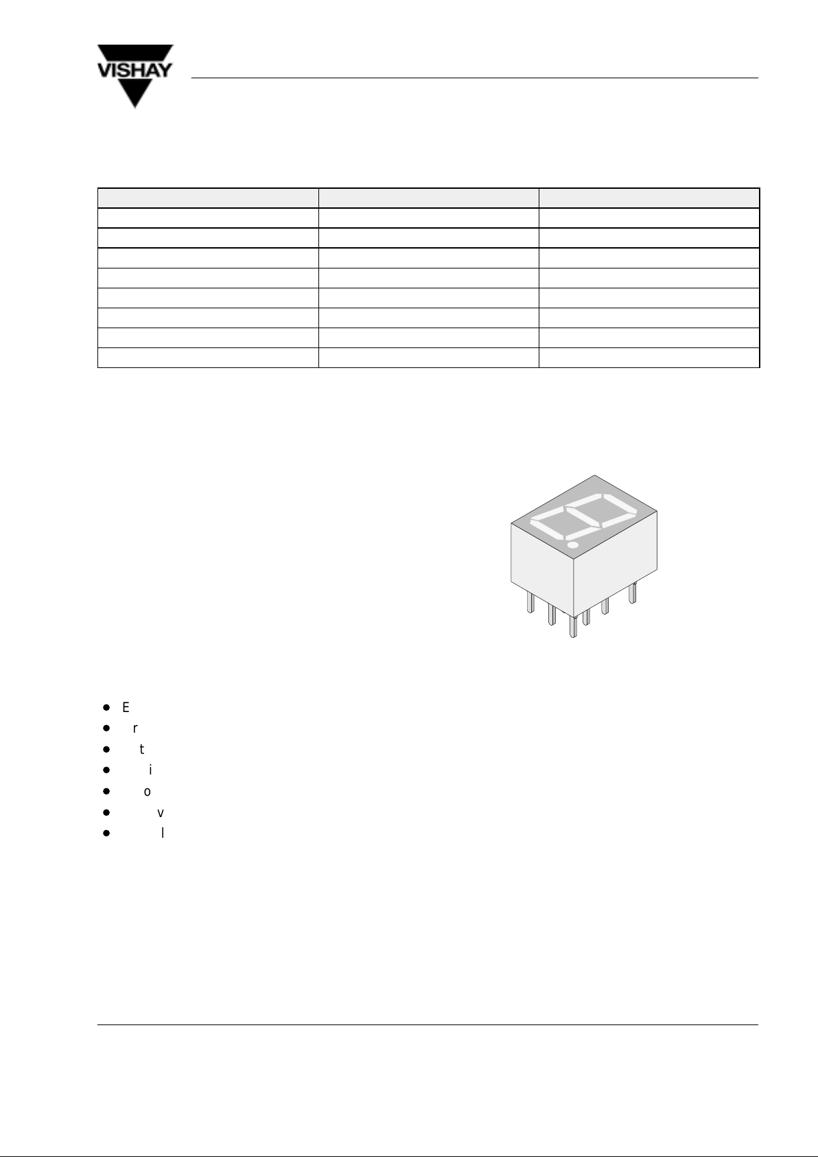
7 mm Seven Segment Display
Color Type Circuitry
Red TDSR115. Common anode
Red TDSR116. Common cathode
Orange red TDSO115. Common anode
Orange red TDSO116. Common cathode
Yellow TDSY115. Common anode
Yellow TDSY116. Common cathode
Green TDSG115. Common anode
Green TDSG116. Common cathode
Description
The TDS.11.. series are 7 mm character seven segment LED displays in a very compact package.
The displays are designed for a viewing distance up to
3 meters and available in four bright colors. The grey
package surface and the evenly lighted untinted segments provide an optimum on-off contrast.
All displays are categorized in luminous intensity
groups. That allows users to assemble displays with
uniform appearence.
Typical applications include instruments, panel meters, point-of-sale terminals and household
equipment.
Features
D
Evenly lighted segments
D
Grey package surface
D
Untinted segments
D
Luminous intensity categorized
D
Yellow and green categorized for color
D
Wide viewing angle
D
Suitable for DC and high peak current
96 11506
Applications
Panel meters
Test- and measure- equipment
Point-of-sale terminals
Control units
Page 2
TDS.11..
Vishay Telefunken
2 (9)
Rev. A1, 02-Jun-99
www.vishay .de • FaxBack +1-408-970-5600 Document Number 83124
Absolute Maximum Ratings
T
amb
= 25°C, unless otherwise specified
TDSR115. /TDSR116. , TDSO115. /TDSO116. , TDSY115. /TDSY116. , TDSG115. /TDSG116. , /
Parameter Test Conditions Type Symbol Value Unit
Reverse voltage per
segment or DP
V
R
6 V
DC forward current per TDSR115./116. I
F
25 mA
segment or DP
TDSO115./116. I
F
17 mA
TDSY115./116. I
F
17 mA
TDSG115./116. I
F
17 mA
Surge forward current per tp ≤ 10 ms TDSR115./116. I
FSM
0.5 A
g
segment or DP
p
m
(non repetitive)
TDSO115./116. I
FSM
0.15 A
TDSY115./116. I
FSM
0.15 A
TDSG115./116. I
FSM
0.15 A
Power dissipation T
amb
≤ 45°C P
V
400 mW
Junction temperature T
j
100
°
C
Operating temperature range T
amb
–40 to + 85
°
C
Storage temperature range T
stg
–40 to + 85
°
C
Soldering temperature t ≤ 3 sec, 2mm below
seating plane
T
sd
260
°
C
Thermal resistance LED
junction/ambient
R
thJA
140 K/W
Optical and Electrical Characteristics
T
amb
= 25°C, unless otherwise specified
Red (TDSR115. , TDSR116. )
Parameter Test
Conditions
Type Symbol Min Typ Max Unit
Luminous intensity per segment
(digit average)
1)
IF = 10 mA TDSR1150/1160 I
V
180
m
cd
Dominant wavelength IF = 10 mA
l
d
645 nm
Peak wavelength IF = 10 mA
l
p
660 nm
Angle of half intensity IF = 10 mA ϕ ±50 deg
Forward voltage per segment or DP IF = 20 mA V
F
1.6 2 V
Reverse voltage per segment or DP IR = 10 mA V
R
6 15 V
1)
I
Vmin
and IV groups are mean
values of
segments a to g
Page 3

TDS.11..
Vishay Telefunken
3 (9)
Rev. A1, 02-Jun-99
www.vishay .de • FaxBack +1-408-970-5600Document Number 83124
Orange red (TDSO115. , TDSO116. )
Parameter Test
Conditions
Type Symbol Min Typ Max Unit
Luminous intensity per segment
(digit average)
1)
IF = 10 mA TDSO
1150/1160
I
V
450
m
cd
Dominant wavelength IF = 10 mA
l
d
612 625 nm
Peak wavelength IF = 10 mA
l
p
630 nm
Angle of half intensity IF = 10 mA ϕ ±50 deg
Forward voltage per segment or DP IF = 20 mA V
F
2 3 V
Reverse voltage per segment or DP IR = 10 mA V
R
6 15 V
1)
I
Vmin
and IV groups are mean values of
segments a to g
Yellow (TDSY115. , TDSY116. )
Parameter Test
Conditions
Type Symbol Min Typ Max Unit
Luminous intensity per segment
(digit average)
1)
IF=10mA
TDSY
1150/1160
I
V
450
m
cd
Dominant wavelength IF=10mA
l
d
581 594 nm
Peak wavelength IF=10mA
l
p
585 nm
Angle of half intensity IF=10mA
ϕ ±50 deg
Forward voltage per segment or DP IF=20mA
V
F
2.4 3 V
Reverse voltage per segment or DP IR=10mA
V
R
6 15 V
1)
I
Vmin
and IVgroups are mean
values of
segments a to g
Green (TDSG115. , TDSG116. )
Parameter Test
Conditions
Type Symbol Min Typ Max Unit
Luminous intensity per segment
(digit average)
1)
IF = 10 mA TDSG
1150/1160
I
V
450
m
cd
Dominant wavelength IF = 10 mA
l
d
562 575 nm
Peak wavelength IF = 10 mA
l
p
565 nm
Angle of half intensity IF = 10 mA ϕ ±50 deg
Forward voltage per segment or DP IF = 20 mA V
F
2.4 3 V
Reverse voltage per segment or DP IR = 10 mA V
R
6 15 V
1)
I
Vmin
and IV groups are mean values of
segments a to g
Page 4

TDS.11..
Vishay Telefunken
4 (9)
Rev. A1, 02-Jun-99
www.vishay .de • FaxBack +1-408-970-5600 Document Number 83124
Typical Characteristics (T
amb
= 25_C, unless otherwise specified)
020406080
0
100
200
300
400
500
P – Power Dissipation ( mW )
V
T
amb
– Ambient Temperature ( °C )
100
95 11477
Figure 1. Power Dissipation vs. Ambient Temperature
0
5
10
15
20
30
020406080
I – Forward Current ( mA )
F
T
amb
– Ambient Temperature ( °C )
100
95 11478
25
Red
Figure 2. Forward Current vs. Ambient Temperature
0.4 0.2 0 0.2 0.4
0.6
95 10082
0.6
0.9
0.8
0°
30°
10°20
°
40°
50°
60°
70°
80°
0.7
1.0
I – Relative Luminous Intensity
v rel
Figure 3. Rel. Luminous Intensity vs.
Angular Displacement
1 1.5 2 2.5
3
95 10073
0.1
1
10
100
1000
I – Forward Current ( mA )
F
VF – Forward Voltage ( V )
Red
tp/T=0.001
t
p
=10ms
Figure 4. Forward Current vs. Forward Voltage
0
0
0.4
0.8
1.2
1.6
95 10074
20 40 60 80
100
I – Relative Luminous Intensity
v rel
T
amb
– Ambient Temperature ( °C )
Red
IF=10mA
Figure 5. Rel. Luminous Intensity vs.
Ambient Temperature
10 20 50 100 200
0
0.4
0.8
1.2
1.6
2.4
95 10075
500
0.5 0.2 0.1 0.05 0.021
I
F
(mA)
t
p
/T
I – Relative Luminous Intensity
v rel
2.0
Red
I
FAV
=10mA, const.
Figure 6. Rel. Lumin. Intensity vs.
Forw. Current/Duty Cycle
Page 5

TDS.11..
Vishay Telefunken
5 (9)
Rev. A1, 02-Jun-99
www.vishay .de • FaxBack +1-408-970-5600Document Number 83124
110
0.01
0.1
1
10
I
F
– Forward Current ( mA )
100
95 10076
I – Relative Luminous Intensity
v rel
Red
Figure 7. Relative Luminous Intensity vs. Forward Current
620 640 660 680 700
0
0.2
0.4
0.6
0.8
1.2
720
95 10077
I – Relative Luminous Intensity
v rel
l
– Wavelength ( nm )
1.0
Red
Figure 8. Relative Luminous Intensity vs. Wavelength
02468
0.1
1
10
100
1000
10
95 10086 V
F
– Forward Voltage ( V )
I – Forward Current ( mA )
F
tp/T=0.001
t
p
=10ms
Orange-Red
Figure 9. Forward Current vs. Forward Voltage
0
0
0.4
0.8
1.2
1.6
95 10087
20 40 60 80
100
I – Relative Luminous Intensity
v rel
T
amb
– Ambient Temperature ( °C )
Orange-Red
IF=10mA
Figure 10. Rel. Luminous Intensity vs.
Ambient Temperature
10 20 50 100 200
0
0.4
0.8
1.2
1.6
2.4
95 10088
500
0.5 0.2 0.1 0.05 0.021
I
F
(mA)
t
p
/T
I – Relative Luminous Intensity
v rel
2.0
Orange-Red
I
FAV
=10mA, const.
Figure 11. Rel. Lumin. Intensity vs.
Forw. Current/Duty Cycle
110
0.01
0.1
1
10
I
F
– Forward Current ( mA )
100
95 10089
I – Relative Luminous Intensity
v rel
Orange-Red
Figure 12. Relative Luminous Intensity vs.
Forward Current
Page 6

TDS.11..
Vishay Telefunken
6 (9)
Rev. A1, 02-Jun-99
www.vishay .de • FaxBack +1-408-970-5600 Document Number 83124
590 610 630 650 670
0
0.2
0.4
0.6
0.8
1.2
690
95 10090
I – Relative Luminous Intensity
v rel
l
– Wavelength ( nm )
1.0
Orange-Red
Figure 13. Relative Luminous Intensity vs. Wavelength
02468
0.1
1
10
100
1000
10
95 10030 V
F
– Forward Voltage ( V )
I – Forward Current ( mA )
F
Yellow
tp/T=0.001
t
p
=10ms
Figure 14. Forward Current vs. Forward Voltage
0
0
0.4
0.8
1.2
1.6
95 10031
20 40 60 80
100
I – Relative Luminous Intensity
v rel
T
amb
– Ambient Temperature ( °C )
Yellow
IF=10mA
Figure 15. Rel. Luminous Intensity vs.
Ambient Temperature
10 20 50 100 200
0
0.4
0.8
1.2
1.6
2.4
95 10260
500
0.5 0.2 0.1 0.05 0.021
I
F
(mA)
t
p
/T
I – Relative Luminous Intensity
v rel
2.0
Yellow
Figure 16. Rel. Lumin. Intensity vs.
Forw. Current/Duty Cycle
110
0.01
0.1
1
10
I
F
– Forward Current ( mA )
100
95 10033
I – Relative Luminous Intensity
v rel
Yellow
Figure 17. Relative Luminous Intensity vs.
Forward Current
550 570 590 610 630
0
0.2
0.4
0.6
0.8
1.2
650
95 10039
I – Relative Luminous Intensity
v rel
l
– Wavelength ( nm )
1.0
Yellow
Figure 18. Relative Luminous Intensity vs. Wavelength
Page 7

TDS.11..
Vishay Telefunken
7 (9)
Rev. A1, 02-Jun-99
www.vishay .de • FaxBack +1-408-970-5600Document Number 83124
02468
0.1
1
10
100
1000
10
95 10034 V
F
– Forward Voltage ( V )
I – Forward Current ( mA )
F
tp/T=0.001
t
p
=10ms
Green
Figure 19. Forward Current vs. Forward Voltage
0
0
0.4
0.8
1.2
1.6
95 10035
20 40 60 80
100
I – Relative Luminous Intensity
v rel
T
amb
– Ambient Temperature ( °C )
IF=10mA
Green
Figure 20. Rel. Luminous Intensity vs.
Ambient Temperature
10 20 50 100 200
0
0.4
0.8
1.2
1.6
2.4
95 10263
500
v rel
2.0
Green
I – Specific Luminous Intensity
IF – Forward Current ( mA )
Figure 21. Specific Luminous Intensity vs.
Forward Current
110
0.01
0.1
1
10
I
F
– Forward Current ( mA )
100
95 10037
I – Relative Luminous Intensity
v rel
Green
Figure 22. Relative Luminous Intensity vs.
Forward Current
520 540 560 580 600
0
0.2
0.4
0.6
0.8
1.2
620
95 10038
I – Relative Luminous Intensity
v rel
l
– Wavelength ( nm )
1.0
Green
Figure 23. Relative Luminous Intensity vs. Wavelength
Page 8

TDS.11..
Vishay Telefunken
8 (9)
Rev. A1, 02-Jun-99
www.vishay .de • FaxBack +1-408-970-5600 Document Number 83124
Dimensions in mm
95 11342
Pin connections
a
f
e
g
d
c
b
DP
12 345
109876
1e
2d
3 A ( C )
4c
5DP
6b
7a
8 A ( C )
9g
10 f
96 11677
Page 9

TDS.11..
Vishay Telefunken
9 (9)
Rev. A1, 02-Jun-99
www.vishay .de • FaxBack +1-408-970-5600Document Number 83124
Ozone Depleting Substances Policy Statement
It is the policy of Vishay Semiconductor GmbH to
1. Meet all present and future national and international statutory requirements.
2. Regularly and continuously improve the performance of our products, processes, distribution and operating
systems with respect to their impact on the health and safety of our employees and the public, as well as their
impact on the environment.
It is particular concern to control or eliminate releases of those substances into the atmosphere which are known as
ozone depleting substances (ODSs).
The Montreal Protocol (1987) and its London Amendments (1990) intend to severely restrict the use of ODSs and
forbid their use within the next ten years. V arious national and international initiatives are pressing for an earlier ban
on these substances.
Vishay Semiconductor GmbH has been able to use its policy of continuous improvements to eliminate the use of
ODSs listed in the following documents.
1. Annex A, B and list of transitional substances of the Montreal Protocol and the London Amendments respectively
2. Class I and II ozone depleting substances in the Clean Air Act Amendments of 1990 by the Environmental
Protection Agency (EPA) in the USA
3. Council Decision 88/540/EEC and 91/690/EEC Annex A, B and C (transitional substances) respectively.
Vishay Semiconductor GmbH can certify that our semiconductors are not manufactured with ozone depleting
substances and do not contain such substances.
We reserve the right to make changes to improve technical design and may do so without further notice.
Parameters can vary in different applications. All operating parameters must be validated for each customer application
by the customer. Should the buyer use Vishay-Telefunken products for any unintended or unauthorized application, the
buyer shall indemnify Vishay-Telefunken against all claims, costs, damages, and expenses, arising out of, directly or
indirectly , any claim of personal damage, injury or death associated with such unintended or unauthorized use.
Vishay Semiconductor GmbH, P.O.B. 3535, D-74025 Heilbronn, Germany
Telephone: 49 (0)7131 67 2831, Fax number: 49 (0)7131 67 2423
 Loading...