

Page 1
www.fairchildsemi.com
TDC1044A
Monolithic Video A/D Converter
4-Bit, 25 Msps
Features
• 4-bit resolution
• 1/4 LSB non-linearity
• Sample-and-hold circuit not required
• 25 Msps conversion rate
• Selectable output format
• 16-lead DIP and 20-lead PLCC packages
Applications
• Digital communications
• Video special effects
• Radar data conversion
• Medical imaging
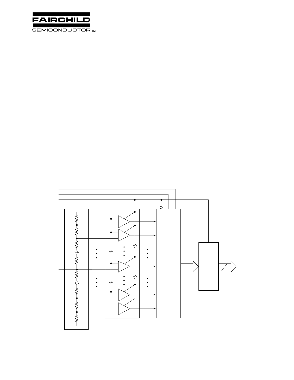
Block Diagram
NMINV
NLINV
CONV
V
IN
R
T
R
1
Description
The TDC1044A is a 25 Msps (Megasample per second) fullparallel analog-to-digital converter, capable of conv erting an
analog signal with full-power frequency components up to
12.5 MHz into 4-bit digital words. Use of a sample-and-hold
circuit is not necessary for operation of the TDC1044A. All
digital inputs and outputs are TTL compatible.
The TDC1044A consists of 15 latching comparators, encoding logic, and an output register. A single convert signal
controls the conversion operation. Output formats are
true/inverted binary or true/in verted of fset two’s complement
codes.
1
R
M
R
B
R
R
R
R
R
R
R/2
REFERENCE
RESISTOR
CHAIN
2
8
14
15
DIFFERENTIAL
COMPARATORS
(15)
15 TO 4
DECODER
LATCH
4
65-1044A-01
D1–D
4
Rev. 1.1.2
Page 2

TDC1044A PRODUCT SPECIFICATION
Functional Description
General Information
The TDC1044A has three functional sections: a comparator
array, encoding logic, and an output re gister . The comparator
array compares the input signal with 15 reference voltages to
produce an N-of-15 thermometer code. All the comparators
referred to voltages more positive than the input signal will
be off, and those referred to voltages more negative than the
input signal will be on. Encoding logic converts the N-of-15
code into binary or two’s complement coding and can invert
either output code. This coding function is controlled by DC
signals on pins NMINV and NLINV. The output register
holds the output constant between updates.
Power
The TDC1044A operates from two power supply voltages,
+5.0V and -5.2V. The return for I
the +5.0V supply) is D
. The return for I
GND
drawn from the -5.2V supply) is A
ground pins must be connected.
Reference
The TDC1044A converts analog signals in the range
V
£
V
RB
IN
applied to R
and V
(the voltage applied to R
RT
ence resistor chain) should be between +0.1V and -1.1V.
V
should be more positive than V
RT
The voltage applied across the reference resistor chain
(V
– V
RT
RB
into digital form. V
£
V
RB
at the bottom of the reference resistor chain)
B
) must be between 0.4V and 1.3V.
(the current drawn from
CC
(the current
EE
. All power and
GND
(the voltage
RB
at the top of the refer-
B
within that range.
RB
Controls
Two function control pins, NMINV and NLINV, set the output format to be either straight binary or offset two’ s complement, in either true or inverted sense, according to Table 1.
These pins are active LOW as signified by the prefix "N" in
the signal name. They may be tied to VCC for a logic "1" and
DGND for a logic "0."
NMINV controls the MSB, D
LSBs: D
, D
and D
2
3
.
4
; NLINV controls the three
1
Convert
The TDC1044A requires a CONVert (CONV) signal. A sample is taken (the comparators are latched) within t
STO
after a
rising edge of CONV. The coded result is translated to the
output latches on the next rising edge. The outputs hold the
previous data a minimum time (t
) after the rising edge of
HO
the CONV signal. New data becomes valid after a maximum
delay time, t
.
D
Analog Input
The TDC1044A uses latching comparators which cause the
input impedance to vary slightly with the signal level. For
optimal performance, the source impedance of the driving
circuit must less than 25 Ohms. Within the range of V
+0.5V, the input signal will not damage the device. If the
input signal is at a voltage between V
RT
and V
RB
will be a binary code between 0 and 15 inclusive. A signal
outside this range will indicate either full-scale positive or
full-scale negative, depending on whether the signal is offscale in the positive or negative direction.
to
EE
, the output
Nominal voltages are V
= 0.00V and V
RT
= -1.00V. These
RB
voltages may be varied dynamically up to 10MHz. Due to
slight variation in the reference currents with clock and input
signals, R
and R
T
should be low-impedance points. For cir-
B
cuits in which the reference is not varied, a bypass capacitor
to ground is recommended. If the reference inputs are varied
dynamically (as in an Automatic Gain Control circuit), a
low-impedance reference source is required.
A reference middle, R
, is also provided; this may be used
M
as an input to adjust the mid-scale point in order to improve
integral linearity . This point may also be used as a tap to supply a mid-scale voltage to offset the analog input. If V
RM
is
used as an output, it must be connected to a high input
impedance device which has small input current. Noise at
this point may adversely affect the performance of this
device.
Outputs
TDC1044A outputs are TTL compatible, and capable of
driving four low-po wer Schottk y TTL (54/74 LS) unit loads.
The outputs hold the previous data a minimum time (t
HO
)
after the rising edge of the CONV signal. Data becomes
valid after a maximum delay time (t
) after the rising edge
D
of CONV. For optimum performance, 2.2 kOhm pull-up
resistors are recommended.
No Connects
Pin 3 of the TDC1044A is labeled No Connect (NC), and has
no connection to the chip. Connect this pin to A
noise performance.
GND
for best
2
Page 3
PRODUCT SPECIFICATION TDC1044A
Table 1. Output Coding
1
Binary Offset Tw o’s Complement
Range
T rue Inverted T rue In verted
-1.00V FS NMINV = 1 0 0 1
NLINV = 1 0 1 0
0.000V 0000 1111 1000 0111
-0.067V 0001 1110 1001 0110
-0.133V 0010 1101 1010 0101
-0.200V 0011 1100 1011 0100
-0.267V 0100 1011 1100 0011
-0.333V 0101 1010 1101 0010
-0.400V 0110 1001 1110 0001
-0.467V 0111 1000 1111 0000
-0.533V 1000 0111 0000 1111
-0.600V 1001 0110 0001 1110
-0.667V 1010 0101 0010 1101
-0.733V 1011 0100 0011 1100
-0.800V 1100 0011 0100 1011
-0.867V 1101 0010 0101 1010
-0.933V 1110 0001 0110 1001
-1.000V 1111 0000 0111 1000
Note:
1. Input voltages are at code centers.
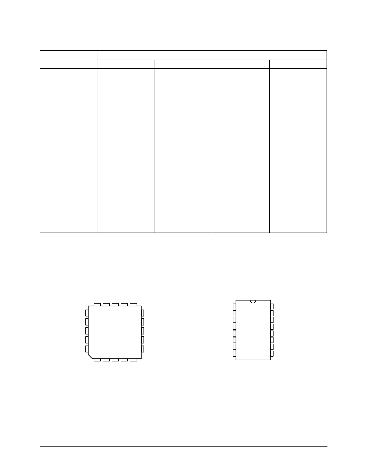
Pin Assignments
(LSB)
4
3D2D1
D
D
18
17
NC
CONV
A
GND
V
NC
19
20
1
2
IN
3
20 Lead PLCC 16 Lead DIP
16
4
5
6
T
R
NC
NC
(MSB)
D
15
14
13
12
11
10
7
8
B
R
V
GND
9
EE
V
CC
NMINV
R
M
NLINV
NC
65-1044A-02
A
GND
V
NC
R
R
V
EE
NLINV
R
1
IN
2
3
T
4
B
5
6
7
8
M
65-1044A-03
CONV
16
D
(LSB)
4
15
D
3
14
D
2
13
D
(MSB)
1
12
D
11
GND
V
10
CC
NMINV
9
3
Page 4
TDC1044A PRODUCT SPECIFICATION
Pin Descriptions
Pin Number
Pin Name
Power
V
CC
V
EE
D
GND
A
GND
Reference
R
T
R
M
R
B
Control
NMINV 9 12 TTL Not MSB Invert
NLINV 7 10 TTL Not LSB Invert
Convert
CONV 16 20 TTL Convert
Analog Input
V
IN
Output
D
1
D
2
D
3
D
4
NC 3 3, 5, 6, 9, 19 A
10 13 +5.0V Positive Supply Voltage
6 8 -5.2V Negative Supply Voltage
11 14 0.0V Digital Ground
1 1 0.0V Analog Ground
4 4 0.0V Reference Resistor, Top
8 11 -0.5V Reference Resistor, Middle
5 7 -1.0V Reference Resistor, Bottom
2 2 0V to -1V Analog Input Signal
12 15 TTL MSB Output
13 16 TTL
14 17 TTL
15 18 TTL LSB Output
Value DescriptionDIP PLCC
GND
No Connect
4
Page 5
PRODUCT SPECIFICATION TDC1044A
C
Absolute Maximum Ratings
(beyond which the device may be damaged)
Type Parameter Min Max Unit
Supply Voltages V
(measured to D
CC
V
(measured to A
EE
A
(measured to D
GND
Input Voltages CONV, NMINV, NLINV (measured to D
V
, V
, V
IN
RT
V
(measured to V
RT
(measured to A
RB
Output Applied voltage (measured to D
Applied current, externally forced
Short circuit duration (single output in high state to ground) 1 sec
Temperature Operating, ambient -55 +125
Operating, junction +150
Lead, soldering (10 seconds) +300
Storage -65 +150
Notes:
1. Absolute maximum ratings are limiting values applied individually while all other parameters are within specified operating
conditions. Functional operation under any of these conditions is NOT implied.
2. Applied voltage must be current limited to specified range.
3. Forcing voltage must be limited to specified range.
4. Current is specified as positive when flowing into the device.
1
) -0.5 7.0 V
GND
) +0.5 -7.0 V
GND
) -0.5 +0.5 V
GND
) -0.5 +5.5 V
GND
) +0.5 V
GND
) -2.2 +2.2 V
RB
2
GND
3,4
)
-0.5 +5.5 V
-1.0 +6.0 mA
EE
V
°
C
°
C
°
C
°
Operating Conditions
Parameter Min. Nom. Max. Units
V
CC
V
EE
V
AGND
t
PWL
t
PWH
V
IL
V
IH
I
OL
I
OH
V
RT
V
RB
VRT – V
V
IN
T
A
Positive Supply Voltage (measured to D
Negative Supply Voltage (measured to A
Analog Ground Voltage (measured to D
CONV Pulse Width, LOW 17 ns
CONV Pulse Width, HIGH 17 ns
Input Voltage, Logic LOW 0.8 V
Input Voltage, Logic HIGH 2.0 V
Output Current, Logic LOW 4.0 mA
Output Current, Logic HIGH -400 mA
Most Positive Reference -1.9 0.0 0.1 V
Most Negative Reference -2.1 -1.0 -0.1 V
Reference Differential 0.2 1.0 2.0 V
RB
Input Voltage V
Ambient Temperature, Still Air 0 70 °C
) 4.75 5.0 5.25 V
GND
) -4.9 -5.2 -5.5 V
GND
) -0.1 0.0 0.1 V
GND
RB
V
RT
V
5
Page 6

TDC1044A PRODUCT SPECIFICATION
Electrical Characteristics
Within specified operating conditions
Parameter Test Conditions Min. Max. Units
I
CC
I
EE
I
REF
R
R
C
I
CB
I
IL
I
IH
I
I
V
V
I
OS
Positive Supply Current VCC = Max, static
Negative Supply Current VEE = Max, static
Reference Current VRT, VRB = Nom 2 mA
Total Reference Resistance 500 Ohms
REF
Input Equivalent Resistance VRT, VRB = Nom, VIN = V
IN
Input Capacitance 25 pF
IN
Input Constant Bias Current VEE = Max 40 mA
Input Current, Logic LOW VCC = Max, VI - 0.5V
Input Current, Logic HIGH VCC = Max, VI = 2.4V 200 mA
Input Current, Max Input Voltage VCC = Max, VI = 5.5V 1.0 mA
Output Voltage, Logic LOW VCC = Min, IOL = Max 0.5 V
OL
Output Voltage, Logic HIGH VCC = Min, IOH = Max 2.4 V
OH
Short Circuit Output Current VCC = Max, One pin to ground, one
C
Note:
1. Worst case: all digital inputs and outputs LOW.
Digital Input Capacitance TA = 25°C, F = 1 MHz 15 pF
I
TA = 0°C to 70°C -50 mA
TA = 70°C -40 mA
CONV -0.8 mA
NMINV, NLINV -0.8 mA
second duration, Output HIGH
1
RB
250 Kohms
15 mA
-300 mA
Switching Characteristics
Within specified operating conditions
Parameter Test Conditions Min. Max. Units
F
t
STO
t
D
t
HO
Maximum Conversion Rate VCC = Min, VEE = Min 25 Msps
S
Sampling Time Offset VCC = Min, VEE = Min 10 ns
Digital Output Delay VCC = Min, VEE = Min, Load 1 30 ns
Digital Output Hold Time VCC = Max, VEE = Max, Load 1 5 ns
6
Page 7

PRODUCT SPECIFICATION TDC1044A
System Performance Characteristics
Within specified operating conditions
Parameter Test Conditions Min. Max. Units
E
LI
E
LD
Linearity Error Integral Independent VRB = Nom 1.6 %
Linearity Error Differential 1.6 %
CS Code Size VRT, VRB = Nom 75 125 % Nominal
E
OT
E
OB
T
CO
Offset Error Top VIN = V
Offset Error Bottom VIN = V
RT
RB
+30 mV
+40 mV
Offset Error Temperature Coefficient ±20 mV/°C
BW Bandwidth, Full Power Input 12.5 MHz
t
E
TR
AP
Transient Response, Full Scale 10 ns
Aperture Error 30 ps
Timing Diagram
CONV
ANALOG
INPUT
DIGITAL
OUTPUT
SAMPLE
N
1
F
S
t
PWH
SAMPLE
N + 1
t
PWL
SAMPLE
N + 2
t
STO
DATA
N – 1
t
HO
t
D
DATA
N
DATA
N + 1
65-1044A-04
7
Page 8

TDC1044A PRODUCT SPECIFICATION
Equivalent Circuits
V
IN
C
V
IN
REFERENCE
RESISTOR
V
EE
CHAIN
V
EE
1-OF-15
COMPARATORS
IN
V
EEA
I
CB
Figure 1. Simplified Analog Input Equivalent Circuit
V
RB
R
IN
65-1044A-05
40pF
+V
CC
810½
1N3062
V
CC
TO
OUTPUT
PIN
V
CC
10K20K
OUTPUT
INPUT
OUTPUT
65-1044A-06
EQUIVALENT
CIRCUIT
Figure 2. Digital Input Equivalent Circuit Figure 3. Output Circuits
LOAD 1
TEST LOAD FOR DELAY
MEASUREMENTS
65-1044A-07
8
Page 9

PRODUCT SPECIFICATION TDC1044A
Applications Discussion
Calibration
To calibrate the TDC1044A, adjust VRT and VRB to set the
1st and 15th thresholds to the desired voltages. Assuming a
0V to -1V desired range, continuously strobe the converter
with -0.0033V (1/2 LSB from 0.000V) on the analog input,
and adjust VRT for output toggling between codes 0000 and
0001. Then apply -0.976V (1/2 LSB from -1.000V) and
adjust VRB for toggling between codes 1110 and 1111.
Instead of adjusting V
ground and the 0V end of the range calibrated with an amplifier offset control. RB is a convenient point for gain adjustment that is not in the analog signal path.
Typical Interface Circuit
The TDC1044A does not require a special input buffer
amplifier to drive the analog input because of its low input
capacitance. A terminated low-impedance transmission line
(<100 Ohms) connected to the VIN terminal of the device is
sufficient if the input voltage levels match those of the A/D
converter.
However, many driver circuits lack sufficient offset control,
drive current, or gain stability. The typical interface circuit in
Figure 4 shows a simple amplifier and voltage reference circuit that may be used with the device. U2 is a wide-band
operational amplifier with a gain factor of -1. As the video
, RT can be connected to analog
RT
input increases from zero to one volt, VIN of the TDC1044A
decreases from zero to -1 volt. With true binary selected
(NMINV = 1 and NLINV = 1), output codes increase from
0000 to 1111.
A small value resistor, R12, serves to isolate the small input
capacitance of the A/D converter from the amplifier output
and insure frequency stability. Pulse and frequency response
of the amplifier are optimized by variable capacitor C12. The
reference voltage for the TDC1044A is generated by amplifier U3. System gain is adjusted by varying R9, which controls the reference voltage level to the A/D converter.
Input voltage range and input impedance for the circuit are
determined by resistors R1 and R2. Formulas for calculating
values for these input resistors are:
1
---------------------------------- -=
R1
and
R2 Z
where VR is the input voltage range of the circuit, ZIN is the
input impedance of the circuit, and the constant 1000 comes
from the value of R3. As shown, the circuit is set up for
1Vp-p 75 Ohm video input.
2VR
æö
----------- -
èø
Z
IN
IN
1
----------- -–
1000
1000 R1
æö
-------------------------
–=
èø
1000 R1+
9
Page 10

TDC1044A PRODUCT SPECIFICATION
+5V
R5
220
R1
R9
2K
10-TURN
"GAIN"
37.4
R2
39.2
R7
1K
R8
2K
10-TURN
"OFFSET"
2
3
–
U3
LM741C
+
VIDEO INPUT
1Vp-p
U4
+
C3
LM313
10
24V
C7
0.1
50V
CLK
–5.2V
R3
1K
R6
2K
C8
0.1
50V
R11
10K
C5
0.1
7
50V
6
C6
4
0.1
50V
14
1
10
–
U2
HA-2539
+
3
L1
FERRITE BEAD
INDUCTOR
C12 1–6pF
R4 2K
C9
0.1
50V
8
C10
0.1
50V
L2
FERRITE BEAD
INDUCTOR
C4
10
25V
R12
27
C11
0.1
50V
D
C1
10
25V
GND
A
+
GND
11
16
3
NC
2
V
IN
1
A
GND
4
R
T
8
R
M
5
R
B
TDC1044A
D
GND
CONV
10
V
CC
D0 (MSB)
D
(LSB)
3
U1
NLINV
NMINV
V
EE
4
D
D
1
2
+
C2
10
25V
R13
2.2K
12
R14
2.2K
13
R15
2.2K
14
R16
2.2K
15
7
9
65-1044A-08
Figure 4. Typical Interface Circuit
10
Page 11

PRODUCT SPECIFICATION TDC1044A
Notes:
11
Page 12

TDC1044A PRODUCT SPECIFICATION
Notes:
12
Page 13

PRODUCT SPECIFICATION TDC1044A
Mechanical Dimensions
16-Lead Ceramic DIP Package
Symbol
A — .200 — 5.08
b1 .014 .023 .36 .58
b2 .050 1.27
c1 .008 .015 .20 .38
D .745 .840 18.92 21.33
E .220 .310 5.59 7.87
e
eA
L .115 .160 2.92 4.06
Q
s1
a
E
s1
Inches
Min. Max. Min. Max.
.065 1.65
.100 BSC 2.54 BSC
.300 BSC 7.62 BSC
.015 .060 .38 1.52
.005 — .13 —
90¡ 105¡ 90¡ 105¡
8
9
Millimeters
D
1
16
Notes
8
2
8
4
4
5, 9
7
3
6
NOTE 1
Notes:
1.
Index area: a notch or a pin one identification mark shall be located
adjacent to pin one. The manufacturer's identification shall not be
used as pin one identification mark.
2.
The minimum limit for dimension "b2" may be .023 (.58mm) for leads
number 1, 8, 9 and 16 only.
3.
Dimension "Q" shall be measured from the seating plane to the base
plane.
4.
This dimension allows for off-center lid, meniscus and glass overrun.
5.
The basic pin spacing is .100 (2.54mm) between centerlines. Each
pin centerline shall be located within ±.010 (.25mm) of its exact
longitudinal position relative to pins 1 and 16.
6.
Applies to all four corners (leads number 1, 8, 9, and 16).
7.
"eA" shall be measured at the center of the lead bends or at the
centerline of the leads when "a" is 90¡.
8.
All leads – Increase maximum limit by .003 (.08mm) measured at the
center of the flat, when lead finish applied.
9.
Fourteen spaces.
e
A
Q
L
b1
eA
a
c1
13
Page 14

TDC1044A PRODUCT SPECIFICATION
Mechanical Dimensions (continued)
16-Lead Plastic DIP Package
Symbol
A — .210 — 5.33
A1 .015 — .38 —
A2 .115 2.93
B .014 .36
B1 .045 .070 1.14 1.78
C .008 .015 .20 .38
D .745 .840 18.92 21.33
D1 .005 — .13 —
E
E1
e
eB — .430 — 10.92
L
N
E1
Inches
Min. Max. Min. Max.
.195 4.95
.022 .56
.300 .325 7.62 8.26
.240 .280 6.10 7.11
.100 BSC 2.54 BSC
.115 .160 2.92 4.06
16 16 5
D
8
Millimeters
1
Notes
4
2
2
Notes:
1.
Dimensioning and tolerancing per ANSI Y14.5M-1982.
2.
"D" and "E1" do not include mold flashing. Mold flash or protrusions
shall not exceed .010 inch (0.25mm).
3.
Terminal numbers are shown for reference only.
4.
"C" dimension does not include solder finish thickness.
5.
Symbol "N" is the maximum number of terminals.
9
D1
e
A
A1
B1
16
E
A2
C
L
B
eB
14
Page 15

PRODUCT SPECIFICATION TDC1044A
Mechanical Dimensions (continued)
20-Lead PLCC Package
Symbol
A .165 .180 4.19 4.57
A1 .090 .120 2.29 3.05
A2 .020 .51——
B .013 .021 .33 .53
B1 .026 .032 .66 .81
D/E .385 .395 9.78 10.03
D1/E1 .350 .356 8.89 9.04
D3/E3 .200 BSC 5.08 BSC
e .050 BSC 1.27 BSC
J .042 .048 1.07 1.22 2
ND/NE 5 5
N20 20
ccc .004 0.10——
Inches
Min. Max. Min. Max.
D
D1
Millimeters
E
E1
Notes
3
J
Notes:
1.
All dimensions and tolerances conform to ANSI Y14.5M-1982
2.
Corner and edge chamfer (J) = 45¡
3.
Dimension D1 and E1 do not include mold protrusion. Allowable
protrusion is .245" (.101mm)
D3/E3
e
A
A1
A2
B1
B
J
– C –
LEAD COPLANARITY
ccc C
15
Page 16

TDC1044A PRODUCT SPECIFICATION
Ordering Information
Product Number Temperature Range Screening Package Package Marking
TDC1044AB9C 0°C to 70°C Commercial 16-Lead Ceramic DIP 1044AB9C
TDC1044AN9C 0°C to 70°C Commercial 16-Lead Plastic DIP 1044AN9C
TDC1044AR4C 0°C to 70°C Commercial 20-Lead PLCC 1044AR4C
LIFE SUPPORT POLICY
FAIRCHILD’S PRODUCTS ARE NOT AUTHORIZED FOR USE AS CRITICAL COMPONENTS IN LIFE SUPPORT DEVICES
OR SYSTEMS WITHOUT THE EXPRESS WRITTEN APPROVAL OF THE PRESIDENT OF FAIRCHILD SEMICONDUCTOR
CORPORATION. As used herein:
1.Life support devices or systems are devices or systems
which, (a) are intended for surgical implant into the body,
or (b) support or sustain life, and (c) whose failure to
perform when properly used in accordance with
instructions for use provided in the labeling, can be
reasonably expected to result in a significant injury of the
user.
2.A critical component in any component of a life support
device or system whose failure to perform can be
reasonably expected to cause the failure of the life support
device or system, or to affect its safety or effectiveness.
www.fairchildsemi.com
5/20/98 0.0m 001
Ó 1998 Fairchild Semiconductor Corporation
Stock#DS7001044A
 Loading...