

Page 1
DATA SH EET
Preliminary specification
File under Integrated Circuits, IC02
July 1994
INTEGRATED CIRCUITS
TDA9860
Universal HiFi audio processor for
TV
Page 2
July 1994 2
Philips Semiconductors Preliminary specification
Universal HiFi audio processor for TV TDA9860
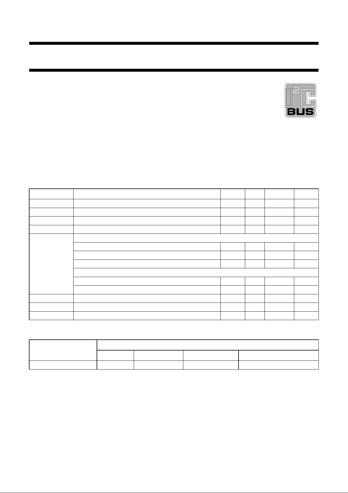
FEATURES
• Multi-source selector switches six AF inputs (three
stereo sources or six mono sources)
• Each of the input signals can be switched to each of the
outputs (crossbar switch)
• Outputs for loudspeaker channel, headphone channel
and peri-TV connector (SCART)
• Switchable spatial stereo and pseudo stereo effects
• Audio surround decoder can be added externally
• Two general purpose logic output ports
• I2C-bus control of all functions.
GENERAL DESCRIPTION
The TDA9860 provides control facilities for the main, the
headphone and the SCART channel of a TV set. Due to
extended switching possibilities, signals from 3 stereo
sources can be handled.
QUICK REFERENCE DATA
ORDERING INFORMATION
Note
1. SOT232-1; 1996 November 21.
SYMBOL PARAMETER MIN. TYP. MAX. UNIT
V
P
positive supply voltage (pin 6) 7.2 8.0 8.8 V
I
P
supply current − 25 − mA
V
i
input signal levels for 0 dB gain (RMS value) 2 −− V
V
o
output signal levels for 0 dB gain (RMS value) 2 −− V
G
v
gain in main channel
volume control (1 dB steps, balance included) −63 − +15 dB
bass control (1.5 dB steps) −12 − +15 dB
treble control (3 dB steps) −12 − +12 dB
gain in headphone channel
volume control (2 dB steps) −70 − 0dB
gain for muting in all channels −80 −− dB
THD total harmonic distortion − 0.1 − %
S/N signal-to-noise ratio − 85 − dB
T
amb
operating ambient temperature 0 − +70 °C
EXTENDED
TYPE NUMBER
PACKAGE
PINS PIN POSITION MATERIAL CODE
TDA9860 32 SDIL plastic SOT232
(1)
Page 3
July 1994 3
Philips Semiconductors Preliminary specification
Universal HiFi audio processor for TV TDA9860
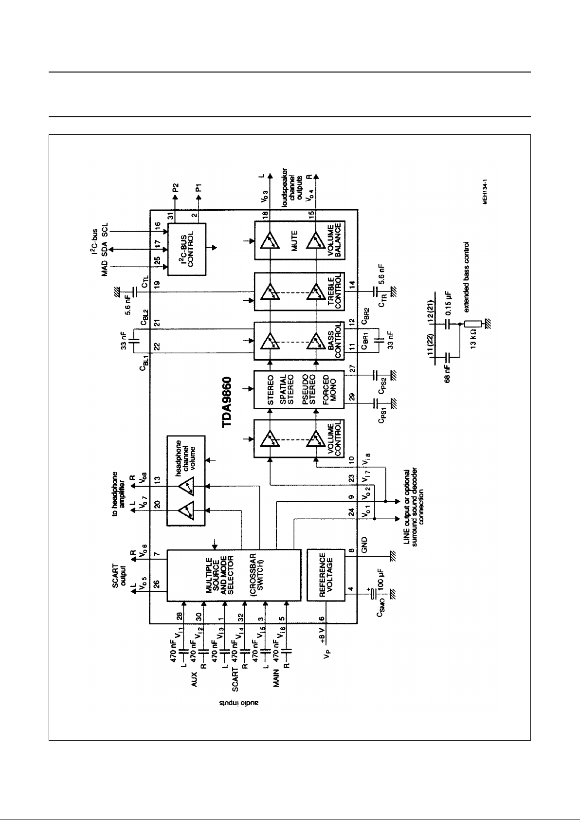
Fig.1 Block diagram and application circuit.
Page 4
July 1994 4
Philips Semiconductors Preliminary specification
Universal HiFi audio processor for TV TDA9860
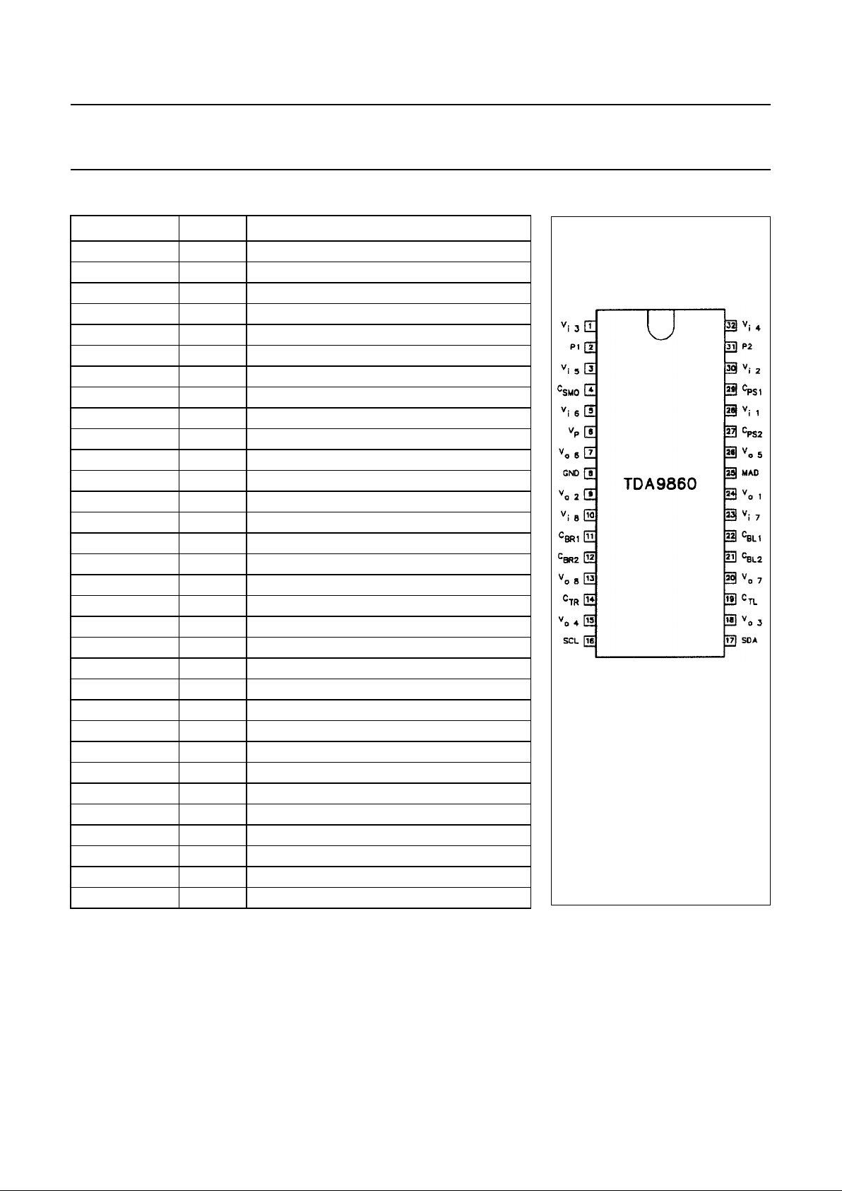
PINNING
SYMBOL PIN DESCRIPTION
V
i 3
1 SCART input signal LEFT
P1 2 port 1 output
V
i 5
3 MAIN input signal LEFT
C
SMO
4 smoothing capacitor of reference voltage
V
i 6
5 MAIN input signal RIGHT
V
P
6 positive supply voltage
V
o 6
7 SCART output signal RIGHT
GND 8 ground
V
o 2
9 MAIN output signal RIGHT
V
i 8
10 input signal RIGHT to loudspeaker channel
C
BR1
11 bass capacitor RIGHT 1
C
BR2
12 bass capacitor RIGHT 2
V
o 8
13 headphone output signal RIGHT
C
TR
14 treble capacitor RIGHT
V
o 4
15 loudspeaker channel output signal RIGHT
SCL 16 I
2
C-bus clock line
SDA 17 I
2
C-bus data line
V
o 3
18 loudspeaker channel output signal LEFT
C
TL
19 treble capacitor LEFT
V
o 7
20 headphone output signal LEFT
C
BL2
21 bass capacitor LEFT 2
C
BL1
22 bass capacitor LEFT 1
V
i 7
23 input signal LEFT to loudspeaker channel
V
o1
24 MAIN output signal LEFT
MAD 25 module address select input
V
o 5
26 SCART output signal LEFT
C
PS2
27 pseudo stereo capacitor 2
V
i 1
28 AUX input signal LEFT
C
PS1
29 pseudo stereo capacitor 1
V
i 2
30 AUX input signal RIGHT
P2 31 port 2 output
V
i 4
32 SCART input signal RIGHT
Fig.2 Pin configuration.
Page 5
July 1994 5
Philips Semiconductors Preliminary specification
Universal HiFi audio processor for TV TDA9860
FUNCTIONAL DESCRIPTION
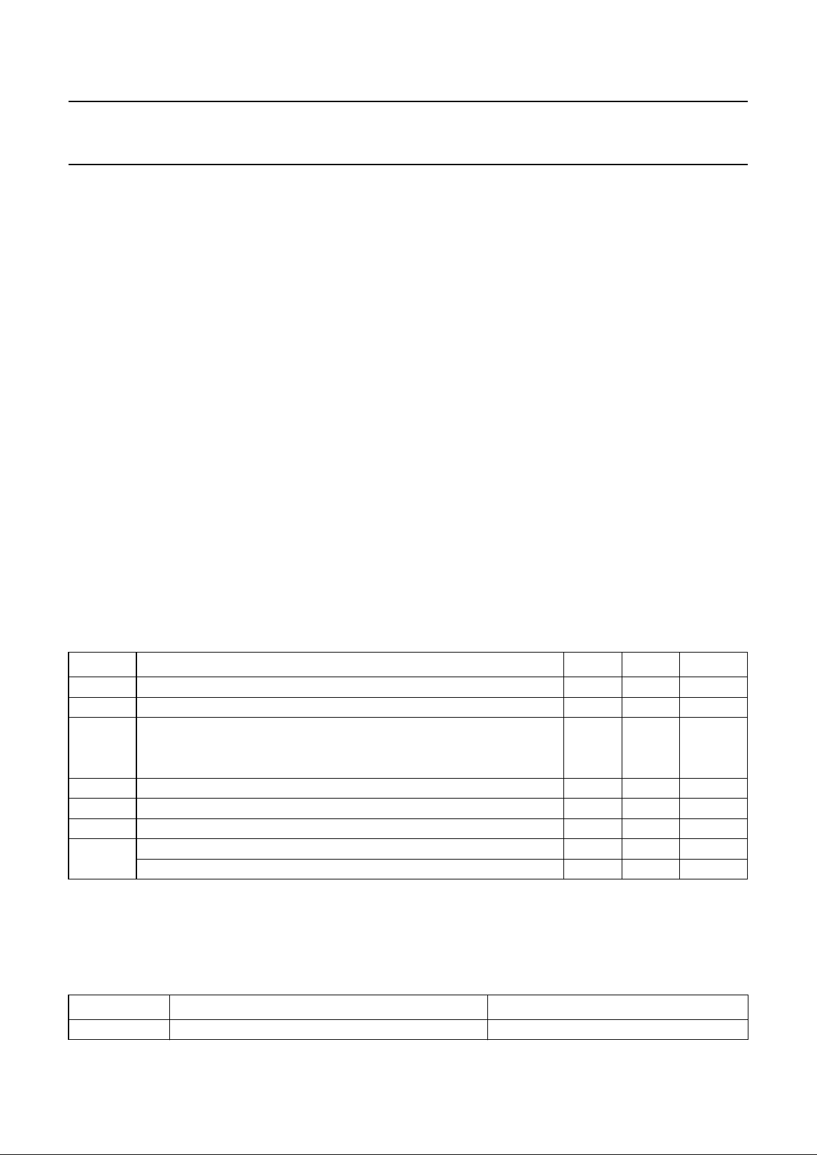
The TDA9860 consists of the following functions:
• source select switching block
• loudspeaker channel with effect controls
• headphone channel
• two port outputs for general purpose
• I2C-bus control
Source select switching block
The TDA9860 selects and switches the input signals from
three stereo or six mono sources as there are MAIN, AUX
and SCART (Fig.1) to one of the outputs SCART,
loudspeaker and headphone (crossbar-switching Table 3).
Due to the fact, that the main channel (LINE outputs) is
looped outside the circuit (from pins 9 and 24 to pins 10
and 23), signals can be used as LINE output or to insert a
‘surround sound decoder’.
Loudspeaker channel
Volume control is divided into the parts volume 1 and
volume 2 / balance. The first part (55 dB) controls left and
right channels simultaneously; the second part (23 dB)
controls volume and balance of left and right channels
independently. Treble control provides a control range
from −12 to +12 dB and bass control from −12 to +15 dB.
Extended bass control can be provided by an external
T-network (Fig.1) from −15 to +19 dB (2 dB steps).
Effect controls
‘Linear stereo’, ‘stereo with spatial effect (30% or 52%
anti-phase crosstalk)’ and ‘forced mono with or without
pseudo-stereo effect’ are controlled by three bits. A muting
of 85 dB is provided.
Headphone channel
The headphone channel is only equipped with volume /
balance control. A muting of 85 dB is provided.
I
2
C-bus control
All settings of control are stored in subaddress registers.
Data transmission is simplified by auto-incrementing the
subaddresses. The on-chip power on reset sets the mute
bit to active, so all 3 stereo outputs are muted.
The muting can be switched off by writing a ‘0’ (non-muted)
into the mute control bits.
LIMITING VALUES
In accordance with the Absolute Maximum Rating System (IEC 134).
Notes to the Limiting Values
1. Equivalent to discharging a 200 pF capacitor through a 0 Ω series resistor.
2. Equivalent to discharging a 100 pF capacitor through a 1.5 kΩ series resistor.
THERMAL RESISTANCE
SYMBOL PARAMETER MIN. MAX. UNIT
V
P
supply voltage (pin 6) 0 10 V
V
n
voltage on all pins, ground excluded 0 V
P
V
I
O
output current
at pins 15, 18, 13, 20, 7 and 26 − 2.5 mA
at pins 2 and 31 − 1.5 mA
P
tot
total power dissipation − 850 mW
T
stg
storage temperature −25 +150 °C
T
amb
operating ambient temperature 0 +70 °C
V
ESD
electrostatic handling for all pins (note 1) −±300 V
electrostatic handling for all pins (note 2) −±2000 V
SYMBOL PARAMETER THERMAL RESISTANCE
R
th j-a
from junction to ambient in free air 60 K/W
Page 6
July 1994 6
Philips Semiconductors Preliminary specification
Universal HiFi audio processor for TV TDA9860
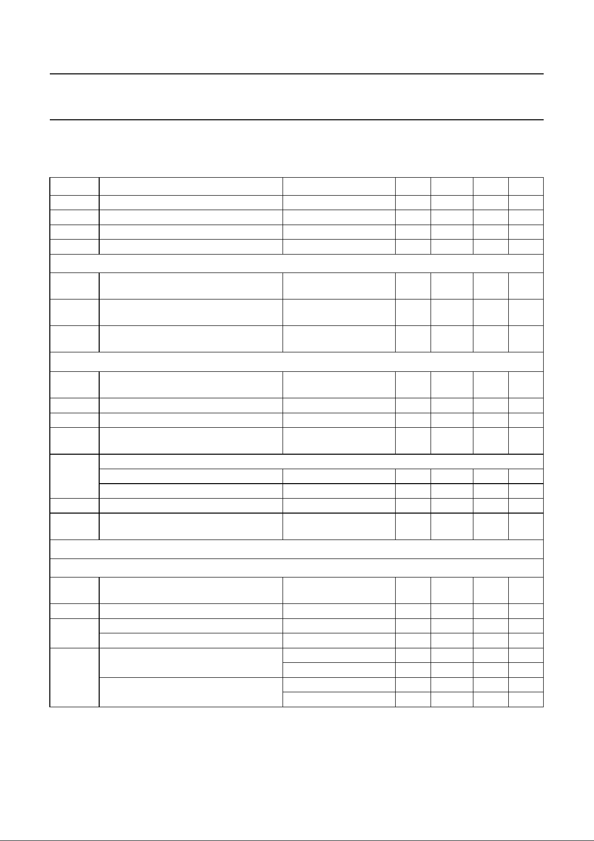
CHARACTERISTICS
V
P
= 8 V; T
amb
= +25 °C; treble and bass in linear positions; balance in mid position; spatial function, pseudo-stereo
function and forced-mono function in off position and measurements taken in Fig.1 unless otherwise specified.
SYMBOL PARAMETER CONDITIONS MIN. TYP. MAX. UNIT
V
P
supply voltage (pin 6) 7.2 8.0 8.8 V
I
P
supply current (pin 6) − 25 − mA
V
ref
internal reference voltage − VP/2 − V
V
4
voltage (pin 4) − VP− 0.1 − V
DC voltage on pins
V
l
DC input voltage (pins 1, 3, 5, 10, 23,
28, 30 and 32)
− VP/2 − V
V
O
DC output voltage (pins 7, 9, 13, 15, 18,
20, 24 and 26)
− VP/2 − V
V
C
DC voltage on capacitors (pins 11, 12,
14, 19, 21, 22, 27 and 29)
− VP/2 − V
Audio select switch. Line, SCART and headphone outputs (controlled via I
2
C-bus, Table 3)
V
i
maximum AF input signal on pins 1, 3,
5, 28, 30, 32 (RMS value)
THD ≤ 0.5%
on output pins
2 −−V
R
i
input resistance (pins 1, 3, 5, 28, 30, 32) 20 30 40 kΩ
f frequency response for all AF outputs −0.5 dB 20 − 20000 Hz
V
o
maximum AF output signal on pins 7, 9,
24, 26 (RMS value)
THD ≤ 0.5% 2 −−V
R
L
allowed external load resistance
on output (pins 9 and 24) 10 −−kΩ
on output (pins 7 and 26) 5 −−kΩ
G
v
gain for all signal arms − 0 − dB
α
cr
switch crosstalk on outputs between
AF inputs at f = 10 kHz
unused inputs
connected to ground
− 90 − dB
LOUDSPEAKER CHANNEL (controlled via I
2
C-bus, Table 3)
Volume control 1 (LEFT and RIGHT simultaneously)
f = 1 kHz, 55 steps
V
i
maximum input signal
(RMS value; pins 10 and 23)
Gv= 0; THD ≤ 0.5% on
output pins 15 and 18
2 −−V
R
i
input resistance (pins 10 and 23) 7.5 10 − kΩ
G
v
nominal volume control −40 − +15 dB
minimum volume control −38 − +14 dB
∆G
v
step width Gv= −32 to +15 dB 0.5 1.0 1.5 dB
G
v
= −40 to −33 dB 0.25 1.0 1.75 dB
gain set error G
v
= −32 to +15 dB −− 1dB
G
v
=−40 to −33 dB −− 2dB
Page 7

July 1994 7
Philips Semiconductors Preliminary specification
Universal HiFi audio processor for TV TDA9860
Volume 2 / balance control
f = 1 kHz, 24 steps
G
v
nominal volume control −24 − 0dB
minimum volume control −23 −−1dB
gain in mute position −80 −85 − dB
∆G
v
step width 0.5 1.0 1.5 dB
gain tracking error −− 2dB
Bass control
G
v
controllable bass CB= 33 nF
maximum boost f = 40 Hz 14 15 16 dB
maximum attenuation f = 40 Hz 11 12 13 dB
∆G
v
step width 1 1.5 2 dB
G
v
controllable enhanced bass Fig.1
maximum boost f = 60 Hz 18 19 20 dB
maximum attenuation f = 60 Hz 14 15 16 dB
∆G
v
step width 1 2 3 dB
Treble control
G
v
controllable treble
maximum boost f = 15 kHz 11 12 13 dB
maximum attenuation f = 15 kHz 11 12 13 dB
∆G
v
step width (resolution) 2.5 3 3.5 dB
Effect controls
α
spat1
anti-phase crosstalk by spatial effect − 52 − %
α
spat2
− 30 − %
ϕ phase shift by pseudo-stereo − Fig.3 −
Loudspeaker channel outputs (pins 15 and 18)
V
o
maximum output signal
(RMS value; pins 15 and 18)
THD ≤ 0.5%;
RL> 10 kΩ;CL<1.5 nF
2 −−V
∆V
15, 18
maximum DC offset voltage between adjoining step and any step to mute
for volume control G
v
= 0 to +15 dB/mute − 215mV
G
v
=−64 to 0 dB/mute − 0.5 10 mV
for bass control G
v
= 0 to +15 dB/mute − 215mV
G
v
=−12 to 0 dB/mute − 0.5 10 mV
for treble control G
v
= −12 to +12 dB/mute − 0.5 10 mV
R
o
output resistance (pins 15 and 18) −− 100 Ω
R
L
allowed output load resistor 10 −−kΩ
C
L
allowed output load capacitor −− 1.5 nF
SYMBOL PARAMETER CONDITIONS MIN. TYP. MAX. UNIT
Page 8

July 1994 8
Philips Semiconductors Preliminary specification
Universal HiFi audio processor for TV TDA9860
V
N(W)
weighted noise voltage at output
(quasi-peak level)
CCIR468-3
for +15 dB gain − 102 −µV
for 0 dB gain − 32 −µV
for −40 dB gain − 27 −µV
for mute position G
v
= −80 dB − 20 −µV
B AF bandwidth −1 dB − 20 to
20000
− Hz
THD total harmonic distortion f = 20 to 12500 Hz
for V
i
= 0.2 V (RMS value) Gv= −30 to +15 dB − 0.1 0.3 %
for V
i
= 1 V (RMS value) Gv= −30 to 0 dB − 0.1 0.3 %
for V
i
= 2 V (RMS value) Gv= −30 to −6 dB − 0.1 0.3 %
α
sp
stereo channel separation f = 10 kHz; Gv= 0 dB;
opposite input grounded
by 1 kΩ resistor
− 75 − dB
α
bus
crosstalk of I2C-bus Gv= 0 dB; note 1 − 100 − dB
RR
100
ripple rejection with 100 Hz ripple on V
P
Gv= 0 dB;
VR< 200 mV RMS
− 55 − dB
HEADPHONE CHANNEL (controlled via I
2
C-bus, Table 3)
Volume control headphone channel
f = 1 kHz, 36 steps
G
v
nominal volume control −70 − 0dB
minimum volume control −67 −−1dB
gain in mute position −80 −85 − dB
∆G
v
step width (resolution) Gv= −36 to 0 dB 1.5 2 2.5 dB
G
v
= −70 to −36 dB 1 2 3 dB
gain set error G
v
= −36 to 0 dB −− 1dB
G
v
=−70 to −36 dB −− 3dB
∆V
13, 20
DC offset voltage for adjoining step and
step to mute
Gv= −70 to 0 dB
− 0.5 10 mV
Headphone channel output (pins 13 and 20)
V
o
maximum output signal (RMS value) THD ≤ 0.5%; RL> 10 kΩ;
C
L
< 1.5 nF
2 −−V
R
o
output resistance −− 100 Ω
R
L
allowed output load resistor 10 −−kΩ
C
L
allowed output load capacitor −− 1.5 nF
V
N(W)
weighted noise voltage at output (quasi-peak level) CCIR468-3
for 0 dB gain − 20 −µV
for −16 dB gain − 15 −µV
for mute position G
v
= −80 dB − 12 −µV
SYMBOL PARAMETER CONDITIONS MIN. TYP. MAX. UNIT
Page 9

July 1994 9
Philips Semiconductors Preliminary specification
Universal HiFi audio processor for TV TDA9860
Note to the characteristics
1. α
bus
= 20 log V
bus
/ Vo(V
bus
= spurious bus signal voltage on AF output pin).
B AF bandwidth −1 dB − 20 to
20000
− Hz
THD total harmonic distortion f = 20 to 12500 Hz
for V
i
= 1 V (RMS value) Gv= −40 to 0 dB − 0.08 0.25 %
α
sp
stereo channel separation f = 10 kHz; Gv= 0 dB;
opposite input grounded
by 1 kΩ resistor
− 75 − dB
α
bus
crosstalk of I2C-bus Gv= 0 dB; note 1 − 100 − dB
RR
100
ripple rejection with 100 Hz ripple on V
P
Gv= 0 dB;
VR< 200 mV RMS
− 55 − dB
SCART output (pins 7 and 26)
V
o
maximum output signal (RMS value) THD ≤ 0.5%; RL> 5 kΩ 2 −−V
R
L
admissible output load resistor 5 −−kΩ
Power on reset
V
PONR
increasing supply voltage
start of reset −− 2.5 V
end of reset 5.2 6.0 6.8 V
V
PONR
decreasing supply voltage start of reset 4.4 5.2 6.0 V
I
2
C-bus, SCL and SDA (pins 16 and 17, observe I2C-bus specification)
V
16, 17
input voltage HIGH-level 3 − V
P
V
input voltage LOW-level 0 − 1.5 V
I
16, 17
input current −− ±10 µA
V
ACK
output voltage at acknowledge (pin 17) I17= −3 mA −− 0.4 V
Module address (pin 25)
V
IL
LOW level input voltage 0 − 1.5 V
V
IH
HIGH level input voltage 3 − V
P
V
Port outputs P1 and P2 (open-collector outputs pins 2 and 31)
V
OL
LOW level output voltage I
2, 31
= 1 mA (sink) −− 0.3 V
I
2, 31
port output current sink current −− 1mA
SYMBOL PARAMETER CONDITIONS MIN. TYP. MAX. UNIT
Page 10

July 1994 10
Philips Semiconductors Preliminary specification
Universal HiFi audio processor for TV TDA9860
I2C-BUS FORMAT
This circuit only operates as a slave transmitter.
If more than 1 byte of DATA is transmitted, then auto-increment of the subaddress is performed.
Byte organisation
Table 1 I
2
C-bus transmission.
S SLAVE ADDRESS A SUBADDRESS A DATA P
S = start condition
SLAVE ADDRESS = 1000 0000 (V
25
= LOW) or 1000 0010 (V25= HIGH)
A = acknowledge, generated by the slave or by the master
SUBADDRESS = subaddress byte, see Table 1
DATA = data byte, see Table 1
P = stop condition
FUNCTION SUBADDRESS HEX
DATA
D7 D6 D5 D4 D3 D2 D1 D0
loudspeaker channel
volume control both 0000 0000 00 0 0 V05 V04 V03 V02 V01 V00
volume/balance left 0000 0001 01 0 0 0 VL4 VL3 VL2 VL1 VL0
volume/balance right 0000 0010 02 0 0 0 VR4 VR3 VR2 VR1 VR0
bass control byte 0000 0011 03 0 0 0 BA4 BA3 BA2 BA1 BA0
treble control byte 0000 0100 04 0000TR3TR2TR1TR0
headphone channel
volume control left 0000 0101 05 0 0 VHL5 VHL4 VHL3 VHL2 VHL1 VHL0
volume control right 0000 0110 06 0 0 VHR5 VHR4 VHR3 VHR2 VHR1 VHR0
switching control byte
headphone output 0000 0111 07 0 MU0 0 0 I03 I02 I01 I00
SCART output 0000 1000 08 0 MU1 P1 P2 I13 I12 I11 I10
loudspeaker output 0000 1001 09 EF2 MU2 EF1 ST I23 I22 I21 I20
Page 11

July 1994 11
Philips Semiconductors Preliminary specification
Universal HiFi audio processor for TV TDA9860
Table 2 Bits of data bytes.
Table 3 Output and input selection by subaddress bytes 07, 08 and 09.
Note
1. X = don’t care
FUNCTION OF THE BITS IN TABLE 1 DESCRIPTION
V00 to V05 volume control common for loudspeaker channel
VL0 to VL4 volume control LEFT for loudspeaker channel
VR0 to VR4 volume control RIGHT for loudspeaker channel
BA0 to BA4 bass control for LEFT and RIGHT loudspeaker channel
TR0 to TR3 treble control for LEFT and RIGHT loudspeaker channel
VHL0 to VHL5 volume control LEFT for headphone channel
VHR0 to VHR5 volume control RIGHT for headphone channel
I00 to I03 input selection for headphone channel
I10 to I13 input selection for SCART channel
I20 to I23 input selection for loudspeaker channel
MU0, MU1 and MU2 mute control bits: 0 = non-muted; 1 = muted
EF1, EF2 and ST special mode control bits
P1 and P2 control bits for port P1 (pin 2) and P2 (pin 31):
output levels: 0 = LOW; 1 = HIGH
OUTPUT AND INPUT CONTROL BYTES, MUTE INCLUDED (EFFECTS TABLE 4)
SELECT OUTPUT PINS INPUT GROUP
INPUT
SIGNAL
ADDR DATA BYTE TO SUBADDRESS
Loudspeaker channels
output pin 18 output pin 15 09 EF2 MU2 EF1 ST I23 I22 I21 I20
SCART channels
output pin 26 output pin 7 08 0 MU1 P1 P2 I13 I12 I11 I10
headphone channels
output pin 20 output pin 13 07 0 MU0 0 0 I03 I02 I01 I00
SELECT INPUT SIGNAL
PINS
HEX BITS OF DATA BYTE
28 28 AUX LEFT V
i1
XB X 0 X X1011
30 30 AUX RIGHT V
i2
X9 X 0 X X1001
28 30 AUX STEREO V
I 1
and V
i 2
X7 X 0 X X0111
1 1 SCART LEFT V
i 3
XA X 0 X X1010
32 32 SCART RIGHT V
i 4
X5 X 0 X X0101
1 32 SCART STEREO V
i 3
and V
i 4
X6 X 0 X X0110
3 3 MAIN LEFT V
i5
XC X 0 X X1100
5 5 MAIN RIGHT V
i 6
XD X 0 X X1101
3 5 MAIN STEREO V
i 5
and V
i 6
X8 X 0 X X1000
Page 12

July 1994 12
Philips Semiconductors Preliminary specification
Universal HiFi audio processor for TV TDA9860
Table 4 Effect controls.
SETTING SPECIAL MODES HEX
DATA BYTE TO SUBADDRESS 09
EF2 MU2 EF1 ST I23 I22 I21 I20
stereo with spatial (52%) BX 1011XXXX
stereo with spatial (30%) 3X 0011XXXX
stereo without spatial 1X 0001XXXX
forced mono with pseudo stereo 2X 0010XXXX
forced mono without pseudo stereo 0X 0000XXXX
Table 5 Volume 2 / balance control LEFT.
G
v
DATA
(dB) HEX VL4 VL3 VL2 VL1 VL0
0 1F11111
−1 1E11110
−2 1D11101
−3 1C11100
−4 1B11011
−5 1A11010
−6 1911001
−7 1811000
−8 1710111
−9 1610110
−10 1510101
−11 1410100
−12 1310011
−13 1210010
−14 1110001
−15 1010000
−16 0F01111
−17 0E01110
−18 0D01101
−19 0C01100
−20 0B01011
−21 0A01010
−22 0901001
−23 0801000
mute left 07 0 0 1 1 1
Table 6 Volume 2 / balance control RIGHT.
G
v
DATA
(dB) HEX VR4 VR3 VR2 VR1 VR0
0 1F11111
−1 1E11110
−2 1D11101
−3 1C11100
−4 1B11011
−5 1A11010
−6 1911001
−7 1811000
−8 1710111
−9 1610110
−10 1510101
−11 1410100
−12 1310011
−13 1210010
−14 1110001
−15 1010000
−16 0F01111
−17 0E01110
−18 0D01101
−19 0C01100
−20 0B01011
−21 0A01010
−22 0901001
−23 0801000
mute right 07 00111
Page 13

July 1994 13
Philips Semiconductors Preliminary specification
Universal HiFi audio processor for TV TDA9860
Table 7 Volume 1 to control both channels.
G
v
DATA
(dB) HEX V05 V04 V03 V02 V01 V00
+15 3F111111
+14 3E111110
+13 3D111101
+12 3C111100
+11 3B111011
+10 3A111010
+9 39111001
+8 38111000
+7 37110111
+6 36110110
+5 35110101
+4 34110100
+3 33110011
+2 32110010
+1 31110001
0 30110000
−1 2F101111
−2 2E101110
−3 2D101101
−4 2C101100
−5 2B101011
−6 2A101010
−7 29101001
−8 28101000
−9 27100111
−10 26100110
−11 25100101
−12 24100100
−13 23100011
−14 22100010
−15 21100001
−16 20100000
−17 1F011111
−18 1E011110
−19 1D011101
−20 1C011100
−21 1B011011
−22 1A011010
−23 19011001
−24 18011000
−25 17010111
−26 16010110
−27 15010101
−28 14010100
−29 13010011
−30 12010010
−31 11010001
−32 10010000
−33 0F001111
−34 0E001110
−35 0D001101
−36 0C001100
−37 0B001011
−38 0A001010
−39 09001001
−40 08001000
G
v
DATA
(dB) HEX V05 V04 V03 V02 V01 V00
Page 14

July 1994 14
Philips Semiconductors Preliminary specification
Universal HiFi audio processor for TV TDA9860
Table 8 Bass control LEFT and RIGHT.
G
v
DATA
(dB) HEX BA4 BA3 BA2 BA1 BA0
+15 19 1 1 0 0 1
+13.5 18 1 1 0 0 0
+12 17 1 0 1 1 1
+10.5 16 1 0 1 1 0
+9 15 1 0 1 0 1
+7.5 14 1 0 1 0 0
+6 13 1 0 0 1 1
+4.5 12 1 0 0 1 0
+3 11 10001
+1.5 10 1 0 0 0 0
0 0F 01111
0 0E 01110
−1.5 0D 0 1 1 0 1
−3 0C 01100
−4.5 0B 0 1 0 1 1
−6 0A 01010
−7.5 09 0 1 0 0 1
−9 08 01000
−10.5 07 0 0 1 1 1
−12 06 0 0 1 1 0
Table 9 Treble control LEFT and RIGHT.
G
v
DATA
(dB) HEX 0 TR3 TR2 TR1 TR0
+12 0A01010
+9 0901001
+6 0801000
+3 0700111
0 0600110
−3 0500101
−6 0400100
−9 0300011
−12 0200010
Page 15

July 1994 15
Philips Semiconductors Preliminary specification
Universal HiFi audio processor for TV TDA9860
Table 10 Volume control of headphone LEFT.
G
v
DATA
(dB) HEX VHL5VHL4VHL3VHL2VHL1VHL
0
03F111111
−23E111110
−43D111101
−63C111100
−83B111011
−103A111010
−1239111001
−1438111000
−1637110111
−1836110110
−2035110101
−2234110100
−2433110011
−2632110010
−2831110001
−3030110000
−322F101111
−342E101110
−362D101101
−382C101100
−402B101011
−422A101010
−4429101001
−4628101000
−4827100111
−5026100110
−5225100101
−5424100100
−5623100011
−5822100010
−6021100001
−6220100000
−641F011111
−661E011110
−681D011101
−701C011100
mute
left
1B011011
Table 11 Volume control of headphone RIGHT.
G
v
DATA
(dB) HEX VHR5VHR4VHR3VHR2VHR1VHR
0
0 3F111111
−2 3E111110
−4 3D111101
−6 3C111100
−8 3B111011
−10 3A111010
−12 39111001
−14 38111000
−16 37110111
−18 36110110
−20 35110101
−22 34110100
−24 33110011
−26 32110010
−28 31110001
−30 30110000
−32 2F101111
−34 2E101110
−36 2D101101
−38 2C101100
−40 2B101011
−42 2A101010
−44 29101001
−46 28101000
−48 27100111
−50 26100110
−52 25100101
−54 24100100
−56 23100011
−58 22100010
−60 21100001
−62 20100000
−64 1F011111
−66 1E011110
−68 1D011101
−70 1C011100
mute
right
1B011011
Page 16

July 1994 16
Philips Semiconductors Preliminary specification
Universal HiFi audio processor for TV TDA9860
CURVE
CAPACITANCE AT PIN 29
(nF)
CAPACITANCE AT PIN 27
(nF)
EFFECT
1 15 15 normal
2 47 5.6 intensified
3 68 5.6 more intensified
Fig.3 Pseudo (phase) as a function of frequency.
Page 17

July 1994 17
Philips Semiconductors Preliminary specification
Universal HiFi audio processor for TV TDA9860
PACKAGE OUTLINE
UNIT b
1
cEe M
H
L
REFERENCES
OUTLINE
VERSION
EUROPEAN
PROJECTION
ISSUE DATE
IEC JEDEC EIAJ
mm
DIMENSIONS (mm are the original dimensions)
SOT232-1
92-11-17
95-02-04
b
max.
w
M
E
e
1
1.3
0.8
0.53
0.40
0.32
0.23
29.4
28.5
9.1
8.7
3.2
2.8
0.181.778 10.16
10.7
10.2
12.2
10.5
1.6
4.7 0.51 3.8
M
H
c
(e )
1
M
E
A
L
seating plane
A
1
w M
b
1
e
D
A
2
Z
32
1
17
16
b
E
pin 1 index
0 5 10 mm
scale
Note
1. Plastic or metal protrusions of 0.25 mm maximum per side are not included.
(1) (1)
D
(1)
Z
A
max.
12
A
min.
A
max.
SDIP32: plastic shrink dual in-line package; 32 leads (400 mil)
SOT232-1
Page 18

July 1994 18
Philips Semiconductors Preliminary specification
Universal HiFi audio processor for TV TDA9860
SOLDERING
Introduction
There is no soldering method that is ideal for all IC
packages. Wave soldering is often preferred when
through-hole and surface mounted components are mixed
on one printed-circuit board. However, wave soldering is
not always suitable for surface mounted ICs, or for
printed-circuits with high population densities. In these
situations reflow soldering is often used.
This text gives a very brief insight to a complex technology.
A more in-depth account of soldering ICs can be found in
our
“IC Package Databook”
(order code 9398 652 90011).
Soldering by dipping or by wave
The maximum permissible temperature of the solder is
260 °C; solder at this temperature must not be in contact
with the joint for more than 5 seconds. The total contact
time of successive solder waves must not exceed
5 seconds.
The device may be mounted up to the seating plane, but
the temperature of the plastic body must not exceed the
specified maximum storage temperature (T
stg max
). If the
printed-circuit board has been pre-heated, forced cooling
may be necessary immediately after soldering to keep the
temperature within the permissible limit.
Repairing soldered joints
Apply a low voltage soldering iron (less than 24 V) to the
lead(s) of the package, below the seating plane or not
more than 2 mm above it. If the temperature of the
soldering iron bit is less than 300 °C it may remain in
contact for up to 10 seconds. If the bit temperature is
between 300 and 400 °C, contact may be up to 5 seconds.
DEFINITIONS
LIFE SUPPORT APPLICATIONS
These products are not designed for use in life support appliances, devices, or systems where malfunction of these
products can reasonably be expected to result in personal injury. Philips customers using or selling these products for
use in such applications do so at their own risk and agree to fully indemnify Philips for any damages resulting from such
improper use or sale.
PURCHASE OF PHILIPS I
2
C COMPONENTS
Data sheet status
Objective specification This data sheet contains target or goal specifications for product development.
Preliminary specification This data sheet contains preliminary data; supplementary data may be published later.
Product specification This data sheet contains final product specifications.
Limiting values
Limiting values given are in accordance with the Absolute Maximum Rating System (IEC 134). Stress above one or
more of the limiting values may cause permanent damage to the device. These are stress ratings only and operation
of the device at these or at any other conditions above those given in the Characteristics sections of the specification
is not implied. Exposure to limiting values for extended periods may affect device reliability.
Application information
Where application information is given, it is advisory and does not form part of the specification.
Purchase of Philips I
2
C components conveys a license under the Philips’ I2C patent to use the
components in the I2C system provided the system conforms to the I2C specification defined by
Philips. This specification can be ordered using the code 9398 393 40011.
 Loading...