

Page 1

INTEGRATED CIRCUITS
DATA SH EET
TDA9855
2
I
C-bus controlled BTSC stereo /
SAP decoder and audio processor
Preliminary specification
File under Integrated Circuits, IC02
July 1994
Page 2
Philips Semiconductors Preliminary specification
I2C-bus controlled BTSC stereo / SAP
decoder and audio processor
FEATURES
• Quasi alignment-free BTSC stereo decoder due to auto
adjustment of channel separation via I2C-bus
• High integration level with automatically tuned
integrated filters
• Input level adjustment I2C-bus controlled
• Alignment-free SAP processing
• dbx noise reduction circuit
• Audio processor
– Selector for internal and external signals (line in)
– Automatic volume level control
– Subwoofer or surround output with separate volume
control
– Volume control
– Special loudness characteristic automatically
controlled in combination with volume setting
TDA9855
– Bass and treble control
– Audio signal zero crossing detection between any
volume step switching
• Mute control at audio signal zero crossing
2
• I
C-bus transceiver.
GENERAL DESCRIPTION
The TDA9855 is a bipolar-integrated BTSC stereo / SAP
decoder with hi-fi audio processor (I
application in TV sets.
2
C-bus controlled) for
ORDERING INFORMATION
P ACKAGE
EXTENDED TYPE NUMBER
PINS
TDA9855 52 SHDIL plastic SOT247AH
TDA9855WP 68 PLCC plastic SOT188CG
Note
1. SOT247-1; 1996 December 5.
2. SOT188-2; 1996 December 5.
A license is required for this product. For further information, please contact:
THAT Corporation
Licensing Operations
734 Forest St.
Marlborough, MA 01752
USA
Tel. (508) 229-2500
Fax: (508) 229-2590
THAT Corporation
Tokyo Office
405 Palm House, 1-20-2 Honmachi
Shibuya-ku, Tokyo 151
Japan
Tel: (03) 3378-0915
Fax: (03) 3374-5191
PIN
POSITION
MA TERIAL CODE
(1)
(2)
July 1994 2
Page 3
Philips Semiconductors Preliminary specification
I2C-bus controlled BTSC stereo / SAP
decoder and audio processor
TDA9855
July 1994 3
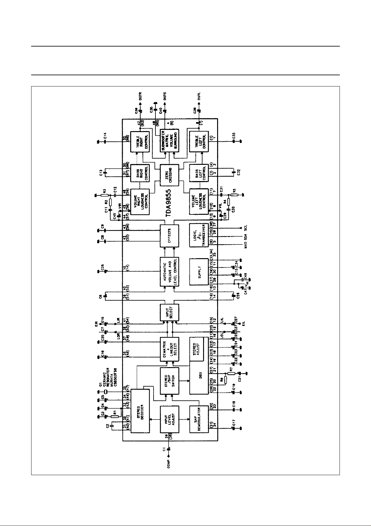
Fig.1 Block, application and test diagram (PLCC pinning in parenthesis).
Page 4
Philips Semiconductors Preliminary specification
I2C-bus controlled BTSC stereo / SAP
decoder and audio processor
COMPONENT LIST
elco ±20%; foil or ceramic ± 10%; resistors ±5% unless otherwise specified.
COMPONENT VALUE TYPE REMARK
C1 10 µF elco 63 V
C2 470 nF foil
C3 4.7 µF elco 63 V
C4 220 nF foil
C5 10 µF elco 63 V; l
C6 2.2 µF elco 16 V
C7 4.7 µF elco 16 V
C8 15 nF foil ±5%
C9 15 nF foil ±5%
C10 2.2 µF elco 63 V
C11 8.2 nF foil or ceramic ±5% SMD 2220/1206
C12 150 nF foil ±5%
C13 33 nF foil ±5%
C14 5.6 nF foil or ceramic ±5% SMD 2220/1206
C15 100 µF elco 16 V
C16 4.7 µF elco 63 V
C17 4.7 µF elco 63 V
C18 100 nF foil
C19 10 µF elco 63 V
C20 4.7 µF elco 63 V
C21 47 nF foil ±5%
C22 1 µF elco 63 V
C23 1 µF elco 63 V
C24 10 µF elco 63 V ± 10%
C25 10 µF elco 63 V ± 10%
C26 2.2 µF elco 16 V
C27 2.2 µF elco 63 V
C28 4.7 µF elco 63 V ± 10%
C29 2.2 µF elco 16 V
C30 8.2 nF foil or ceramic ±5% SMD 2220/1206
C31 150 nF foil ±5%
C32 33 nF foil ±5%
C33 5.6 nF foil or ceramic ±5% SMD 2220/1206
C34 100 µF elco 16 V
C35 150 nF foil ±5%
C36 4.7 µF elco 16 V
C37 4.7 µF elco 16 V
C39 4.7 µF elco 16 V
C40 4.7 µF elco 16 V
leak
< 1.5 µA
TDA9855
July 1994 4
Page 5
Philips Semiconductors Preliminary specification
I2C-bus controlled BTSC stereo / SAP
decoder and audio processor
COMPONENT VALUE TYPE REMARK
C45 2.2 µF elco 16 V
C47 220 µF elco 25 V
C49 100 nF foil or ceramic SMD 1206
COMPONENT VALUE REMARK
R1 2.2 KΩ
R2 20 KΩ
R3 2.2 KΩ
R4 20 KΩ
R5 2.2 KΩ
R6 8.2 KΩ±2%
R7 160 KΩ±2%
Q1 503.5 kHz MURATA CSB503F58
TDA9855
QUICK REFERENCE DATA
SYMBOL PARAMETER CONDITIONS MIN. TYP. MAX. UNIT
V
CC
I
CC
V
comp
V
LOR
G
LA
α
st
THD
V
I, O
, V
L, R
LOL
supply voltage 8.0 8.5 9.0 V
supply current 50 75 95 mA
input signal (RMS value) 100% modulation L + R;
output signal (RMS value) − 500 − mV
f = 300 Hz
− 250 − mV
input level adjustment control range −3.5 −+4.0 dB
stereo channel separation fL= 300 Hz; fR= 3 kHz 25 35 − dB
total harmonic distortion f = 1 kHz − 0.2 − %
signal handling (RMS value) THD < 0.5% 2 −− V
AVL control range −15 −+6dB
G
c
L
B
G
b
G
t
G
v
volume control range −71 −+16 dB
maximum loudness boost f = 40 Hz − 17 − dB
bass control range f = 40 Hz −12 −+16.5 dB
treble control range f = 15 kHz −12 −+12 dB
subwoofer control range f = 40 Hz −14 −+14 dB
S/N signal-to-noise ratio line out (mono);
= 0.5 V (RMS)
V
CCIR noise weighting filter (peak value) − 60 − dB
O
DIN noise weighting filter (RMS value) − 73 − dBA
S/N signal-to-noise ratio audio section;
V
= 2 V (RMS);
CCIR noise weighting filter (peak value) − 94 − dB
DIN noise weighting filter (RMS value) − 107 − dBA
O
gain = 0 dB
July 1994 5
Page 6
Philips Semiconductors Preliminary specification
I2C-bus controlled BTSC stereo / SAP
decoder and audio processor
PINNING
SYMBOL SOT188 SOT247 DESCRIPTION
TL 1 1 treble control capacitor, left channel
n.c. 2 − not connected
B1L 3 2 bass control capacitor, left channel
B2L 4 3 bass control capacitor, left channel
OUTS 5 4 output subwoofer or output surround sound
MAD 6 5 programmable address bit (module address)
OUTL 7 6 output, left channel
n.c. 8 to 10 − not connected
LDL 11 7 input loudness, left channel
VIL 12 8 input volume control, left channel
EOL 13 9 output effects, left channel
CAV 14 10 automatic volume control capacitor
V
REF
LIL 16 12 line input, left channel
n.c. 17 − not connected
AVL 18 13 input automatic volume control, left channel
SOL 19 14 output selector, left channel
LOL 20 15 line output, left channel
TW 21 16 capacitor timing wideband for dbx
TS 22 17 capacitor timing spectral for dbx
CW 23 18 capacitor wideband for dbx
CS 24 19 capacitor spectral for dbx
VEO 25 20 variable emphasis out for dbx
n.c. 26 − not connected
VEI 27 21 variable emphasis in for dbx
n.c. 28 − not connected
CNR 29 22 capacitor noise reduction for dbx
CM 30 23 capacitor mute for SAP
CD 31 24 capacitor DC decoupling for SAP
n.c. 32 − not connected
GND 33 − analog ground
GND 34 − digital ground
GND − 25 common ground
SDA 35 26 serial data input/output
SCL 36 27 serial clock input
V
CC
COMP 38 29 input composite signal
VCAP 39 30 capacitor for electronic filtering of supply
CP1 40 31 capacitor for pilot detector
CP2 41 32 capacitor for pilot detector
15 11 reference voltage 0.5V
37 28 supply voltage
CC
TDA9855
July 1994 6
Page 7
Philips Semiconductors Preliminary specification
I2C-bus controlled BTSC stereo / SAP
decoder and audio processor
SYMBOL SOT188 SOT247 DESCRIPTION
n.c. 42 − not connected
CPH 43 33 capacitor for phase detector
n.c. 44, 45 − not connected
CA 46 34 capacitor for filter adjust
CER 47 35 ceramic resonator
CMO 48 36 capacitor DC decoupling mono
CSS 49 37 capacitor DC decoupling stereo/SAP
LOR 50 38 line output, right channel
SOR 51 39 output selector, right channel
AVR 52 40 input automatic volume control, right channel
n.c. 53 − not connected
LIR 54 41 line input, right channel
PS2 55 42 capacitor 2 pseudo function
PS1 56 43 capacitor 1 pseudo function
EOR 57 44 output effects, right channel
VIR 58 45 input volume control, right channel
LDR 59 46 input loudness, right channel
n.c. 60 to 62 − not connected
OUTR 63 47 output, right channel
n.c. 64 48 not connected
SW 65 49 filter capacitor for subwoofer
B2R 66 50 bass control capacitor, right channel
B1R 67 51 bass control capacitor, right channel
TR 68 52 treble control capacitor
TDA9855
July 1994 7
Page 8
Philips Semiconductors Preliminary specification
I2C-bus controlled BTSC stereo / SAP
decoder and audio processor
TDA9855
Fig.2 Pin configuration for SHRDIL-version.
July 1994 8
Page 9
Philips Semiconductors Preliminary specification
I2C-bus controlled BTSC stereo / SAP
decoder and audio processor
TDA9855
Fig.3 Pin configuration for PLCC-version.
July 1994 9
Page 10

Philips Semiconductors Preliminary specification
I2C-bus controlled BTSC stereo / SAP
decoder and audio processor
FUNCTIONAL DESCRIPTION
Decoder
Input level adjustment
The composite input signal is fed to the input level
adjustment stage. In order to compensate tolerances of
the FM demodulator which supplied the composite input
signal, the TDA9855 provides an input level adjustment
stage. The control range is between −3.5 dB and +4.0 dB
in steps of 0.5 dB. The subaddress control 3 of Tables 2
and 3 and the level adjust setting of Table 16 allows an
optimal signal adjustment during the set alignment in the
production line. This value has to be stored in a none
volatile memory. The maximum input signal voltage is 2 V
(RMS).
Stereo decoder
The output signal of the level adjustment stage is coupled
to a low-pass filter which suppresses the baseband noise
above 125 kHz. The composite signal is then fed into a
pilot detector/pilot cancellation circuit and into the MPX
demodulator. The main L + R signal passes a 75 µs fixed
de-emphasis filter and is fed into the dematrix circuit. The
decoded subsignal L − R is sent to the stereo/SAP switch.
To generate the pilot signal the stereo demodulator uses a
PLL circuit including a ceramic resonator. The stereo
channel separation can be adjusted by an automatic
procedure or manually. A detailed description of this
alignment is provided in the ADJUSTMENT
PROCEDURE. The stereo identification can be read by
2
the I
C-bus (see Table 1). Two different pilot thresholds
can be selected via I2C-bus (see Table 18).
SAP demodulator
The composite signal is fed from the output of the input
level adjustment stage to the SAP demodulator circuit
through a 5f
automatically controlled. The SAP demodulator includes
internal noise and field strength detectors that mute the
SAP output in case of insufficient signal conditions. The
SAP identification signal can be read by the I2C-bus (see
Table 1).
Switch
The stereo/SAP switch feeds either the L − R signal or the
SAP demodulator output signal via the internal dbx noise
reduction circuit to the dematrix/line out select circuit.
Table 15 shows the different switch modes provided at the
output pins LOR and LOL.
band-pass filter. The demodulator level is
H
TDA9855
dbx decoder
The dbx circuit includes all blocks required for the noise
reduction system according to the BTSC system
specification. The output signal is fed through a 73 µs fixed
de-emphasis circuit to the dematrix block.
Integrated filters
The filter functions necessary for stereo and SAP
demodulation and part of the dbx filter circuits are provided
on chip using transconductor circuits. The required filter
accuracy is attained by an automatic filter alignment
circuit.
Audio processor
Selector
The selector allows selecting either the internal line out
signals LOR or LOL (dematrix out) or the external line in
signals LIR and LIL and combines the left and right signals
in several modes (see Table 8). The input signal capability
of the line inputs (LIR/LIL) is 2 V (RMS). The output of the
selector is AC coupled to the automatic volume level
control circuit via pins SOR/SOL and AVR/AVL to avoid
offset voltages.
Automatic volume level control
The automatic volume level stage controls its output
voltage to a constant level of typically 200 mV (RMS) from
an input voltage range between 0.1 and 1.1 V (RMS). The
circuit adjusts variations in modulation during broadcasting
and due to changes in the programme material. The
function can be switched off. To avoid audible ‘plops’
during the permanent operation of the AVL circuit a soft
blending scheme has been applied between the different
gain stages. A capacitor at pin CAV determines the attack
and decay time constants. In addition the ratio of attack
and decay time can be changed via I
and 4 of the CHARACTERISTICS).
Effects
The audio processor section offers the following mode
selections: linear stereo, pseudo stereo, spatial stereo and
forced mono. The spatial mode provides an antiphase
crosstalk of 30% or 52% (switchable via I
Table 13).
Volume/loudness
The volume control range is between +16 dB and −71 dB
in steps of 1 dB and ends with a mute step (see Table 4).
Balance control is achieved by the independent volume
2
C-bus (see notes 3
2
C-bus; see
July 1994 10
Page 11

Philips Semiconductors Preliminary specification
I2C-bus controlled BTSC stereo / SAP
decoder and audio processor
control of each channel. The volume control blocks
operate in combination with the loudness control. The filter
is linear when maximum gain for volume control is
selected. The filter characteristic changes automatically
over a range of 28 dB down to a setting of −12 dB. At
−12 dB volume control the maximum loudness boost is
obtained. The filter characteristic is determined by external
components.
The proposed application provides a maximum boost of
17 dB for bass and 4.5 dB for treble. The loudness may be
switched on or off via the I2C-bus control (see Table 10).
The left and right volume control stages include two
independent zero crossing detectors. In the zero cross
mode a change in volume is automatically activated but
not executed. The execution is enabled at the next zero
crossing of the signal. If a new volume step is activated
before the previous one has been processed, the previous
value will be executed first, and then the new value will be
activated. If no zero crossing occurs the next volume
transmission will enforce the last activated volume setting.
The zero crossing mode is realized between adjoining
steps and between any steps, but not from any step to
mute. In this case the GMU bit is needed to use. In case of
need to mute only one channel, two steps are necessary.
The first step is a transmission from any steps to −71 dB
and the second is −71 dB step to mute. The step of −71 dB
to mute has no zero crossing but it is not relevant. This
procedure has to be provided by software.
Bass control
A single external 33 nF capacitor for each channel in
combination with a linear operational amplifier and internal
resistors provides a bass control range of +16.5 dB to
−12 dB in steps of 1.5 dB at low frequencies (40 Hz).
Internally the basic step width is 3 dB, with intermediate
steps are obtained by a toggle function that provides
additional an 1.5 dB boost or attenuation (see Table 5).
Please note that both loudness and bass control together
result in a maximum bass boost of 34.5 dB for low volume
steps.
Treble control
The adjustable range of the treble control stage is
between −12 dB and +12 B in steps of 3 dB. The filter
characteristic is determined by an external 5.6 nF
capacitor for each channel. The logic circuitry is arranged
in a way that the same data words (HEX 06 to 16) can be
used for both tone controls if a bass control range from
−12 dB to +12 dB and a treble control range from −12 dB
to +12 dB with 3 dB steps are used (see Tables 5 and 6).
TDA9855
Subwoofer;
surround sound control
The subwoofer or the surround mode can be activated with
the control bit SUR (see Table 3). A low bit provides an
output signal (L + R)/2 in subwoofer mode, a high bit
selects surround mode and provides an output signal
(L − R)/2. The signal is fed through a volume control stage
with a range between +14 dB and −14 dB in 2 dB steps on
top of the main channel control to the output pin OUTS.
The last setting is the mute position (see Table 7). The
capacitor C35 at pin SW provides a 230 Hz low-pass filter
in subwoofer mode. In surround mode this capacitor
should be disconnected. If balance is not in mid position
the selected left and right output levels will be combined.
Mute
The mute function can be activated independently with the
last step of volume or subwoofer/surround control at the
left, right or centre output. By setting the general mute bit
GMU via the I
channels include an independent zero cross detector. The
zero crossing mute feature can be selected via bit
TZCM:
TZCM 0:
forced mute with direct execution,
TZCM = 1:
execution in time with signal zero crossing.
In the zero cross mode a change of the GMU bit is
activated but not executed. The execution is enabled at
the next zero crossing of the signal. To avoid a large delay
of mute switching, when very low frequencies are
processed, or the output signal amplitude is lower than the
DC offset voltage, the following I2C-bus transmissions are
needed:
• a first transmission for mute execution
• a second transmission about 100 ms later, which must
switch the zero crossing mode to forced mute
(TZCM = 0)
• a third transmission to reactivate the zero crossing
mode (TZCM = 1). This transmission can take place
immediately, but must follow before the next mute
execution.
2
C-bus all audio part outputs are muted. All
July 1994 11
Page 12
Philips Semiconductors Preliminary specification
I2C-bus controlled BTSC stereo / SAP
TDA9855
decoder and audio processor
LIMITING VALUES
In accordance with the Absolute Maximum Rating System (IEC 134).
SYMBOL PARAMETER CONDITIONS MIN. MAX. UNIT
V
CC
T
amb
T
stg
V
es
V
n
Note to the limiting values
1. Human body model: C = 100 pF; R = 1.5 kΩ; V = 2 kV; charge device model: C = 200 pF; R = 0 Ω; V = 300 V.
THERMAL RESISTANCE
SYMBOL PARAMETER THERMAL RESISTANCE
R
th j-a
supply voltage 0 9.5 V
operating ambient temperature −20 +70 °C
storage temperature −65 +150 °C
electrostatic handling note 1
voltage at all other pins to pin GND 0 V
CC
V
from junction to ambient in free air
SOT247AH 43 K/W
SOT188CG 38 K/W
July 1994 12
Page 13

Philips Semiconductors Preliminary specification
I2C-bus controlled BTSC stereo / SAP
TDA9855
decoder and audio processor
Requirements for the composite input signal to ensure proper system performance.
SYMBOL PARAMETER CONDITIONS MIN. TYP. MAX. UNIT
COMP
composite input level for 100%
L+R
modulation L + R (25 kHz
deviation), RMS, f = 300 Hz
∆COMP composite input level spreading
under operating conditions
Z
O
f
−2 dB
output impedance note 1 − low-ohmic 5 kΩ
roll-off frequencies (25 kHz
deviation L + R)
THD total harmonic distortion L + R;
f = 1 kHz
S/N signal-to-noise ratio
L + R/noise
α
SB
side band suppression mono into
unmodulated SAP carrier;
SAP carrier/side band
α
SP
spectral spurious attenuation
L + R/spurious
measured at COMP 162 250 363 mV
T
= −20 to +70 °C; aging;
amb
−0.5 −+0.5 dB
power supply influence
low frequency (−2 dB) −− 5Hz
high frequency (−2 dB) 100 −−kHz
25 kHz deviation −− 0.5 %
125 kHz deviation; note 2 −− 1.5 %
CCIR 468-2 weighted quasi peak; L + R; 25 kHz deviation;
f = 1 kHz; 75 µs de-emphasis
critical picture modulation 44 −−dB
with sync only 54 −−dB
mono signal: 25 kHz
46 −−dB
deviation,
f = 1 kHz; side band: SAP
carrier frequency ±1 kHz
50 Hz to 100 kHz; mainly
40 −−dB
n x fH; no de-emphasis; L + R:
25 kHz deviation, f = 1 kHz
Notes to the requirements
1. Low-ohmic preferred, otherwise the signal loss and spreading at COMP, caused by ZO and the composite input
impedance (see input level adjustment control) must be taken into account.
2. In order to prevent clipping at overmodulation (maximum deviation in the BTSC system for 100% modulation is
73 kHz).
July 1994 13
Page 14
Philips Semiconductors Preliminary specification
I2C-bus controlled BTSC stereo / SAP
TDA9855
decoder and audio processor
CHARACTERISTICS
All voltages are measured relative to GND; V
AC coupled; f = 1 kHz; T
= +25 °C; volume gain control Gc= 0 dB; bass linear; treble linear; loudness off; AVL off;
amb
effects linear; composite input signal according to BTSC standard; see block diagram unless otherwise specified.
SYMBOL PARAMETER CONDITIONS MIN. TYP. MAX. UNIT
V
CC
I
CC
V
DC
supply voltage 8.0 8.5 9.0 V
supply current 50 75 95 mA
DC voltage at signal
handling pins
DECODER SECTION
Input level adjustment control
G
LA
input level adjustment
control
G
step
V
i(RMS)
Z
i
step resolution − 0.5 − dB
maximum input level 2 −−V
input impedance 29.5 35 40.5 kΩ
Stereo decoder
MPX
L + R
input level for 100%
modulation L + R (25 kHz
deviation) (RMS value)
MPX
L − R
input level for 100%
modulation L − R
(50 kHz deviation)
(peak value)
MPX
MPX
max
pilot
headroom for L + R, L, R f
nominal stereo pilot level
(RMS value)
ST
ON
pilot threshold STEREO
ON (RMS value)
ST
OFF
pilot threshold STEREO
OFF (RMS value)
Hyst hysteresis − 2.5 − dB
Out
L+R
output level for 100%
modulation L + R at LINE
OUT
α
ST
stereo channel
separation L/R at LINE
OUT
= 8.5 V, source resistance≤600Ω, output load RL≥ 10 kΩ, CL≤ 2.5 nf,
CC
− VCC/2 − V
maximum gain − 4.0 − dB
maximum attenuation −−3.5 − dB
input level adjusted via I2C-bus
− 250 − mV
(L + R; f = 300 Hz); monitoring
LINE OUT
− 707 − mV
< 15 kHz; THD < 15% for
mod
9 −−dB
75 µs equivalent input modulation
− 50 − mV
data STS = 1 −− 35 mV
data STS = 0 −− 30 mV
data STS = 1 15 −−mV
data STS = 0 10 −−mV
input level adjusted via I2C-bus
480 500 520 mV
(L + R; f = 300 Hz); monitoring
LINE OUT
aligned with dual tone 14%
modulation; alignment at
fL= 300 Hz; fR= 3.1 kHz
= 300 Hz; fR= 3 kHz 25 35 − dB
f
L
f
= 300 Hz; fR= 8 kHz 20 30 − dB
L
= 300 Hz; fR= 10 kHz 15 25 − dB
f
L
July 1994 14
Page 15
Philips Semiconductors Preliminary specification
I2C-bus controlled BTSC stereo / SAP
TDA9855
decoder and audio processor
SYMBOL PARAMETER CONDITIONS MIN. TYP. MAX. UNIT
L, R
(f)
THD
L,R
S/N S/N CCIR 468-2
Stereo decoder, oscillator (VCXO)
f
o
f
of
Remark: The oscillator is designed to work together with MURATA resonator CSB503F58 for TDA9855. Change of
the resonator supplier is possible, but the resonator specification must be close to CSB503F58 for TDA9855.
∆f
H
L, R frequency response 14% modulation;
f
reference
= 300 Hz L or R
50 Hz to 11 kHz −3 −−dB
12 kHz −−3 −dB
total harmonic distortion
L, R at
modulation L or R 1% to
100%; f = 1 kHz
LINE OUT
LINE OUT in position MONO 50 60 − dB
weighted; quasi peak;
V
= 500 mV (RMS)
O
nominal VCXO frequency
(32fH)
with nominal ceramic
resonator
spread of free running
frequency
capture range (nominal
pilot)
− 0.2 1.0 %
− 503.5 − kHz
500.0 − 507.0 kHz
±190 ±265 − Hz
SAP demodulator
Remark: The internal SAP carrier level is determined by the composite input level and the level adjust gain.
SAP
IN
nominal SAP carrier input
level
15 kHz frequency deviation
of intercarrier
− 150 − mV
(RMS value)
SAP
ON
pilot threshold SAP ON
−− 85 mV
(RMS value)
SAP
OFF
pilot threshold SAP OFF
35 −−mV
(RMS value)
SAP
SAP
HYS
LEV
hysteresis − 2 − dB
SAP output level at LINE
OUT
(RMS value)
LINE OUT (LOL, LOR) in
position SAP / SAP;
f
= 300 Hz;
mod
− 500 − mV
100% modulation
F
res
frequency response 14% modulation; 50 Hz to
8 kHz; f
reference
= 300 Hz
−3 −−dB
THD total harmonic distortion 1 kHz − 0.5 2.0 %
LINE OUT (at pins LOL, LOR)
V
o
nominal output voltage
100% modulation − 500 − mV
(RMS value)
Headr output headroom 9 −−dB
Z
o
Out
R
L
DC
output impedance − 80 120 Ω
DC output voltage 0.45VCC0.5V
output load resistance
5 −−kΩ
CC
0.55VCCV
(AC)
July 1994 15
Page 16

Philips Semiconductors Preliminary specification
I2C-bus controlled BTSC stereo / SAP
TDA9855
decoder and audio processor
SYMBOL PARAMETER CONDITIONS MIN. TYP. MAX. UNIT
C
L
α
ST-SAP
α
SAP-ST
∆V
ST-SAP
dbx noise reduction circuit
t
adj
I
s
∆I
s
I
s range
I
t
Rel
rate
output load capacitance −− 2.5 nF
idle crosstalk L, R into
SAP
100% modulation; f = 1 kHz; L or
R; LINE OUT switched to
50 −−dB
SAP / SAP
idle crosstalk SAP into L,R100% modulation; f = 1 kHz;
50 −−dB
SAP; LINE OUT switched to
stereo
output voltage difference
250 Hz to 6.3 kHz −− 3dB
if
switched from L, R to SAP
stereo adjust time see adjustment procedure −− 1s
nominal timing current for
nominal release rate of
spectral
Is can be measured at pin 17 (pin
22) via current meter connected
to VCC/2 + 1 V
− 24 −µA
RMS detector
spread of timing current −− 15 %
timing current adjustment
7 steps via I2C-bus −±30 − %
range
timing current for release
− Is/3 −µA
rate of
wideband RMS detector
nominal RMS detector
release rate
nominal timing current and
external capacitor values
wideband − 125 − dB/s
spectral − 381 − dB/s
AUDIO PART
Circuit section from pins LIL, LIR to pins OUTL, OUTR, OUTS
Select in to input line control
B roll-off frequencies C
, C7, C10, C26, C27,
6
C29= 2.2 µF; Zi=Z
low frequency (−3 dB) −− 20 Hz
high frequency (−0.5 dB) 20 −−kHz
THD total harmonic distortion V
= 1 V (RMS); Gc= 0 dB;
i
AVL on
= 2 V (RMS); Gc= 0 dB;
V
i
AVL on
V
= 1 V (RMS); Gc= 0 dB;
i
AVL off
V
= 2 V (RMS); Gc= 0 dB;
i
AVL off
RR power supply ripple
V
< 200 mV; f = 100 Hz 47 50 − dB
r(RMS)
rejection
July 1994 16
i min
− 0.2 0.5 %
− 0.2 0.5 %
− 0.05 − %
− 0.02 − %
Page 17

Philips Semiconductors Preliminary specification
I2C-bus controlled BTSC stereo / SAP
TDA9855
decoder and audio processor
SYMBOL PARAMETER CONDITIONS MIN. TYP. MAX. UNIT
α
B
V
no
α
CS
Selector (from pins LOL, LOR, LIL, LIR to pins SOL, SOR)
Z
i
α
s
V
i(RMS)
V
DC OFF
Z
o
R
L
C
L
G
c
Automatic volume level control (AVL)
Z
i
V
i(RMS)
G
v
G
step
V
i(RMS)
V
o(RMS)
crosstalk (20 log
V
bus(p-p)
V
o(RMS)
/
between bus
note 1 − 110 − dB
inputs and
signal outputs
noise output voltage CCIR 468-2 weighted; quasi peak − 40 80 µV
measured in dBA − 8 −µV
channel separation Vi= 1 V; f = 1 kHz 75 −−dB
= 1 V; f = 12.5 kHz 75 −−dB
V
i
input impedance 16 20 24 kΩ
input isolation of one
f = 1 kHz; Vi=1 V 86 96 − dB
selected source to the
other input
f = 12.5 kHz; V
=1 V 80 96 − dB
i
maximum input voltage THD < 0.5% 2 2.3 − V
DC offset voltage at
−− 25 mV
selector out
by selection of any inputs
output impedance − 80 120 Ω
output load resistance
5 −−kΩ
(AC)
output load capacitance −− 2.5 nF
voltage gain, selector − 0 − dB
input impedance 8.8 11.0 13.2 kΩ
maximum input voltage THD < 0.2% 2 −−V
gain, maximum boost 5 6 7 dB
maximum attenuation 14 15 16 dB
equivalent step width
− 1.5 − dB
between the input stages
(soft switching
system)
input level at maximum
see Fig.4 − 0.1 − V
boost
input level at maximum
− 1.125 − V
attenuation
output level in AVL
160 200 250 mV
operation range
July 1994 17
Page 18

Philips Semiconductors Preliminary specification
I2C-bus controlled BTSC stereo / SAP
TDA9855
decoder and audio processor
SYMBOL PARAMETER CONDITIONS MIN. TYP. MAX. UNIT
V
DC OFF
R
att
I
dec
Effect controls
α
spat1
α
spat2
ϕ phase shift by
DC offset between
different gain steps
discharge resistors for
attack time constant
charge current for decay
time
anti-phase crosstalk by
spatial
effect
pseudo-stereo
note 2; voltage at pin CAV
6.50 V to 6.33 V −− 6mV
6.33 V to 6.11 V −− 6mV
6.11 V to 5.33 V −− 6mV
5.33 V to 2.60 V −− 6mV
note 3;
AT1 = 0; AT2 = 0 340 420 520 Ω
AT1 = 1; AT2 = 0 590 730 910 Ω
AT1 = 0; AT2 = 1 0.96 1.2 1.5 kΩ
AT1 = 1; AT2 = 1 1.7 2.1 2.6 kΩ
note 4 1.6 2.0 2.4 µA
− 52 − %
− 30 − %
see Fig.5 −− −−
Volume tone control part (input pins VIL, VIR to pins OUTX, to pin OUTS)
Z
i
input impedance volume
input
Z
o
R
L
output impedance − 80 120 Ω
output load resistance
(AC)
C
L
V
i(RMS)
V
no
output load capacitance −− 2.5 nF
maximum input voltage THD < 0.5% 2.0 2.15 − V
noise output voltage CCIR 468-2 weighted;
quasi peak
G
= 16 dB − 110 220 µV
c
G
= 0 dB − 33 50 µV
c
mute position − 10 −µV
G
c
total continuous control
range
maximum boost − 16 − dB
maximum attenuation − 71 − dB
G
step
step resolution − 1 − dB
step error between any
adjoining step −− 0.5 dB
8.0 10.0 12.0 kΩ
5 −−kΩ
July 1994 18
Page 19

Philips Semiconductors Preliminary specification
I2C-bus controlled BTSC stereo / SAP
TDA9855
decoder and audio processor
SYMBOL PARAMETER CONDITIONS MIN. TYP. MAX. UNIT
∆G
a
∆G
t
α
m
V
DC OFF
Loudness control part
L
B
Bass control (see Fig.7)
G
b
G
step
V
DC OFF
attenuation set error Gc= +16 to −50 dB −− 2dB
G
=−51 to −71 dB −− 3dB
c
gain tracking error Gc= +16 to −50 dB −− 2dB
mute attenuation 80 −−dB
DC step offset between
any adjacent step
DC step offset between
any step to mute
Gc= +16 to 0 dB − 0.2 10.0 mV
G
= 0 to −71 dB −− 5mV
c
= +16 to +1dB − 215mV
G
c
G
= 0 to −71 dB − 110mV
c
maximum loudness boost loudness on; referred to
loudness off; boost is
determined by external
components; see Fig.6;
f = 40 Hz − 17 − dB
f = 10 kHz − 4.5 − dB
bass control maximum
f = 40 Hz 15.5 16.5 17.5 dB
boost
maximum attenuation f = 40 Hz 11 12 13 dB
step resolution f = 40 Hz − 1.5 − dB
step error between any
adjoining step −− 0.5 dB
DC step offset between
−− 15 mV
any
adjacent step
Treble control (see Fig.8)
G
t
treble control maximum
f = 15 kHz 11 12 13 dB
boost
maximum attenuation f = 15 kHz 11 12 13 dB
maximum boost f > 15 kHz −− 15 dB
G
step
step resolution f = 15 kHz − 3 − dB
step error between any
adjoining step
V
DC OFF
DC step offset between
any
adjacent step
Subwoofer or surround control
G
s
subwoofer control f = 40 Hz
maximum boost 12 14 16 dB
maximum attenuation 12 14 16 dB
G
step
step resolution − 2 − dB
July 1994 19
−− 0.5 dB
−− 10 mV
Page 20

Philips Semiconductors Preliminary specification
I2C-bus controlled BTSC stereo / SAP
TDA9855
decoder and audio processor
SYMBOL PARAMETER CONDITIONS MIN. TYP. MAX. UNIT
α
m
V
DC OFF
R
F
L+R
mute attenuation 60 −−dB
DC step offset between
any adjacent step
DC step offset between
any
step to mute
Gs= 0 to +14 dB −− 10 mV
G
= 0 to −14 dB −− 5mV
s
G
= +2 to +14 dB without input
s
−− 15 mV
offset
(pin SW connected to V
G
= +2 to +14 dB inclusive offset
s
REF
)
−− 50 mV
from OUTR, OUTL
G
= 0 to −14 dB −− 10 mV
s
internal resistor for
45 6kΩ
low-pass filter with
external capacitor at
pin SW
common mode rejection
REJ
in
surround sound at pin
mono signal at VIL/VIR;
F = 1 kHz; Vi=1 V;
balance = 0 dB
26 36 − dB
OUTS
Muting at power supply drop for OUTL, OUTR, OUTS
V
CC-DROP
supply drop for mute
− V
− 0.7 − V
CAP
active
Power on reset
When reset is active the GMU-bit (general mute) and the LMU-bit (LINEOUT - mute) is set and the I2C-bus receiver
is in reset position
V
CC
start of reset increasing supply voltage −− 2.5 V
end of reset 5.2 6 6.8 V
start of reset decreasing supply voltage 4.2 5 5.8 V
Digital part (I
V
IH
V
IL
I
IH
I
IL
V
OL
2
C-bus pins; note 5)
HIGH level input voltage 3 − V
CC
V
LOW level input voltage −0.3 −+1.5 V
HIGH level input current −10 −+10 µA
LOW level input current −10 −+10 µA
LOW level output voltage IL= 3 mA −− 0.4 V
July 1994 20
Page 21

Philips Semiconductors Preliminary specification
I2C-bus controlled BTSC stereo / SAP
TDA9855
decoder and audio processor
Notes to the characteristics
1. The transmission contains:
- total initialization with MAD and SAD for volume and 11 DATA words, see also definition of characteristics
- clock frequency = 50 kHz
- repetition burst rate = 400 Hz
- maximum bus signal amplitude = 5 V
2. The listed pin voltage corresponds with typical gain steps of +6 dB, +3 dB, 0 dB, −6 dB, −15 dB.
3. Attack time constant = CAVxR
C
0.76 V 10
×
AV
4. Decay time =
Example: C
-----------------------------------------------------------------------------------
= 4.7 µF; I
AV
dec
.
att
G
–
--------- -
20
I
dec
=2µA; Gv1= −9 dB; Gv2= +6 dB → decay time result: 4.14 s.
5. The AC characteristics are in accordance with the I2C-bus specification. Full specification of I2C-bus will be supplied
on request. The maximum clock frequency is 100 kHz.
.
p-p
v1
G
v2
–
--------- 20
10
–
July 1994 21
Page 22

Philips Semiconductors Preliminary specification
I2C-bus controlled BTSC stereo / SAP
TDA9855
decoder and audio processor
ADJUSTMENT PROCEDURE
Composite input level adjustment. Feed in from FM demodulator the composite signal with 100% modulation (25 kHz
deviation) L + R, f = 300 Hz. Set input level control via I2C-bus monitoring line out (500 mV ± 20 mV). Store the setting
in a none volatile memory. Adjustment of spectral and wideband expander via stereo channel separation adjust.
Automatic adjustment procedure
• Capacitors of external inputs EIL, EIR must be grounded
• Composite input signal L = 300 Hz, R = 3.1 kHz, 14% modulation for each channel; volume gain +16 dB via I
To avoid annoying sound level set GMU bit to ‘1’ during adjustment procedure
• Effects, AVL, loudness off
• Selector setting SC0, SC1, SC2 = 0, 0, 0 (see Table 8)
• Line out setting bits: STEREO = 1, SAP = 0 (see Table 15)
• Start adjustment by transmission ADJ = 1 in register ALI3. The decoder will align itself
• After 1 s, stop alignment by transmitting ADJ = 0 in register ALI3 read the alignment data by an I2C-bus read operation
from ALR1 and ALR2 (see I2C-bus protocol) and store it in a none volatile memory. The alignment procedure
overwrites the previous data stored in ALI1 and ALI2
• Disconnect the capacitors of external inputs from ground.
2
C-bus.
Manual adjust
Manual adjust is necessary when no dual tone generator is available (e.g. for service).
• Spectral and wideband data have to be set to 10000 (middle position for adjustment range)
• Composite input L = 300 Hz, 14% modulation
• Adjust channel separation by varying wideband data
• Composite input L = 3 kHz, 14% modulation
• Adjust channel separation by varying spectral data
• Iterative spectral/wideband operation for optimal adjust
• Store data in none volatile memory.
After every POWER ON, the alignment data and the input level adjustment data must be loaded from the none volatile
memory.
Timing current for release rate
2
Due to possible internal and external spreading, the timing current can be adjusted via I
recommended by dbx.
C-bus, see Table 19, as
July 1994 22
Page 23

Philips Semiconductors Preliminary specification
I2C-bus controlled BTSC stereo / SAP
TDA9855
decoder and audio processor
I2C-BUS PROTOCOL
2
C-bus format to read (slave transmits data)
I
S SLAVE ADDRESS R/W A DATA MA DATA P
Where:
S = start condition, generated by the master
standard SLAVE ADDRESS = 101 101 1 pin MAD not connected
pin programmable SLAVE ADDRESS = 101 101 0 pin MAD connected to ground
R/W = 1 (read), generated by the master
A = acknowledge, generated by the slave
DATA = slave transmits an 8-bit data word
MA = acknowledge, generated by the master
P = stop condition, generated by the master
Table 1 Definition of the transmitted bytes after read condition.
FUNCTION BYTE
Alignment read 1 ALR1 Y SAPP STP A14 A13 A12 A11 A10
Alignment read 2 ALR2 Y SAPP STP A24 A23 A22 A21 A20
Function of the bits:
STP stereo pilot identification (stereo received = 1)
SAPP SAP pilot identification (SAP received = 1)
A1x to A2x stereo alignment read data
A1x for wideband expander
A2x for spectral expander
Y indefinite
MSB
D7 D6 D5 D4 D3 D2 D1
LSB
D0
The master generates an acknowledge when it has received the first data word, ALR1, then the slave transmits the next
data word ALR2. The master next generates an acknowledge, then the slave begins transmitting the first data word
ALR1, and so on until the master generates no acknowledge and transmits condition P.
July 1994 23
Page 24

Philips Semiconductors Preliminary specification
I2C-bus controlled BTSC stereo / SAP
TDA9855
decoder and audio processor
I2C-bus format to write (slave receives data)
S SLAVE ADDRESS R/W A SUBADDRESS A DATA A P
Where:
S = start condition
standard SLAVE ADDRESS = 101 101 1 pin MAD not connected
pin programmable SLAVE ADDRESS = 101 101 0 pin MAD connected to ground
R/W = 0 (write)
A = acknowledge, generated by the slave
SUBADDRESS (SAD) = see Table 2
DATA = see Table 3
P = stop condition
If more than 1 byte of DATA is transmitted, then auto-increment is performed, starting from the transmitted subaddress
and auto-increment of subaddress according to the order of Table 2 is performed.
Subaddress
Table 2 Second byte after slave address.
FUNCTION REGISTER
volume right VR 0 0 0 0 000000
volume left VL 0 0 0 0 000101
bass BA 0 0 0 0 001002
treble TR 0 0 0 0 001103
subwoofer SW 0 0 0 0 010004
control 1 CON1 0 0 0 0 010105
control 2 CON2 0 0 0 0 011006
control 3 CON3 0 0 0 0 011107
alignment 1 ALI1 0 0 0 0 100008
alignment 2 ALI2 0 0 0 0 100109
alignment 3 ALI3 0 0 0 0 10100A
MSB
D7 D6 D5 D4 D3 D2 D1
LSB
D0
HEX
July 1994 24
Page 25

Philips Semiconductors Preliminary specification
I2C-bus controlled BTSC stereo / SAP
TDA9855
decoder and audio processor
Definition of third byte
Table 3 Third byte after slave address.
FUNCTION REGISTER
volume right VR 0 VR6 VR5 VR4 VR3 VR2 VR1 VR0
volume left VL 0 VL6 VL5 VL4 VL3 VL2 VL1 VL0
bass BA 0 0 0 BA4 BA3 BA2 BA1 BA0
treble TR 0 0 0 TR4 TR3 TR2 TR1 0
subwoofer SW 0 0 SW5 SW4 SW3 SW2 0 0
control 1 CON1 GMU AVLON LOFF 0 SUR SC2 SC1 SC0
control 2 CON2 SAP STEREO TZCM VZCM LMU EF2 EF1 EF0
control 3 CON3 0 0 0 0 L3 L2 L1 L0
alignment 1 ALI1 0 0 0 A14 A13 A12 A11 A10
alignment 2 ALI2 STS 0 0 A24 A23 A22 A21 A20
alignment 3 ALI3 ADJ AT1 AT2 0 1 TC2 TC1 TC0
MSB
D7 D6 D5 D4 D3 D2 D1
LSB
D0
Function of the bits:
VR0 to VR6 volume control right
VL0 to VL6 volume control left
BA0 to BA4 bass control
TR1 to TR3 treble control
SW2 to SW5 subwoofer, surround control
GMU mute control for all outputs (general mute)
AVLON AVL on/off
LOFF switch loudness on/off
SUR surrounds/subwoofer SUR = 1 → (L − R)/2; SUR = 0 → (L + R)/2
SC0 to SC2 selection between line in and line out
STEREO, SAP mode selection for line out
TZCM zero cross mode in mute operation (treble and subwoofer/surround output stage)
VZCM zero cross mode in volume operation
LMU mute control for line out
EF0 to EF2 selection between mono, stereo linear, spatial stereo and pseudo mode
L0 to L3 input level adjust
ADJ stereo adjust on/off
A1X stereo alignment data for wideband expander
A2X stereo alignment data for spectral expander
AT1, AT2 attack time at AVL
TC0 to TC2 timing current alignment data
STS stereo level switch
July 1994 25
Page 26

Philips Semiconductors Preliminary specification
I2C-bus controlled BTSC stereo / SAP
decoder and audio processor
Table 4 Volume setting in register VR and VL.
DATA
G
c
(dB)D6V6D5V5D4V4D3V3D2V2D1V1D0V0
16 11111117F
15 11111107E
14 11111017D
13 11111007C
12 11110117B
11 11110107A
10 111100179
9 111100078
8 111011177
7 111011076
6 111010175
5 111010074
4 111001173
3 111001072
2 111000171
1 111000070
0 11011116F
−1 11011106E
−2 11011016D
−3 11011006C
−4 11010116B
−5 11010106A
−6 110100169
−7 110100068
−8 110011167
−9 110011066
−10110010165
−11110010064
−12110001163
−13110001062
−14110000161
−15110000060
HEX
TDA9855
DATA
G
c
(dB)D6V6D5V5D4V4D3V3D2V2D1V1D0V0
−1610111115F
−1710111105E
−1810111015D
−1910111005C
−2010110115B
−2110110105A
−22101100159
−23101100058
−24101011157
−25101011056
−26101010155
−27101010054
−28101001153
−29101001052
−30101000151
−31101000050
−3210011114F
−3310011104E
−3410011014D
−3510011004C
−3610010114B
−3710010104A
−38100100149
−39100100048
−40100011147
−41100011046
−42100010145
−43100010044
−44100001143
−45100001042
−46100000141
−47100000040
HEX
July 1994 26
Page 27

Philips Semiconductors Preliminary specification
I2C-bus controlled BTSC stereo / SAP
decoder and audio processor
DATA
G
c
(dB)D6V6D5V5D4V4D3V3D2V2D1V1D0V0
−4801111113F
−4901111103E
−5001111013D
−5101111003C
−5201110113B
−5301110103A
−54011100139
−55011100038
−56011011137
−57011011036
−58011010135
−59011010034
−60011001133
−61011001032
−62011000131
−63011000030
−6401011112F
−6501011102E
−6601011012D
−6701011002C
−6801010112B
−6901010102A
−70010100129
−71010100028
mute 0 1 0 011127
HEX
TDA9855
July 1994 27
Page 28

Philips Semiconductors Preliminary specification
I2C-bus controlled BTSC stereo / SAP
decoder and audio processor
Table 5 Bass setting in register BA.
G
b
(dB)
16.5 1 1 0 0 1 19
15 1 1 0 0 0 18
13.5 1 0 1 1 1 17
12 1 0 1 1 0 16
10.5 1 0 1 0 1 15
9 1 010014
7.5 1 0 0 1 1 13
6 1 001012
4.5 1 0 0 0 1 11
3 1 000010
1.5 0 1 1 1 1 0F
0 0 11100E
−1.5 0 1 1 0 1 0D
−30 11000C
−4.5 0 1 0 1 1 0B
−60 10100A
−7.5 0 1 0 0 1 09
−90 100008
−10.5 0 0 1 1 1 07
−12 0 0 1 1 0 06
D4
BA4D3BA3D2BA2D1BA1D0BA0
DATA
HEX
TDA9855
Table 6 Treble setting in register TR.
DATA
Gt(dB)
12101116
9101014
6100112
3100010
001110E
−301100C
−601010A
−9010008
−12001106
D4
TR4D3TR3D2TR2D1TR1
HEX
July 1994 28
Page 29

Philips Semiconductors Preliminary specification
I2C-bus controlled BTSC stereo / SAP
decoder and audio processor
Table 7 Subwoofer/surround setting in register SW.
DATA
(dB)
G
s
14 1 1 1 1 3C
12 1 1 1 0 38
10 1 1 0 1 34
8110030
610112C
4101028
2100124
0100020
−201111C
−4011018
−6010114
−8010010
−10 0 0 1 1 0C
−12 0 0 1 0 08
−14 0 0 0 1 04
mute 0 0 0 0 00
D5
SW5
D4
SW4
D3
SW3
D2
SW2
HEX
TDA9855
Table 8 Selector setting in register CON1.
FUNCTION: input connected
to
output SOR, SOL D2
SC2D1SC1D0SC0
input LOR, LOL 0 0 0
input LOR, LOR 0 0 1
input LOL, LOL 0 1 0
input LOL, LOR 0 1 1
input LIR, LIL 1 0 0
input LIR, LIR 1 0 1
input LIL, LIL 1 1 0
input LIL, LIR 1 1 1
Table 9 SUR bit setting in register CON1.
FUNCTION DATA D3
surround sound 1
subwoofer 0
DATA
Table 10 LOFF bit setting in register CON1.
CHARACTERISTIC DATA D5
with loudness 0
linear 1
Table 11 AVLON bit setting in register CON1.
FUNCTION DATA D6
automatic volume control off 0
automatic volume control on 1
Table 12 Mute setting.
REGISTER CON1 REGISTER CON2
DATA
FUNCTION
forced mute at
OUTR, OUTL,
OUTS
audio processor
controlled outputs
D7
GMU
1 forced mute at
0 stereo processor
FUNCTION
LOR, LOL
controlled outputs
DATA
D3
LMU
1
0
Table 13 Effects setting in register CON2.
DATA
FUNCTION
stereo linear on 0 0 0
pseudo on 0 0 1
spatial stereo, 30%
anti-phase crosstalk
spatial stereo, 50%
anti-phase crosstalk
forced mono 1 1 1
Table 14 Zero cross detection setting in register CON2.
DATA
FUNCTION
direct mute
control
mute control
delayed until the
next zero
crossing
D5
TZCM
0 direct volume
1 volume control
D2
EF2D1EF1D0EF0
010
011
FUNCTION
control
delayed until the
next zero crossing
DATA
D4
VZCM
0
1
July 1994 29
Page 30

Philips Semiconductors Preliminary specification
I2C-bus controlled BTSC stereo / SAP
TDA9855
decoder and audio processor
Table 15 Switch setting at line out.
FUNCTION DATA DATA
line out signals at transmission status setting bits in register CON2
internal switch readable bits in
register ALR1, ALR2:
LOL LOR
SAP SAP SAP received 1 1
mute mute no SAP received 1 1
left right stereo received 0 1
mono mono no stereo received 0 1
mono SAP SAP received 1 0
mono mute no SAP received 1 0
mono mono 0 0
Table 16 Level adjust setting in register CON3.
D6 D5
SAPP STP
D7
SAP
D6
STEREO
G
l
(dB)
+411110F
+3.5 1 1 1 0 0E
+311010D
+2.5 1 1 0 0 0C
+210110B
+1.5 1 0 1 0 0A
+1100109
+0.5 1 0 0 0 08
0011107
−0.5 0 1 1 0 06
−1010105
−1.5 0 1 0 0 04
−2001103
−2.5 0 0 1 0 02
−3000101
−3.5 0 0 0 0 00
D3
L3
D2
L2
DATA
D1
L1
D0
L0
HEX
July 1994 30
Page 31

Philips Semiconductors Preliminary specification
I2C-bus controlled BTSC stereo / SAP
decoder and audio processor
Table 17 Alignment data for expander in read register
ALR1 and ALR2 and in write register ALI1 and
ALI2.
DATA
FUNCTION
gain increase 1 1 1 1 1
nominal gain 1 0 0 0 0
gain decrease 0 1 1 1 0
D4
AX4D3AX3D2AX2D1AX1D0AX0
11110
11101
11100
11011
11010
11001
11000
10111
10110
10101
10100
10011
10010
10001
01111
01101
01100
01011
01010
01001
01000
00111
00110
00101
00100
00011
00010
00001
00000
TDA9855
Table 18 STS bit setting in register ALI2 (pilot threshold
stereo on).
FUNCTION DATA D7
STON ≤ 35 mV 1
STON ≤ 30 mV 0
Table 19 Timing current setting in register ALI3.
DATA
I
s range
+30% 1 0 0
+20% 1 0 1
+10% 1 1 0
nominal 0 1 1
−10% 0 1 0
−20% 0 0 1
−30% 0 0 0
Table 20 AVL attack time setting in register ALI3.
R
(Ω)
att
420 0 0
730 1 0
1200 0 1
2100 1 1
Table 21 ADJ bit setting in register ALI3.
FUNCTION DATA D7
stereo decoder operation mode 0
auto adjustment of channel separation 1
D2
TC2
D6
AT1
D1
TC1
DATA
D0
TC0
D5
AT2
July 1994 31
Page 32

Philips Semiconductors Preliminary specification
I2C-bus controlled BTSC stereo / SAP
decoder and audio processor
TDA9855
July 1994 32
Fig.4 Automatic volume level control diagram.
i
DC voltage at pin CAV corresponds with typically gain steps in a range of +6 to −15 dB
CAV
axis: output level in AVL operation with typically 200 mV
axis: V
1
2
Y
AVL measured at pin EOL/EOR
X axis: input level V
Y
Page 33

Philips Semiconductors Preliminary specification
I2C-bus controlled BTSC stereo / SAP
decoder and audio processor
CURVE
1 15 15 normal
2 5.6 47 intensified
3 5.6 68 more intensified
CAPACITANCE AT PIN 43 (56)
(nF)
CAPACITANCE AT PIN 42 (55)
(nF)
TDA9855
EFFECT
Fig.5 Pseudo (phase in degrees) as a function of frequency (left output).
Fig.6 Volume control with loudness.
July 1994 33
Page 34

Philips Semiconductors Preliminary specification
I2C-bus controlled BTSC stereo / SAP
decoder and audio processor
TDA9855
Fig.7 Bass control.
Fig.8 Treble control.
July 1994 34
Page 35

Philips Semiconductors Preliminary specification
I2C-bus controlled BTSC stereo / SAP
decoder and audio processor
TDA9855
Fig.9 Noise as function of gain in dBA (RMS value).
Fig.10 Level diagram.
July 1994 35
Page 36

Philips Semiconductors Preliminary specification
I2C-bus controlled BTSC stereo / SAP
decoder and audio processor
APPLICATION HINTS
Selection of input signals by using the zero crossing
mute mode
A selection between the internal signal path and the
external input LIL/LIR produces a modulation click
depending on the difference of the signal values at the time
of switching. At t1 the maximum possible difference
between signals is 7 V
the zero cross detector no modulation click is audible.
For example: The selection is enabled at t1, the
microcontroller sets the zero cross bit (TZCM = 1) and
and gives a large click. Using
(p-p)
TDA9855
2
then the mute bit (GMU = 1) via the I
signal follows the input A signal, until the next zero
crossing occurs and then activates mute.
After a fixed delay time before t2, the microcontroller has to
send the forced mute mode (TZCM = 0) and the return to
the zero crossing mode (TZCM = 1) to be sure that mute is
enabled.
The output signal remains muted until the next signal zero
crossing of input B occurs, and then follows that signal.
The delay time t2 − t1 is e.g. 40 ms. The zero cross function
is working at the lowest frequency of 40 Hz.
C-bus. The output
output
- - - input B (external input signal)
−− −− input A (internal signal)
Fig.11 Zero cross function; only one channel shown.
July 1994 36
Page 37

Philips Semiconductors Preliminary specification
I2C-bus controlled BTSC stereo / SAP
decoder and audio processor
Loudness filter calculation
example
Fig.12 shows the basic loudness
circuit with an external low-pass filter
application. R1 allows an attenuation
range of
21 dB while the boost is determined
by the gain stage V
loudness control range of +16 dB
to −12 dB.
Defining f
reference
where the level does not change
while switching loudness on/off. The
external resistor R
can be calculated as
R
3
with G
=
10
R
-----------------------------
1
110
–
= −21 dB and R1= 33 kΩ
v
results in R3= 3.2 kΩ.
For the low-pass filter characteristic
the value of the external capacitor C
can be determined by setting a
specific boost for a defined frequency
and referring the gain to Gv at f
as indicated above.
. Both result in a
1
as the frequency
for f
3
reference → ∞
Gv20⁄
Gv20⁄
1
reference
TDA9855
Fig.12 Basic loudness circuit.
G
20⁄
1
------------j ω C
+()
R
1R3
=
----------------------------------------------------------------
1
110
×10 R3–
Gv20⁄
–
v
For example: 3 dB boost at f = 1 kHz
G
=G
v
v reference
+ 3 dB = −18 dB; f = 1
kHz and C1= 100 nF
If a loudness characteristic with
additional high frequency boost is
desired, an additional high-pass
section has to be included in the
external filter circuit as indicated in
the block diagram. A filter
configuration that provides AC
coupling avoids offset voltage
problems.
Fig.13 shows an example of the
loudness circuit with bass and treble
boost.
Fig.13 Loudness circuit with bass and treble boost.
July 1994 37
Page 38

Philips Semiconductors Preliminary specification
I2C-bus controlled BTSC stereo / SAP
decoder and audio processor
Fig.14 Turn-on/off power supply circuit diagram.
TDA9855
Fig.15 Turn-on/off behaviour.
July 1994 38
Page 39

Philips Semiconductors Preliminary specification
I2C-bus controlled BTSC stereo / SAP
decoder and audio processor
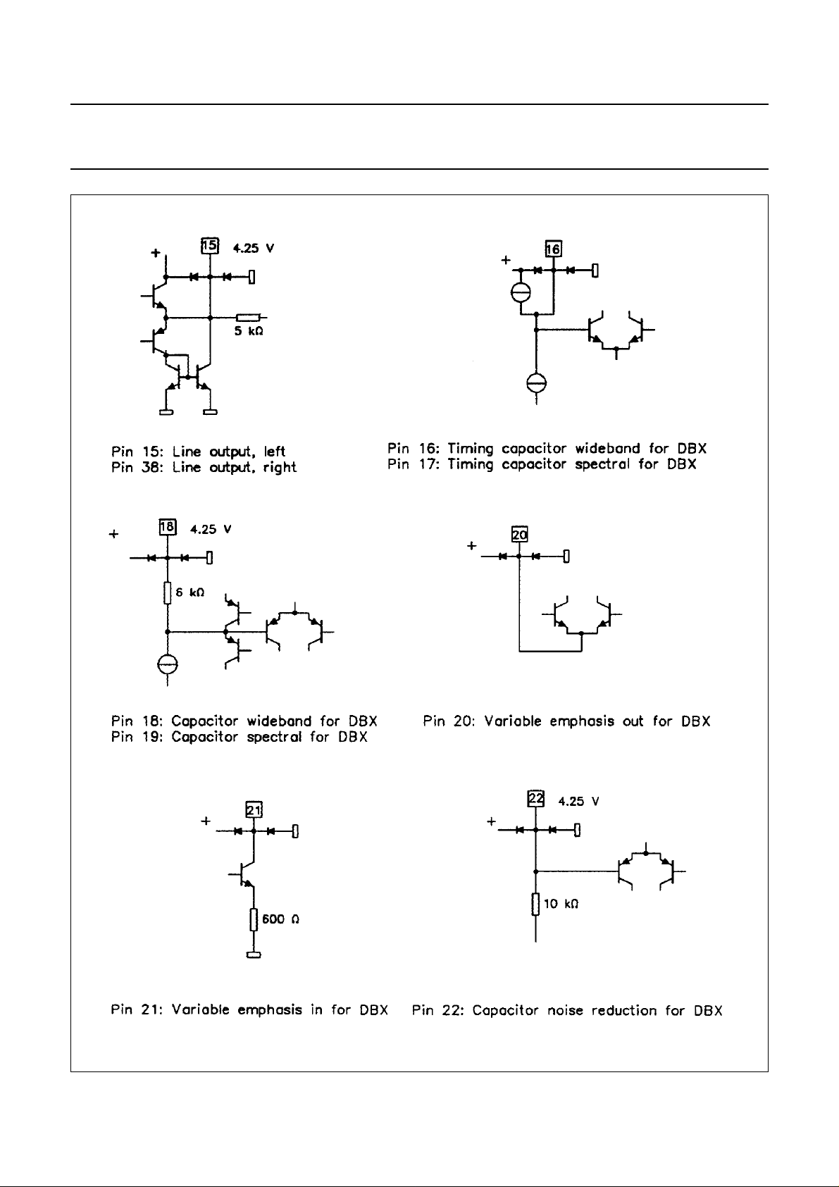
INTERNAL PIN CONFIGURATIONS (pin numbers for SHRDIL-version)
TDA9855
Fig.16 Internal circuits (continued in Fig.17).
July 1994 39
Page 40

Philips Semiconductors Preliminary specification
I2C-bus controlled BTSC stereo / SAP
decoder and audio processor
TDA9855
Fig.17 Internal circuits (continued from Fig.16).
July 1994 40
Page 41
Philips Semiconductors Preliminary specification
I2C-bus controlled BTSC stereo / SAP
decoder and audio processor
TDA9855
Fig.18 Internal circuits (continued from Fig.17).
July 1994 41
Page 42

Philips Semiconductors Preliminary specification
I2C-bus controlled BTSC stereo / SAP
decoder and audio processor
TDA9855
Fig.19 Internal circuits (continued from Fig.18).
July 1994 42
Page 43

Philips Semiconductors Preliminary specification
I2C-bus controlled BTSC stereo / SAP
decoder and audio processor
TDA9855
Fig.20 Internal circuits (continued from Fig.19).
July 1994 43
Page 44

Philips Semiconductors Preliminary specification
I2C-bus controlled BTSC stereo / SAP
decoder and audio processor
TDA9855
Fig.21 Internal circuits (continued from Fig.20).
July 1994 44
Page 45

Philips Semiconductors Preliminary specification
I2C-bus controlled BTSC stereo / SAP
decoder and audio processor
PACKAGE OUTLINES
SDIP52: plastic shrink dual in-line package; 52 leads (600 mil)
D
seating plane
L
Z
e
TDA9855
SOT247-1
M
E
A
2
A
A
1
w M
b
1
c
(e )
M
1
H
52
pin 1 index
1
DIMENSIONS (mm are the original dimensions)
A
A
A
UNIT b
mm
max.
5.08 0.51 4.0
12
min.
max.
b
1.3
0.8
0.53
0.40
b
27
E
26
0 5 10 mm
scale
cEe M
1
0.32
0.23
(1) (1)
D
47.9
47.1
14.0
13.7
e
1
L
M
E
3.2
15.80
2.8
15.24
17.15
15.90
w
H
0.181.778 15.24
Z
max.
1.73
(1)
Note
1. Plastic or metal protrusions of 0.25 mm maximum per side are not included.
OUTLINE
VERSION
SOT247-1
IEC JEDEC EIAJ
REFERENCES
July 1994 45
EUROPEAN
PROJECTION
ISSUE DATE
90-01-22
95-03-11
Page 46

Philips Semiconductors Preliminary specification
I2C-bus controlled BTSC stereo / SAP
decoder and audio processor
PLCC68: plastic leaded chip carrier; 68 leads
e
y
61
68
1
pin 1 index
D
X
4460
TDA9855
SOT188-2
e
E
A
Z
E
43
b
p
b
1
w M
H
E
E
e
A
A
1
A
4
(A )
3
k
9
β
1
27
k
10 26
e
Z
D
H
D
D
v M
A
B
v M
B
0 5 10 mm
scale
DIMENSIONS (millimetre dimensions are derived from the original inch dimensions)
UNIT A
mm
0.180
inches
0.165
A
1
min. max. max. max. max.
4.57
0.51
4.19
0.020
A
0.25
0.01
A
4
3
3.30
0.13
b
p
0.53
0.33
0.021
0.013
b
0.81
0.66
0.032
0.026
1
(1)
D
24.33
24.13
0.958
0.950
(1)
E
eH
e
D
1.27
0.05
23.62
22.61
0.930
0.890
24.33
24.13
0.958
0.950
e
E
23.62
22.61
0.930
0.890
H
D
25.27
25.02
0.995
0.985
25.27
25.02
0.995
0.985
Note
1. Plastic or metal protrusions of 0.01 inches maximum per side are not included.
OUTLINE
VERSION
SOT188-2
IEC JEDEC EIAJ
112E10 MO-047AC
REFERENCES
k
1
k
E
1.22
1.07
0.048
0.042
0.51
0.020
L
1.44
1.02
0.057
0.040
detail X
p
EUROPEAN
PROJECTION
L
p
(1) (1)
Z
Z
E
D
ywv β
0.18 0.100.18
0.007 0.0040.007
2.16
0.085
2.16
0.085
o
45
ISSUE DATE
92-11-17
95-03-11
July 1994 46
Page 47

Philips Semiconductors Preliminary specification
I2C-bus controlled BTSC stereo / SAP
decoder and audio processor
SOLDERING
Introduction
There is no soldering method that is ideal for all IC
packages. Wave soldering is often preferred when
through-hole and surface mounted components are mixed
on one printed-circuit board. However, wave soldering is
not always suitable for surface mounted ICs, or for
printed-circuits with high population densities. In these
situations reflow soldering is often used.
This text gives a very brief insight to a complex technology.
A more in-depth account of soldering ICs can be found in
“IC Package Databook”
our
SDIP
SOLDERING BY DIPPING OR BY WAVE
The maximum permissible temperature of the solder is
260 °C; solder at this temperature must not be in contact
with the joint for more than 5 seconds. The total contact
time of successive solder waves must not exceed
5 seconds.
The device may be mounted up to the seating plane, but
the temperature of the plastic body must not exceed the
specified maximum storage temperature (T
printed-circuit board has been pre-heated, forced cooling
may be necessary immediately after soldering to keep the
temperature within the permissible limit.
R
EPAIRING SOLDERED JOINTS
Apply a low voltage soldering iron (less than 24 V) to the
lead(s) of the package, below the seating plane or not
more than 2 mm above it. If the temperature of the
soldering iron bit is less than 300 °C it may remain in
contact for up to 10 seconds. If the bit temperature is
between 300 and 400 °C, contact may be up to 5 seconds.
(order code 9398 652 90011).
). If the
stg max
TDA9855
Reflow soldering requires solder paste (a suspension of
fine solder particles, flux and binding agent) to be applied
to the printed-circuit board by screen printing, stencilling or
pressure-syringe dispensing before package placement.
Several techniques exist for reflowing; for example,
thermal conduction by heated belt. Dwell times vary
between 50 and 300 seconds depending on heating
method. Typical reflow temperatures range from
215 to 250 °C.
Preheating is necessary to dry the paste and evaporate
the binding agent. Preheating duration: 45 minutes at
45 °C.
W
AVE SOLDERING
Wave soldering techniques can be used for all PLCC
packages if the following conditions are observed:
• A double-wave (a turbulent wave with high upward
pressure followed by a smooth laminar wave) soldering
technique should be used.
• The longitudinal axis of the package footprint must be
parallel to the solder flow.
• The package footprint must incorporate solder thieves at
the downstream corners.
During placement and before soldering, the package must
be fixed with a droplet of adhesive. The adhesive can be
applied by screen printing, pin transfer or syringe
dispensing. The package can be soldered after the
adhesive is cured.
Maximum permissible solder temperature is 260 °C, and
maximum duration of package immersion in solder is
10 seconds, if cooled to less than 150 °C within
6 seconds. Typical dwell time is 4 seconds at 250 °C.
A mildly-activated flux will eliminate the need for removal
of corrosive residues in most applications.
PLCC
REFLOW SOLDERING
Reflow soldering techniques are suitable for all PLCC
packages.
The choice of heating method may be influenced by larger
PLCC packages (44 leads, or more). If infrared or vapour
phase heating is used and the large packages are not
absolutely dry (less than 0.1% moisture content by
weight), vaporization of the small amount of moisture in
them can cause cracking of the plastic body. For more
information, refer to the Drypack chapter in our
Reference Handbook”
July 1994 47
(order code 9397 750 00192).
“Quality
EPAIRING SOLDERED JOINTS
R
Fix the component by first soldering two diagonally-
opposite end leads. Use only a low voltage soldering iron
(less than 24 V) applied to the flat part of the lead. Contact
time must be limited to 10 seconds at up to 300 °C. When
using a dedicated tool, all other leads can be soldered in
one operation within 2 to 5 seconds between
270 and 320 °C.
Page 48

Philips Semiconductors Preliminary specification
I2C-bus controlled BTSC stereo / SAP
TDA9855
decoder and audio processor
DEFINITIONS
Data sheet status
Objective specification This data sheet contains target or goal specifications for product development.
Preliminary specification This data sheet contains preliminary data; supplementary data may be published later.
Product specification This data sheet contains final product specifications.
Limiting values
Limiting values given are in accordance with the Absolute Maximum Rating System (IEC 134). Stress above one or
more of the limiting values may cause permanent damage to the device. These are stress ratings only and operation
of the device at these or at any other conditions above those given in the Characteristics sections of the specification
is not implied. Exposure to limiting values for extended periods may affect device reliability.
Application information
Where application information is given, it is advisory and does not form part of the specification.
LIFE SUPPORT APPLICATIONS
These products are not designed for use in life support appliances, devices, or systems where malfunction of these
products can reasonably be expected to result in personal injury. Philips customers using or selling these products for
use in such applications do so at their own risk and agree to fully indemnify Philips for any damages resulting from such
improper use or sale.
PURCHASE OF PHILIPS I
Purchase of Philips I
components in the I2C system provided the system conforms to the I2C specification defined by
Philips. This specification can be ordered using the code 9398 393 40011.
2
C COMPONENTS
2
C components conveys a license under the Philips’ I2C patent to use the
July 1994 48
 Loading...