

Page 1

INTEGRATED CIRCUITS
DATA SH EET
TDA9855
2
I
C-bus controlled BTSC
stereo/SAP decoder and audio
processor
Product specification
Supersedes data of July 1994
File under Integrated Circuits, IC02
1997 Nov 04
Page 2
Philips Semiconductors Product specification
I2C-bus controlled BTSC stereo/SAP
decoder and audio processor
FEATURES
• Quasi alignment-free BTSC stereo decoder due to
automatic adjustment of channel separation via I2C-bus
• High integration level with automatically tuned
integrated filters
• Input level adjustment I2C-bus controlled
• Alignment-free SAP processing
• dbx noise reduction circuit
• I2C-bus transceiver.
Audio processor
• Selector for internal and external signals (line in)
• Automatic volume level control
• Subwoofer or surround output with separate volume
control
• Volume control
• Special loudness characteristic automatically controlled
in combination with volume setting
• Bass and treble control
• Audio signal zero-crossing detection between any
volume step switching
• Mute control at audio signal zero-crossing.
TDA9855
GENERAL DESCRIPTION
The TDA9855 is a bipolar-integrated BTSC stereo/SAP
decoder with hi-fi audio processor (I2C-bus controlled) for
application in TV sets.
ORDERING INFORMATION
TYPE NUMBER
NAME DESCRIPTION VERSION
TDA9855 SDIP52 plastic shrink dual in-line package; 52 leads (600 mil) SOT247-1
TDA9855WP PLCC68 plastic leaded chip carrier; 68 leads SOT188-2
LICENSE INFORMATION
A license is required for the use of this product. For further information, please contact
COMPANY BRANCH ADDRESS
THAT Corporation Licensing Operations 734 Forest St.
Tokyo Office 405 Palm House, 1-20-2 Honmachi
PACKAGE
Marlborough, MA 01752
USA
Tel.: (508) 229-2500
Fax: (508) 229-2590
Shibuya-ku, Tokyo 151
Japan
Tel.: (03) 3378-0915
Fax: (03) 3374-5191
1997 Nov 04 2
Page 3
Philips Semiconductors Product specification
I2C-bus controlled BTSC stereo/SAP
TDA9855
decoder and audio processor
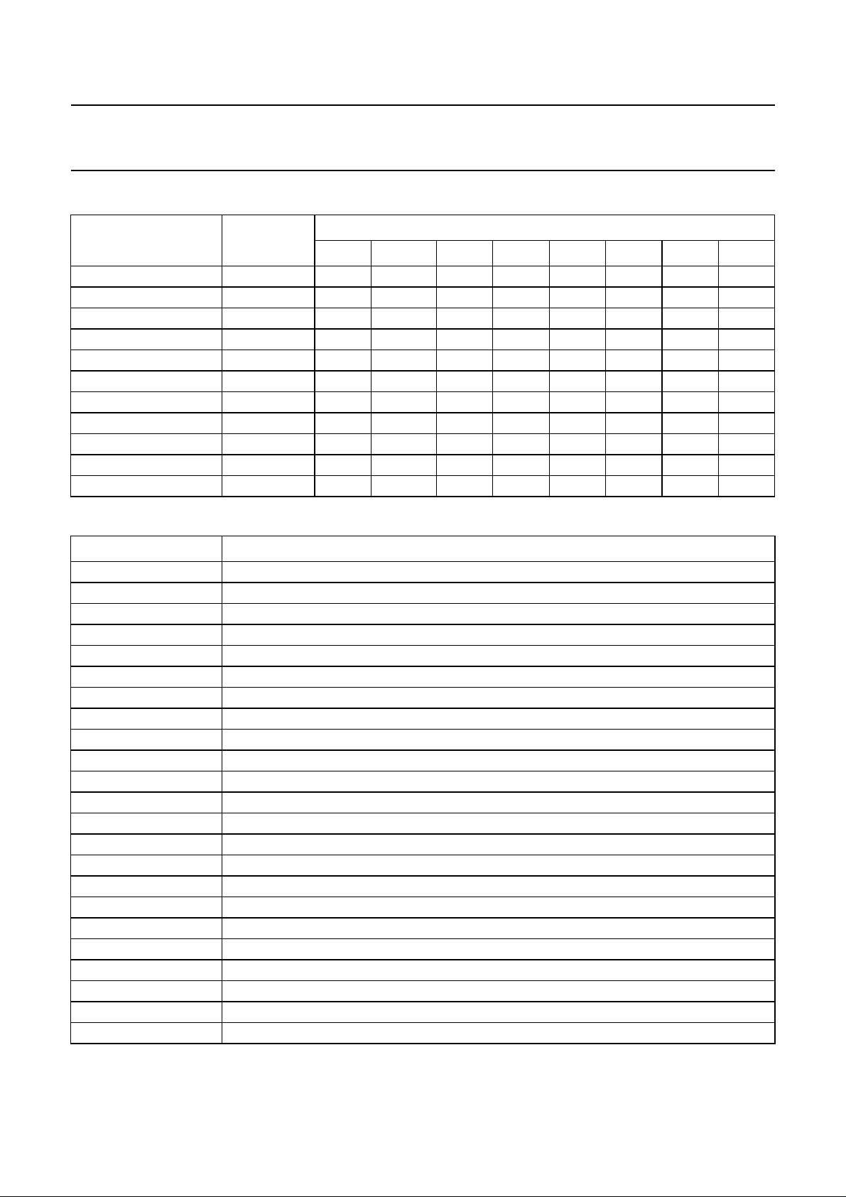
QUICK REFERENCE DATA
SYMBOL PARAMETER CONDITIONS MIN. TYP. MAX. UNIT
V
CC
I
CC
V
COMP(rms)
V
oR,L(rms)
G
LA
α
cs
THD
L,R
V
I, O(rms)
AVL control range −15 − +6 dB
G
c
L
B
G
bass
G
treble
G
s
S/N signal-to-noise ratio line out (mono); V
supply voltage 8.0 8.5 9.0 V
supply current 50 75 95 mA
input signal voltage (RMS value) 100% modulation L + R;
− 250 − mV
fi= 300 Hz
output signal voltage (RMS value) 100% modulation L + R;
− 500 − mV
fi= 300 Hz
input level adjustment control maximum gain − 4 − dB
maximum attenuation −−3.5 − dB
stereo channel separation fL= 300 Hz; fR= 3 kHz 25 35 − dB
total harmonic distortion L + R fi= 1 kHz − 0.2 − %
signal handling (RMS value) THD < 0.5% 2 −−V
volume control range −71 − +16 dB
maximum loudness boost fi=40Hz − 17 − dB
bass control range fi=40Hz −12 − +16.5 dB
treble control range fi= 15 kHz −12 − +12 dB
subwoofer control range fi=40Hz −14 − +14 dB
= 0.5 V (RMS)
o
CCIR noise weighting filter
− 60 − dB
(peak value)
DIN noise weighting filter
− 73 − dBA
(RMS value)
audio section; V
= 2 V (RMS);
o
gain = 0 dB
CCIR noise weighting filter
− 94 − dB
(peak value)
DIN noise weighting filter
− 107 − dBA
(RMS value)
1997 Nov 04 3
Page 4
Philips Semiconductors Product specification
I2C-bus controlled BTSC stereo/SAP
decoder and audio processor
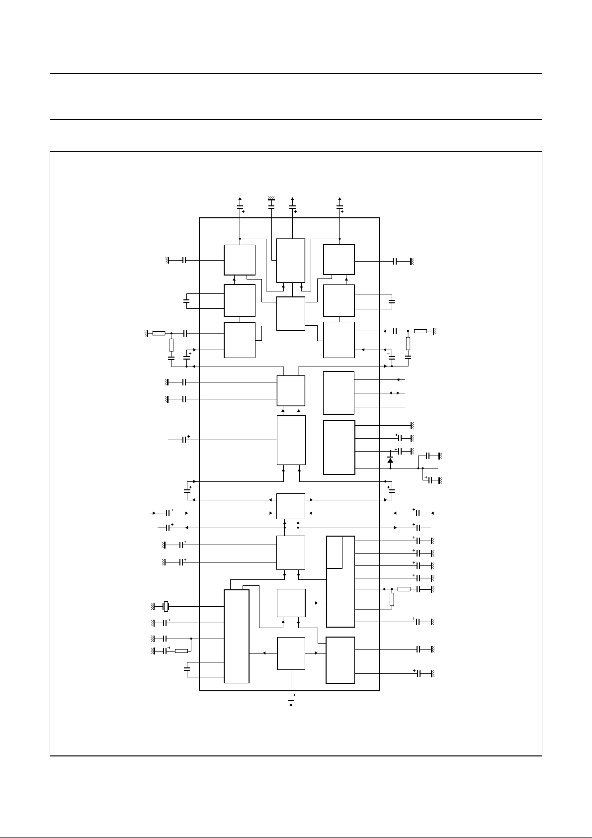
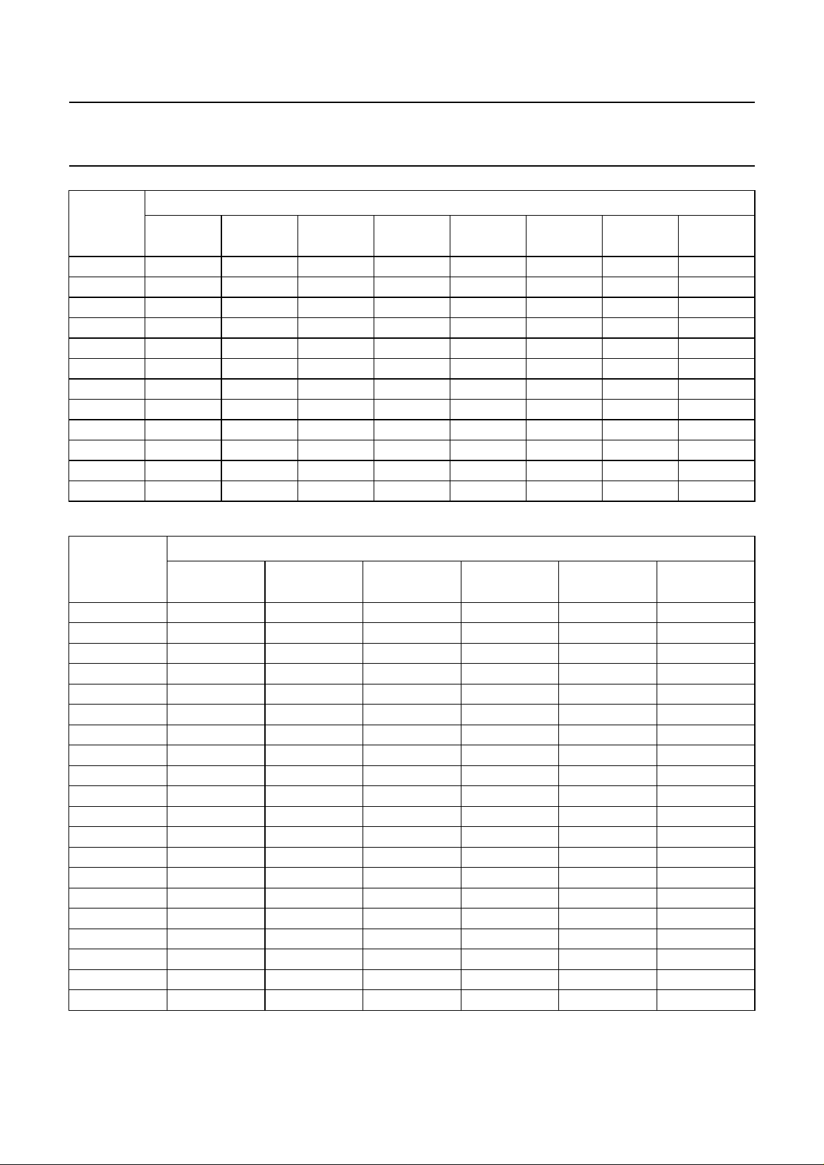
BLOCK DIAGRAM
OUTR
C36
(63) 47
C14
52
handbook, full pagewidth
R3
R2
C11
CC
V
C10
(EIR)
C7
External Input Right
C4 C5
C3
Q1
C20
C16
CERAMIC
C13
C45
C6
RESONATOR
C2
C12
C9
C8
C28
MURATA
R1
(68)
50
(66)
51
(67)
46
(59)
VIR
45
(58)
44
(57)
43
(56)
42
(55)
10
(14)
40
(52)
39
(51)
41
(54)
38
(50)
LOR LIR
37
(49)
36
(48)
CSB503F58
35
(47)
34
(46)
33
(43)
32
(41)
31
(40)
RIGHT
TREBLE
CONTROL
BASS
RIGHT
CONTROL
RIGHT
VOLUME
CONTROL
LOUDNESS
STEREO DECODER
C35
(65) 49
OUTS
C40
(5) 4
MATRIX,
VOLUME
SURROUND
SUBWOOFER
ZERO
CROSSING
TDA9855
EFFECTS
AUTOMATIC
VOLUME AND
LEVEL CONTROL
INPUT
SELECT
+
SELECT
LINEOUT
DEMATRIX
/SAP
SWITCH
STEREO
INPUT
LEVEL
ADJUST
29 (38)
C1
OUTL
C39
(7) 6
LEFT
TREBLE
LEFT
BASS
LEFT
VOLUME
LOUDNESS
C-
2
I
LOGIC,
SUPPLY
ADJUST
STEREO
DBX
SAP
DEMODULATOR
(1)
CONTROL
(4)
(3)
CONTROL
(11)
(12)
CONTROL
(13)
(36)
(35)
(6)
TRANCEIVER
(33,
34)
(15)
(39)
(37)
(18)
(19)
(16)
(20)
(21)
(22)
(23)
(24)
(27)
(25)
(29)
(30)
(31)
TDA9855
MHA837
C33
1
3
C32
2
C31
D1
C29
C26
R5
R4
C30
SCL
SDA
MAD
C15 C34
C49
CC
V
C47
(EIL)
C37 C27
External Input Left
C25C24
C23C22
R7
C21
C19
C18
C17
Fig.1 Block diagram.
7
8
VIL
9
27
28
5
25
11
30
28
13
14
12
15
16
LOL LIL
17
18
19
21
R6
20
22
23
24
1997 Nov 04 4
COMP
The numbers given in parenthesis refer to the TDA9855WP version.
Page 5
Philips Semiconductors Product specification
I2C-bus controlled BTSC stereo/SAP
TDA9855
decoder and audio processor
Component list
Electrolytic capacitors ±20%; foil or ceramic capacitors ±10%; resistors ±5%; unless otherwise specified; see Fig.1.
COMPONENTS VALUE TYPE REMARK
C1 10 µF electrolytic 63 V
C2 470 nF foil −
C3 4.7 µF electrolytic 63 V
C4 220 nF foil −
C5 10 µF electrolytic 63 V; I
C6 2.2 µF electrolytic 16 V
C7 4.7 µF electrolytic 16 V
C8 15 nF foil ±5%
C9 15 nF foil ±5%
C10 2.2 µF electrolytic 63 V
C11 8.2 nF foil or ceramic ±5% SMD 2220/1206
C12 150 nF foil ±5%
C13 33 nF foil ±5%
C14 5.6 nF foil or ceramic ±5% SMD 2220/1206
C15 100 µF electrolytic 16 V
C16 4.7 µF electrolytic 63 V
C17 4.7 µF electrolytic 63 V
C18 100 nF foil
C19 10 µF electrolytic 63 V
C20 4.7 µF electrolytic 63 V
C21 47 nF foil ±5%
C22 1 µF electrolytic 63 V
C23 1 µF electrolytic 63 V
C24 10 µF electrolytic 63 V ±10%
C25 10 µF electrolytic 63 V ±10%
C26 2.2 µF electrolytic 16 V
C27 2.2 µF electrolytic 63 V
C28 4.7 µF electrolytic 63 V ±10%
C29 2.2 µF electrolytic 16 V
C30 8.2 nF foil or ceramic ±5% SMD 2220/1206
C31 150 nF foil ±5%
C32 33 nF foil ±5%
C33 5.6 nF foil or ceramic ±5% SMD 2220/1206
C34 100 µF electrolytic 16 V
C35 150 nF foil ±5%
C36 4.7 µF electrolytic 16 V
C37 4.7 µF electrolytic 16 V
C39 4.7 µF electrolytic 16 V
C40 4.7 µF electrolytic 16 V
leak
< 1.5 µA
1997 Nov 04 5
Page 6
Philips Semiconductors Product specification
I2C-bus controlled BTSC stereo/SAP
decoder and audio processor
COMPONENTS VALUE TYPE REMARK
C45 2.2 µF electrolytic 16 V
C47 220 µF electrolytic 25 V
C49 100 nF foil or ceramic SMD 1206
D1 −−general purpose diode
R1 2.2 kΩ− −
R2 20 kΩ− −
R3 2.2 kΩ− −
R4 20 kΩ− −
R5 2.2 kΩ− −
R6 8.2 kΩ− ±2%
R7 160 Ω− ±2%
Q1 CSB503F58 radial leads
CSB503JF958 alternative as SMD
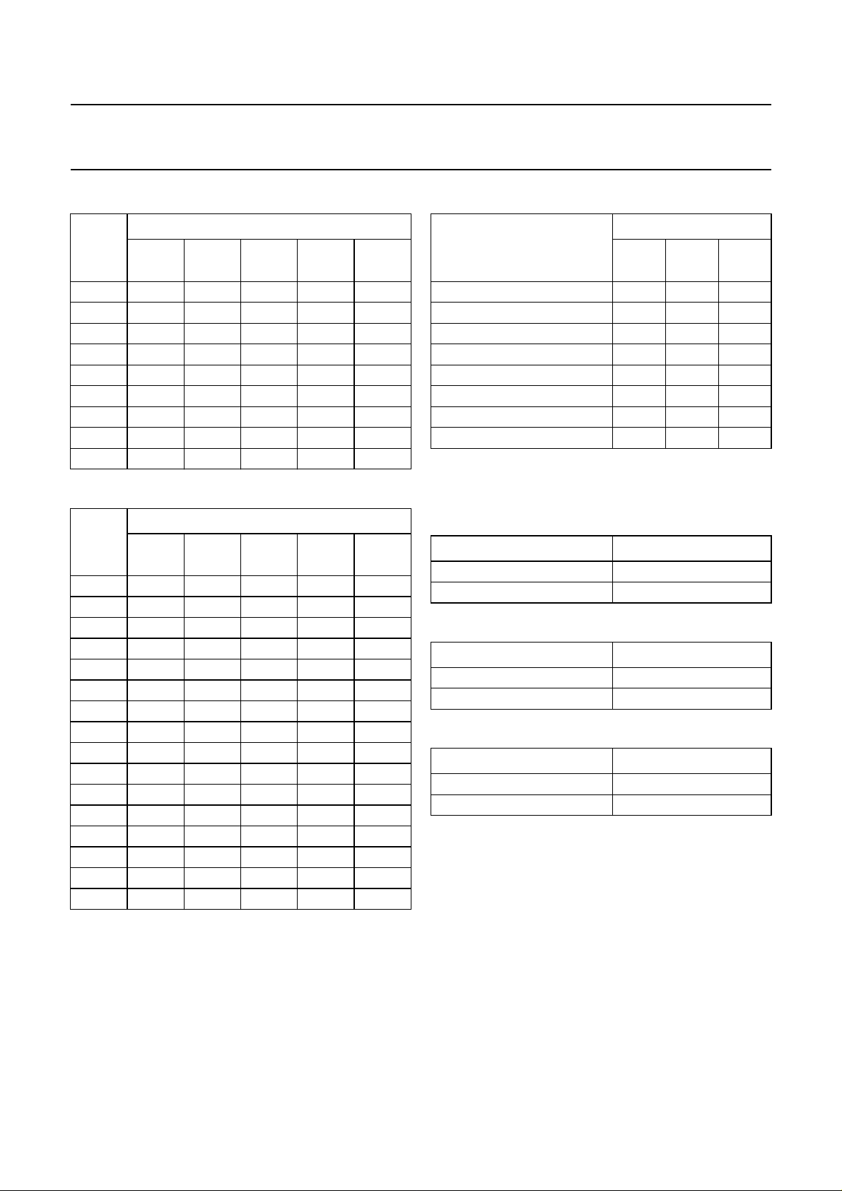
PINNING
TDA9855
SYMBOL
DESCRIPTION
PLCC68 SDIP52
TL 1 1 treble control capacitor, left channel
n.c. 2 − not connected
B1L 3 2 bass control capacitor, left channel
B2L 4 3 bass control capacitor, left channel
OUTS 5 4 output subwoofer or output surround sound
MAD 6 5 programmable address bit (module address)
OUTL 7 6 output, left channel
n.c. 8 to 10 − not connected
LDL 11 7 input loudness, left channel
VIL 12 8 input volume control, left channel
EOL 13 9 output effects, left channel
PINS
C
AV
V
ref
14 10 automatic volume control capacitor
15 11 reference voltage 0.5V
CC
LIL 16 12 input line, left channel
n.c. 17 − not connected
AVL 18 13 input automatic volume control, left channel
SOL 19 14 output selector, left channel
LOL 20 15 output line control, left channel
C
TW
C
TS
C
W
C
S
21 16 capacitor timing wideband for dbx
22 17 capacitor timing spectral for dbx
23 18 capacitor wideband for dbx
24 19 capacitor spectral for dbx
VEO 25 20 variable emphasis output for dbx
1997 Nov 04 6
Page 7
Philips Semiconductors Product specification
I2C-bus controlled BTSC stereo/SAP
TDA9855
decoder and audio processor
SYMBOL
PLCC68 SDIP52
n.c. 26 − not connected
VEI 27 21 variable emphasis input for dbx
n.c. 28 − not connected
C
NR
C
M
C
DEC
29 22 capacitor noise reduction for dbx
30 23 capacitor mute for SAP
31 24 capacitor DC-decoupling for SAP
n.c. 32 − not connected
AGND 33 − analog ground
DGND 34 − digital ground
GND − 25 ground
SDA 35 26 serial data input/output (I
SCL 36 27 serial clock input (I
V
CC
37 28 supply voltage
COMP 38 29 composite input signal
V
C
C
CAP
P1
P2
39 30 capacitor for electronic filtering of supply
40 31 capacitor for pilot detector
41 32 capacitor for pilot detector
n.c. 42 − not connected
C
PH
43 33 capacitor for phase detector
n.c. 44, 45 − not connected
C
ADJ
46 34 capacitor for filter adjustment
CER 47 35 ceramic resonator
C
MO
C
SS
48 36 capacitor DC-decoupling mono
49 37 capacitor DC-decoupling stereo/SAP
LOR 50 38 output line control, right channel
SOR 51 39 output selector, right channel
AVR 52 40 input automatic volume control, right channel
n.c. 53 − not connected
LIR 54 41 input line control, right channel
C
PS2
C
PS1
55 42 capacitor 2 pseudo function
56 43 capacitor 1 pseudo function
EOR 57 44 output effects, right channel
VIR 58 45 input volume control, right channel
LDR 59 46 input loudness, right channel
n.c. 60 to 62 − not connected
OUTR 63 47 output, right channel
n.c. 64 48 not connected
SW 65 49 filter capacitor for subwoofer
PINS
DESCRIPTION
2
C-bus)
2
C-bus)
1997 Nov 04 7
Page 8
Philips Semiconductors Product specification
I2C-bus controlled BTSC stereo/SAP
decoder and audio processor
n.c.
8
PINS
OUTL
7
MAD
6
OUTS
5
B2L
4
n.c.
B1L
3
2
TDA9855H
TL
DESCRIPTION
TR
B1R
B2RSWn.c.
1
68
67
66
65
OUTR
64
63
n.c.
62
n.c.
61
SYMBOL
PLCC68 SDIP52
B2R 66 50 bass control capacitor, right channel
B1R 67 51 bass control capacitor, right channel
TR 68 52 treble control capacitor
handbook, full pagewidth
n.c.
9
10
n.c.
11
LDL
12
VIL
13
EOL
C
14
AV
V
15
ref
16
LIL
17
n.c.
18
AVL
19
SOL
20
LOL
C
21
TW
C
22
TS
23
C
W
C
24
S
25
VEO
26
n.c.
TDA9855
60
n.c.
59
LDR
58
VIR
57
EOR
C
56
PS1
C
55
PS2
54
LIR
53
n.c.
52
AVR
51
SOR
50
LOR
C
49
SS
C
48
MO
47
CER
C
46
ADJ
45
n.c.
44
n.c.
27
28
29
30
31
32
33
34
M
NR
VEI
n.c.
C
C
DEC
C
n.c.
AGND
DGND
Fig.2 Pin configuration (PLCC version).
1997 Nov 04 8
35
SDA
36
SCL
V
37
CC
38
COMP
39
CAP
V
40
CP1C
41
42
43
P2
n.c.
MHA836
PH
C
Page 9
Philips Semiconductors Product specification
I2C-bus controlled BTSC stereo/SAP
decoder and audio processor
handbook, halfpage
TL TR
1
B1L B1R
2
B2L B2R
3
OUTS SW
4
MAD n.c.
5
OUTL OUTR
6
LDL LDR
7
VIL VIR
8
EOL EOR
9
C
10
AV
V
11
ref
LIL LIR
12
AVL AVR
13
52
51
50
49
48
47
46
45
44
C
43
PS1
C
42
PS2
41
40
TDA9855
SOL SOR
14
LOL LOR
15
C
16
TW
C
17
TS
C
18
W
C
19
s
VEO
20
VEI
21
C
22
NR
C
23
M
C
24
DEC
GND
25
SDA SCL
26
MHA835
39
38
C
37
SS
C
36
MO
CER
35
C
34
ADJ
C
33
PH
C
32
P2
C
31
P1
V
30
CAP
COMP
29
V
28
CC
27
TDA9855
FUNCTIONAL DESCRIPTION
Decoder
NPUT LEVEL ADJUSTMENT
I
The composite input signal is fed to the input level
adjustment stage. In order to compensate tolerances of
the FM demodulator which supplied the composite input
signal, the TDA9855 provides an input level adjustment
stage. The control range is from−3.5 to +4.0 dB in steps of
0.5 dB. The subaddress control 3 of Tables 5 and 6 and
the level adjust setting of Table 22 allows an optimum
signal adjustment during the set alignment in the
production line. This value has to be stored in a
non-volatile memory. The maximum input signal voltage is
2 V (RMS).
TEREO DECODER
S
The output signal of the level adjustment stage is coupled
to a low-pass filter which suppresses the baseband noise
above 125 kHz. The composite signal is then fed into a
pilot detector/pilot cancellation circuit and into the MPX
demodulator. The main L + R signal passes a 75 µs fixed
de-emphasis filter and is fed into the dematrix circuit.
The decoded sub-signal L − R is sent to the stereo/SAP
switch. To generate the pilot signal the stereo demodulator
uses a PLL circuit including a ceramic resonator.
The stereo channel separation can be adjusted by an
automatic procedure or manually. For a detailed
description see Section “Adjustment procedure”.
The stereo identification can be read by the I2C-bus
(see Table 2). Two different pilot thresholds can be
selected via the I2C-bus (see Table 24).
DEMODULATOR
SAP
The composite signal is fed from the output of the input
level adjustment stage to the SAP demodulator circuit
through a 5fH (fH= horizontal frequency) band-pass filter.
The demodulator level is automatically controlled.
The SAP demodulator includes internal noise and field
strength detectors that mute the SAP output in the event of
insufficient signal conditions. The SAP identification signal
can be read by the I2C-bus (see Table 2).
S
WITCH
Fig.3 Pin configuration (SDIP version).
1997 Nov 04 9
The stereo/SAP switch feeds either the L − R signal or the
SAP demodulator output signal via the internal dbx noise
reduction circuit to the dematrix/line out select circuit.
Table 21 shows the different switch modes provided at the
output pins LOR and LOL.
Page 10

Philips Semiconductors Product specification
I2C-bus controlled BTSC stereo/SAP
decoder and audio processor
dbx DECODER
The circuit includes all blocks required for the noise
reduction system in accordance with the BTSC system
specification. The output signal is fed through a 73 µs fixed
de-emphasis circuit to the dematrix block.
I
NTEGRATED FILTERS
The filter functions necessary for stereo and SAP
demodulation and part of the dbx filter circuits are provided
on-chip using transconductor circuits. The required filter
accuracy is attained by an automatic filter alignment
circuit.
Audio processor
SELECTOR
The selector allows selecting either the internal line out
signals LOR or LOL (dematrix output) or the external line
in signals LIR and LIL and combines the left and right
signals in several modes (see Table 12). The input signal
capability of the line inputs (LIR/LIL) is 2 V (RMS).
The output of the selector is AC-coupled to the automatic
volume level control circuit via pins SOR/SOL and
AVR/AVL to avoid offset voltages.
A
UTOMATIC VOLUME LEVEL CONTROL
The automatic volume level stage controls its output
voltage to a constant level of typically 200 mV (RMS) from
an input voltage range of 0.1 to 1.1 V (RMS). The circuit
adjusts variations in modulation during broadcasting and
due to changes in the programme material. The function
can be switched off. To avoid audible ‘plops’ during the
permanent operation of the AVL circuit a soft blending
scheme has been applied between the different gain
stages. A capacitor (4.7 µF) at pin CAV determines the
attack and decay time constants. In addition the ratio of
attack and decay time can be changed via the I2C-bus
(see notes 7 and 8 of Chapter “Characteristics”).
E
FFECTS
The audio processor section offers the following mode
selections: linear stereo, pseudo stereo, spatial stereo and
forced mono.The spatial mode provides an antiphase
crosstalk of 30% or 52% (switchable via the I2C-bus;
see Table 18).
OLUME/LOUDNESS
V
The volume control range is from +16 dB to −71 dB in
steps of 1 dB and ends with a mute step (see Table 8).
Balance control is achieved by the independent volume
TDA9855
control of each channel. The volume control blocks
operate in combination with the loudness control. The filter
is linear when maximum gain for volume control is
selected. The filter characteristic changes automatically
over a range of 28 dB down to a setting of −12 dB.
At −12 dB volume control the maximum loudness boost is
obtained. The filter characteristic is determined by external
components. The proposed application provides a
maximum boost of 17 dB for bass and 4.5 dB for treble.
The loudness may be switched on or off via I
control (see Table 14). The left and right volume control
stages include two independent zero-crossing detectors.
In the zero-crossing mode a change in volume is
automatically activated but not executed. The execution is
enabled at the next zero-crossing of the signal. If a new
volume step is activated before the previous one has been
processed, the previous value will be executed first, and
then the new value will be activated. If no zero-crossing
occurs the next volume transmission will enforce the last
activated volume setting.
The zero-crossing mode is realized between adjoining
steps and between any steps, but not from any step to
mute. In this case the GMU bit is required for use. In case
only one channel has to be muted, two steps are
necessary. The first step is a transmission of any step to
−71 dB and the second step is the −71 dB step to mute
mode. The step of −71 dB to mute mode has no
zero-crossing but this is not relevant. This procedure has
to be provided by software.
B
ASS CONTROL
A single external 33 nF capacitor for each channel in
combination with a linear operational amplifier and internal
resistors provides a bass control range of +16.5 to −12 dB
in steps of 1.5 dB at low frequencies (40 Hz). Internally the
basic step width is 3 dB, with intermediate steps obtained
by a toggle function that provides an additional 1.5 dB
boost or attenuation (see Table 9). It should be noted that
both loudness and bass control together result in a
maximum bass boost of 34.5 dB for low volume steps.
T
REBLE CONTROL
The adjustable range of the treble control stage is from
−12 to +12 dB in steps of 3 dB. The filter characteristic is
determined by an external 5.6 nF capacitor for each
channel. The logic circuitry is arranged in a way that the
same data words (06H to 16H) can be used for both tone
controls if a bass control range from −12 to +12 dB and a
treble control range from −12 to +12 dB with 3 dB steps
are used (see Tables 9 and 10).
2
C-bus
1997 Nov 04 10
Page 11

Philips Semiconductors Product specification
I2C-bus controlled BTSC stereo/SAP
decoder and audio processor
SUBWOOFER; SURROUND SOUND CONTROL
The subwoofer or the surround mode can be activated with
the control bit SUR (see Table 6). A low bit provides an
output signal1⁄2(L + R) in subwoofer mode, a high bit
selects surround mode and provides an output signal
1
⁄2(L − R). The signal is fed through a volume control stage
with a range from +14 to −14 dB in 2 dB steps on top of the
main channel control to the output pin OUTS. The last
setting is the mute position (see Table 11). The capacitor
C35 at pin SW provides a 230 Hz low-pass filter in
subwoofer mode. In surround mode this capacitor should
be disconnected. If balance is not in mid position the
selected left and right output levels will be combined.
M
UTE
The mute function can be activated independently with the
last step of volume or subwoofer/surround control at the
left, right or centre output. By setting the general mute bit
GMU via the I2C-bus all audio part outputs are muted.
All channels include an independent zero-crossing
detector. The zero-crossing mute feature can be selected
via bit TZCM:
TZCM = 0: forced mute with direct execution
TZCM = 1: execution in time with signal zero-crossing.
In the zero-crossing mode a change of the GMU bit is
activated but not executed. The execution is enabled at
the next zero-crossing of the signal. To avoid a large delay
of mute switching, when very low frequencies are
processed, or the output signal amplitude is lower than the
DC offset voltage, the following I2C-bus transmissions are
needed:
A first transmission for mute execution
A second transmission approximately 100 ms later,
which must switch the zero-crossing mode to forced
mute (TZCM = 0)
A third transmission to reactivate the zero-crossing
mode (TZCM = 1). This transmission can take place
immediately, but must follow before the next mute
execution.
Adjustment procedure
COMPOSITE INPUT LEVEL ADJUSTMENT
Apply the composite signal (from the FM demodulator)
with 100% modulation (25 kHz deviation) L + R;
fi= 300 Hz. Set input level control via the I2C-bus
monitoring line output (500 mV ±20 mV). Store the setting
in a non-volatile memory. Adjustment of the spectral and
TDA9855
wideband expander is performed via the stereo channel
separation adjust.
UTOMATIC ADJUSTMENT PROCEDURE
A
• Capacitors of external inputs EIL and EIR must be
grounded
• Composite input signal L = 300 Hz, R = 3.1 kHz,
14% modulation for each channel; volume gain +16 dB
via the I2C-bus; to avoid annoying sound level set GMU
bit to logic 1 during adjustment procedure
• Effects, AVL, loudness off
• Selector setting SC0, SC1 and SC2 = 0, 0, 0
(see Table 12)
• Line out setting bits: STEREO = 1, SAP = 0
(see Table 21)
• Start adjustment by transmission ADJ = 1 in register
ALI3; the decoder will align itself
• After 1 second, stop alignment by transmitting ADJ = 0
in register ALI3 read the alignment data by an I
read operation from ALR1 and ALR2
(see Chapter “I2C-bus protocol”) and store it in a
non-volatile memory; the alignment procedure
overwrites the previous data stored in ALI1 and ALI2
• Disconnect the capacitors of external inputs from
ground.
M
ANUAL ADJUSTMENT
Manual adjustment is necessary when no dual tone
generator is available (e.g. for service).
• Spectral and wideband data have to be set to 10000
(middle position for adjustment range)
• Composite input L = 300 Hz; 14% modulation
• Adjust channel separation by varying wideband data
• Composite input L = 3 kHz; 14% modulation
• Adjust channel separation by varying spectral data
• Iterative spectral/wideband operation for optimum
adjustment
• Store data in non-volatile memory.
After every power-on, the alignment data and the input
level adjustment data must be loaded from the non-volatile
memory.
T
IMING CURRENT FOR RELEASE RATE
Due to possible internal and external spreading, the timing
current can be adjusted via the I2C-bus (see Table 25) as
recommended by dbx.
2
C-bus
1997 Nov 04 11
Page 12
Philips Semiconductors Product specification
I2C-bus controlled BTSC stereo/SAP
TDA9855
decoder and audio processor
Requirements for the composite input signal to ensure correct system performance
SYMBOL PARAMETER CONDITIONS MIN. TYP. MAX. UNIT
COMP
L+R(rms)
composite input level for 100%
modulation L + R;
25 kHz deviation;
fi= 300 Hz; RMS value
∆COMP composite input level
spreading under operating
conditions
Z
o
f
lf
f
hf
THD
L,R
output impedance note 1 − low-ohmic 5 kΩ
low frequency roll-off 25 kHz deviation L + R; −2dB −− 5Hz
high frequency roll-off 25 kHz deviation L + R; −2 dB 100 −−kHz
total harmonic distortion L + R fi= 1 kHz; 25 kHz deviation −− 0.5 %
S/N signal-to-noise ratio
L + R/noise
α
SB
side band suppression mono
into unmodulated SAP carrier;
SAP carrier/side band
α
SP
spectral spurious attenuation
L + R/spurious
measured at pin COMP 162 250 363 mV
T
= −20 to +70 °C; aging;
amb
−0.5 − +0.5 dB
power supply influence
f
= 1 kHz; 125 kHz deviation;
i
−− 1.5 %
note 2
CCIR 468-2 weighted quasi
peak; L + R; 25 kHz deviation;
f
= 1 kHz; 75 µs de-emphasis
i
critical picture modulation 44 −−dB
with sync only 54 −−dB
mono signal: 25 kHz deviation,
46 −−dB
fi= 1 kHz; side band: SAP
carrier frequency ±1 kHz
50 Hz to 100 kHz;
40 −−dB
mainly n × fH; no de-emphasis;
L + R; 25 kHz deviation,
f = 1 kHz as reference
Notes
1. Low-ohmic preferred, otherwise the signal loss and spreading at COMP, caused by Z
and the composite input
o
impedance (see Chapter “Characteristics”, Section INPUT LEVEL ADJUSTMENT CONTROL) must be taken into
account.
2. In order to prevent clipping at over-modulation (maximum deviation in the BTSC system for 100% modulation is
73 kHz).
1997 Nov 04 12
Page 13
Philips Semiconductors Product specification
I2C-bus controlled BTSC stereo/SAP
TDA9855
decoder and audio processor
LIMITING VALUES
In accordance with the Absolute Maximum Rating System (IEC 134).
SYMBOL PARAMETER CONDITIONS MIN. MAX. UNIT
V
CC
V
n
T
amb
T
stg
V
esd
Notes
1. Human body model: C = 100 pF; R = 1.5 kΩ.
2. Charge device model: C = 200 pF; R = 0 Ω.
THERMAL CHARACTERISTICS
SYMBOL PARAMETER CONDITIONS VALUE UNIT
R
th(j-a)
supply voltage 0 9.5 V
voltage of all other pins with respect to pin
GND
operating ambient temperature −20 +70 °C
storage temperature −65 +150 °C
electrostatic handling note 1 −2000 +2000 V
note 2 −300 +300 V
thermal resistance from junction to ambient in free air
SOT247-1 43 K/W
SOT188-2 38 K/W
0VCCV
1997 Nov 04 13
Page 14
Philips Semiconductors Product specification
I2C-bus controlled BTSC stereo/SAP
TDA9855
decoder and audio processor
CHARACTERISTICS
All voltages are measured relative to GND; VCC= 8.5 V; source resistance Rs≤ 600 Ω; output load RL≥ 10 kΩ;
CL≤ 2.5 nF; AC-coupled; fi= 1 kHz; T
loudness off; AVL off; effects linear; composite input signal in accordance with BTSC standard; see Fig.1;
unless otherwise specified.
SYMBOL PARAMETER CONDITIONS MIN. TYP. MAX. UNIT
General
V
CC
I
CC
V
DC
supply voltage 8.0 8.5 9.0 V
supply current 50 75 95 mA
DC voltage at signal handling
pins
Decoder section
I
NPUT LEVEL ADJUSTMENT CONTROL
G
G
V
LA
step
i(rms)
input level adjustment control maximum gain − 4.0 − dB
step resolution − 0.5 − dB
maximum input voltage level
(RMS value)
Z
i
input impedance 29.5 35 40.5 kΩ
STEREO DECODER
MPX
L+R(rms)
input voltage level for 100%
modulation L + R; 25 kHz
deviation (RMS value)
MPX
L−R
input voltage level for 100%
modulation L − R; 50 kHz
deviation (peak value)
MPX
(max)
maximum headroom for L + R,
L, R
MPX
pilot(rms)
nominal stereo pilot voltage
level (RMS value)
ST
on(rms)
pilot threshold voltage stereo
on (RMS value)
ST
off(rms)
pilot threshold voltage stereo
off (RMS value)
hys hysteresis − 2.5 − dB
OUT
L+R
output voltage level for 100%
modulation L + R at LINE OUT
=25°C; volume gain control Gc= 0 dB; bass linear; treble linear;
amb
−
1
⁄2V
CC
maximum attenuation −−3.5 − dB
2 −−V
input level adjusted via I2C-bus
− 250 − mV
(L + R; fi= 300 Hz);
monitoring line out
− 707 − mV
f
< 15 kHz; THD < 15% for
mod
9 −−dB
75 µs equivalent input
modulation
− 50 − mV
data STS = 1 −− 35 mV
data STS = 0 −− 30 mV
data STS = 1 15 −−mV
data STS = 0 10 −−mV
input level adjusted via I2C-bus
480 500 520 mV
(L + R; fi= 300 Hz);
monitoring LINE OUT
− V
1997 Nov 04 14
Page 15
Philips Semiconductors Product specification
I2C-bus controlled BTSC stereo/SAP
TDA9855
decoder and audio processor
SYMBOL PARAMETER CONDITIONS MIN. TYP. MAX. UNIT
α
cs
f
L, R
THD
L,R
S/N signal-to-noise ratio mono mode; CCIR 468-2
TEREO DECODER, OSCILLATOR (VCXO); note 1
S
f
o
f
of
∆f
H
SAP DEMODULATOR; note 2
SAP
i(rms)
SAP
on(rms)
SAP
off(rms)
SAP
hys
SAP
LEV
f
res
THD total harmonic distortion f
stereo channel separation L/R
at LINE OUT
aligned with dual tone 14%
modulation; see Section
“Adjustment procedure” in
Chapter “Functional
description”
= 300 Hz; fR= 3 kHz 25 35 − dB
f
L
f
= 300 Hz; fR= 8 kHz 20 30 − dB
L
f
= 300 Hz; fR= 10 kHz 15 25 − dB
L
L, R frequency response 14% modulation;
f
= 300 Hz L or R
ref
=50Hzto11kHz −3 −−dB
f
i
f
= 12 kHz −−3 −dB
i
total harmonic distortion L, R
at LINE OUT
modulation L or R
1% to 100%; fi= 1 kHz
− 0.2 1.0 %
50 60 − dB
weighted; quasi peak;
500 mV output signal
nominal VCXO output
frequency (32fH)
spread of free-running
frequency
capture range frequency
with nominal ceramic
resonator
with nominal ceramic
resonator
− 503.5 − kHz
500.0 − 507.0 kHz
±190 ±265 − Hz
(nominal pilot)
nominal SAP carrier input
voltage level (RMS value)
pilot threshold voltage SAP on
15 kHz frequency deviation of
intercarrier
− 150 − mV
−− 85 mV
(RMS value)
pilot threshold voltage SAP off
35 −−mV
(RMS value)
hysteresis − 2 − dB
SAP output voltage level at
LINE OUT
LINE OUT (LOL, LOR) in
position SAP/SAP;
f
= 300 Hz;
mod
− 500 − mV
100% modulation
frequency response 14% modulation;
50 Hz to 8 kHz; f
= 1 kHz − 0.5 2.0 %
i
= 300 Hz
ref
−3 −−dB
1997 Nov 04 15
Page 16
Philips Semiconductors Product specification
I2C-bus controlled BTSC stereo/SAP
TDA9855
decoder and audio processor
SYMBOL PARAMETER CONDITIONS MIN. TYP. MAX. UNIT
LINE OUT AT PINS LOL AND LOR
V
o(rms)
nominal output voltage
(RMS value)
HEAD
o
Z
o
V
O
R
L
C
L
α
ct
output headroom 9 −−dB
output impedance − 80 120 Ω
DC output voltage 0.45VCC0.5V
output load resistance 5 −−kΩ
output load capacitance −− 2.5 nF
idle crosstalk L, R into SAP 100% modulation; fi= 1 kHz;
idle crosstalk SAP into L, R 100% modulation; f
∆V
ST-SAP
output voltage difference if
switched from L, R to SAP
dbx NOISE REDUCTION CIRCUIT
t
adj
I
s
stereo adjustment time see Section “Adjustment
nominal timing current for
nominal release rate of
spectral RMS detector
∆I
s
I
s(range)
spread of timing current −− 15 %
timing current adjustment
range
I
t
timing current for release rate
of wideband RMS detector
Rel
rate
nominal RMS detector
release rate
100% modulation − 500 − mV
CC
0.55VCCV
50 −−dB
L or R; line out switched to
SAP/SAP
= 1 kHz;
i
50 −−dB
SAP; line out switched to
stereo
250 Hz to 6.3 kHz −− 3dB
−− 1s
procedure” in Chapter
“Functional description”
Is can be measured at pin 17
− 24 −µA
(pin 22) via current meter
connected to1⁄2VCC+1V
7 steps via I2C-bus −±30 − %
−
1
⁄3I
s
−µA
nominal timing current and
external capacitor values
wideband − 125 − dB/s
spectral − 381 − dB/s
1997 Nov 04 16
Page 17
Philips Semiconductors Product specification
I2C-bus controlled BTSC stereo/SAP
TDA9855
decoder and audio processor
SYMBOL PARAMETER CONDITIONS MIN. TYP. MAX. UNIT
Audio part
CIRCUIT SECTION FROM PINS LIL AND LIR TO PINS OUTL, OUTR AND OUTS; note 3
B roll-off frequencies C
6,C7,C10,C26,C27
C29= 2.2 µF; Zi=Z
low frequency (−3 dB) −− 20 Hz
high frequency (−0.5 dB) 20 −−kHz
THD total harmonic distortion Vi= 1 V (RMS); Gc= 0 dB;
AVL on
V
= 2 V (RMS); Gc= 0 dB;
i
AVL on
V
= 1 V (RMS); Gc= 0 dB;
i
AVL off
V
= 2 V (RMS); Gc= 0 dB;
i
AVL off
PSRR power supply ripple rejection V
α
B
crosstalk between bus inputs
notes 4 and 5 − 110 − dB
< 200 mV; fi= 100 Hz 47 50 − dB
r(rms)
and signal outputs
V
no
noise output voltage CCIR 468-2 weighted;
quasi peak
measured in dBA − 8 −µV
αcschannel separation Vi=1V; fi= 1 kHz 75 −−dB
V
=1V; fi= 12.5 kHz 75 −−dB
i
SELECTOR (FROM PINS LOL, LOR, LIL AND LIR TO PINS SOL AND SOR)
Z
α
V
i
s
i(rms)
input impedance 16 20 24 kΩ
input isolation of one selected
source to any other input
maximum input voltage
f = 1 kHz; Vi=1V 86 96 − dB
f = 12.5 kHz; V
THD < 0.5% 2 2.3 − V
(RMS value)
V
offset
DC offset voltage at selector
output by selection of any
inputs
Z
o
R
L
C
L
G
c
output impedance − 80 120 Ω
output load resistance (AC) 5 −−kΩ
output load capacitance −− 2.5 nF
voltage gain, selector − 0 − dB
and
i(min)
− 0.2 0.5 %
− 0.2 0.5 %
− 0.05 − %
− 0.02 − %
− 40 80 µV
=1V 80 96 − dB
i
−− 25 mV
1997 Nov 04 17
Page 18

Philips Semiconductors Product specification
I2C-bus controlled BTSC stereo/SAP
TDA9855
decoder and audio processor
SYMBOL PARAMETER CONDITIONS MIN. TYP. MAX. UNIT
AUTOMATIC VOLUME LEVEL CONTROL (AVL)
Z
i
V
i(rms)
G
v
G
step
V
i(rms)
V
o(rms)
V
DC(OFF)
R
att
I
dec
EFFECT CONTROLS
α
spat1
α
spat2
ϕ phase shift by pseudo-stereo see Fig.5 −− −−
V
OLUME TONE CONTROL PART (INPUT PINS VIL AND VIR TO PINS OUTX AND OUTS)
Z
i
Z
o
R
L
C
L
V
i(rms)
V
no
input impedance 8.8 11.0 13.2 kΩ
maximum input voltage
THD < 0.2% 2 −−V
(RMS value)
gain, maximum boost 5 6 7 dB
maximum attenuation 14 15 16 dB
equivalent step width between
− 1.5 − dB
the input stages
(soft switching system)
input level at maximum boost
see Fig.4 − 0.1 − V
(RMS value)
input level at maximum
see Fig.4 − 1.125 − V
attenuation (RMS value)
output level in AVL operation
see Fig.4 160 200 250 mV
(RMS value)
DC offset between different
gain steps
voltage at pin C
6.50 to 6.33 V or
AV
−− 6mV
6.33 to 6.11 V or
6.11 to 5.33 V or
5.33 to 2.60 V; note 6
discharge resistors for attack
time constant
AT1 = 0; AT2 = 0; note 7 340 420 520 Ω
AT1 = 1; AT2 = 0; note 7 590 730 910 Ω
AT1 = 0; AT2 = 1; note 7 0.96 1.2 1.5 kΩ
AT1 = 1; AT2 = 1; note 7 1.7 2.1 2.6 kΩ
charge current for decay time normal mode; CCD = 0; note 8 1.6 2.0 2.4 µA
anti-phase crosstalk by spatial
effect
− 52 − %
− 30 − %
volume input impedance 8.0 10.0 12.0 kΩ
output impedance − 80 120 Ω
output load resistance (AC) 5 −−kΩ
output load capacitance −− 2.5 nF
maximum input voltage
THD < 0.5% 2.0 2.15 − V
(RMS value)
noise output voltage CCIR 468-2 weighted;
quasi peak
=16dB − 110 220 µV
G
c
=0dB − 33 50 µV
G
c
mute position − 10 −µV
1997 Nov 04 18
Page 19

Philips Semiconductors Product specification
I2C-bus controlled BTSC stereo/SAP
TDA9855
decoder and audio processor
SYMBOL PARAMETER CONDITIONS MIN. TYP. MAX. UNIT
G
c
G
step
∆G
a
∆G
t
α
m
V
DC(OFF)
LOUDNESS CONTROL PART
L
B
BASS CONTROL (see Fig.7)
G
bass
G
step
V
DC(OFF)
TREBLE CONTROL (see Fig.8)
G
treble
G
step
V
DC(OFF)
total continuous control range maximum boost − 16 − dB
maximum attenuation − 71 − dB
step resolution − 1 − dB
step error between any
−− 0.5 dB
adjoining step
attenuator set error Gc= +16 to −50 dB −− 2dB
=−51 to −71 dB −− 3dB
G
c
gain tracking error Gc= +16 to −50 dB −− 2dB
mute attenuation 80 −−dB
DC step offset between any
adjacent step
DC step offset between any
step to mute
Gc= +16 to 0 dB − 0.2 10.0 mV
G
=0to−71 dB −− 5mV
c
G
= +16 to +1 dB − 215mV
c
=0to−71 dB − 110mV
G
c
maximum loudness boost loudness on; referred to
loudness off; boost is
determined by external
components; see Fig.6
f
=40Hz − 17 − dB
i
f
= 10 kHz − 4.5 − dB
i
bass control maximum boost fi= 40 Hz 15.5 16.5 17.5 dB
maximum attenuation f
=40Hz 11 12 13 dB
i
step resolution fi=40Hz − 1.5 − dB
step error between any
−− 0.5 dB
adjoining step
DC step offset between any
−− 15 mV
adjacent step
treble control maximum boost fi= 15 kHz 11 12 13 dB
maximum attenuation f
maximum boost f
= 15 kHz 11 12 13 dB
i
> 15 kHz −− 15 dB
i
step resolution fi= 15 kHz − 3 − dB
step error between any
−− 0.5 dB
adjoining step
DC step offset between any
−− 10 mV
adjacent step
1997 Nov 04 19
Page 20
Philips Semiconductors Product specification
I2C-bus controlled BTSC stereo/SAP
TDA9855
decoder and audio processor
SYMBOL PARAMETER CONDITIONS MIN. TYP. MAX. UNIT
SUBWOOFER OR SURROUND CONTROL
G
s
G
step
α
m
V
DC(OFF)
R
F
L+R
REJ
MUTING AT POWER SUPPLY DROP FOR OUTL, OUTR AND OUTS
V
CC-DROP
POWER-ON RESET; note 9
V
RESET(STA)
V
RESET(END)
Digital part (I
V
IH
V
IL
I
IH
I
IL
V
OL
subwoofer control maximum boost; fi=40Hz1214 16dB
maximum attenuation;
f
=40Hz
i
12 14 16 dB
step resolution − 2 − dB
mute attenuation 60 −−dB
DC step offset between any
adjacent step
DC step offset between any
step to mute
Gs= 0 to +14 dB −− 10 mV
G
=0to−14 dB −− 5mV
s
G
= +2 to +14 dB without
s
−− 15 mV
input offset (pin SW connected
to V
)
ref
= +2 to +14 dB inclusive
G
s
−− 50 mV
offset from OUTR, OUTL
=0to−14 dB −− 10 mV
G
s
internal resistor for low-pass
45 6kΩ
filter with external capacitor at
pin SW
common mode rejection in
surround sound at pin OUTS
mono signal at VIL/VIR;
f = 1 kHz; Vi=1V;
26 36 − dB
balance = 0 dB
supply drop for mute active − V
− 0.7 − V
CAP
start of reset voltage increasing supply voltage −− 2.5 V
decreasing supply voltage 4.2 5 5.8 V
end of reset voltage increasing supply voltage 5.2 6 6.8 V
2
C-bus pins); note 10
HIGH-level input voltage 3 − V
CC
V
LOW-level input voltage −0.3 − +1.5 V
HIGH-level input current −10 − +10 µA
LOW-level input current −10 − +10 µA
LOW-level output voltage IIL=3mA −− 0.4 V
1997 Nov 04 20
Page 21

Philips Semiconductors Product specification
I2C-bus controlled BTSC stereo/SAP
TDA9855
decoder and audio processor
Notes to the characteristics
1. The oscillator is designed to operate together with a MURATA resonator CSB503F58 for TDA9855. Change of the
resonator supplier is possible, but the resonator specification must be close to CSB503F58 for TDA9855.
2. The internal SAP carrier level is determined by the composite input level and the level adjustment gain.
3. Select in to input line control.
V
4. Crosstalk:
20 log
5. The transmission contains:
a) Total initialization with MAD and SAD for volume and 11 DATA words, see also definition of characteristics
b) Clock frequency = 50 kHz
c) Repetition burst rate = 400 Hz
d) Maximum bus signal amplitude = 5 V (p-p).
6. The listed pin voltage corresponds with typical gain steps of +6 dB, +3 dB, 0 dB, −6 dB and −15 dB.
7. Attack time constant = CAV× R
Decay time
8.
Example: C
AV
9. When reset is active the GMU-bit (general mute) and the LMU-bit (LINE OUT mute) is set and the I
is in the reset position.
10. The AC characteristics are in accordance with the I2C-bus specification. The maximum clock frequency is 100 kHz.
Information about the I2C-bus can be found in the brochure
(order number 9398 393 40011).
bus(p-p)
-------------------- V
o(rms)
.
att
Gv1–
------------ -
C
0.76 V× 10
AV
=
-----------------------------------------------------------------------------------
= 4.7 µF; I
dec
20
10
–
I
dec
=2µA; Gv1= −9 dB; Gv2=+6dB→ decay time results in 4.14 s.
Gv2–
------------ 20
“The I2C-bus and how to use it”
2
C-bus receiver
1997 Nov 04 21
Page 22
Philips Semiconductors Product specification
I2C-bus controlled BTSC stereo/SAP
decoder and audio processor
I2C-BUS PROTOCOL
2
C-bus format to read (slave transmits data)
I
S SLAVE ADDRESS R/
Table 1 Explanation of I
S START condition; generated by the master
Standard SLAVE ADDRESS 101101 1 pin MAD not connected
Pin programmable SLAVE ADDRESS 101 101 0 pin MAD connected to ground
R/
W logic 1 (read); generated by the master
A acknowledge; generated by the slave
DATA slave transmits an 8-bit data word
MA acknowledge; generated by the master
P STOP condition; generated by the master
Table 2 Definition of the transmitted bytes after read condition
2
C-bus format to read (slave transmits data)
NAME DESCRIPTION
W A DATA MA DATA P
TDA9855
FUNCTION BYTE
Alignment read 1 ALR1 Y SAPP STP A14 A13 A12 A11 A10
Alignment read 2 ALR2 Y SAPP STP A24 A23 A22 A21 A20
Table 3 Function of the bits in Table 2
BITS FUNCTION
STP stereo pilot identification (stereo received = 1)
SAPP SAP pilot identification (SAP received = 1)
A1X to A2X stereo alignment read data
A1X for wideband expander
A2X for spectral expander
Y indefinite
The master generates an acknowledge when it has received the first data word ALR1, then the slave transmits the next
data word ALR2. Afterwards the master generates an acknowledge, then the slave begins transmitting the first data word
ALR1 etc. until the master generates no acknowledge and transmits a STOP condition.
MSB LSB
D7 D6 D5 D4 D3 D2 D1 D0
1997 Nov 04 22
Page 23

Philips Semiconductors Product specification
I2C-bus controlled BTSC stereo/SAP
TDA9855
decoder and audio processor
I2C-bus format to write (slave receives data)
S SLAVE ADDRESS R/
2
Table 4 Explanation of I
S START condition
Standard SLAVE ADDRESS 101 101 1 pin MAD not connected
Pin programmable SLAVE ADDRESS 101 101 0 pin MAD connected to ground
R/
W logic 0 (write)
A acknowledge; generated by the slave
SUBADDRESS (SAD) see Table 5
DATA see Table 6
P STOP condition
If more than 1 byte of DATA is transmitted, then auto-increment is performed, starting from the transmitted subaddress
and auto-increment of subaddress in accordance with the order of Table 5 is performed.
C-bus format to write (slave receives data)
NAME DESCRIPTION
W A SUBADDRESS A DATA A P
Table 5 Subaddress second byte after slave address
FUNCTION REGISTER
Volume right VR 0 0 0 0 000000
Volume left VL 0 0 0 0 000101
Bass BA 0 0 0 0 001002
Treble TR 0 0 0 0 001103
Subwoofer SW 0 0 0 0 010004
Control 1 CON1 0 0 0 0 010105
Control 2 CON2 0 0 0 0 011006
Control 3 CON3 0 0 0 0 011107
Alignment 1 ALI1 0 0 0 0 100008
Alignment 2 ALI2 0 0 0 0 100109
Alignment 3 ALI3 0 0 0 0 10100A
MSB LSB
HEX
D7 D6 D5 D4 D3 D2 D1 D0
1997 Nov 04 23
Page 24
Philips Semiconductors Product specification
I2C-bus controlled BTSC stereo/SAP
TDA9855
decoder and audio processor
Table 6 Definition of third byte after slave address
FUNCTION REGISTER
Volume right VR 0 VR6 VR5 VR4 VR3 VR2 VR1 VR0
Volume left VL 0 VL6 VL5 VL4 VL3 VL2 VL1 VL0
Bass BA 0 0 0 BA4 BA3 BA2 BA1 BA0
Treble TR 0 0 0 TR4 TR3 TR2 TR1 0
Subwoofer SW 0 0 SW5 SW4 SW3 SW2 0 0
Control 1 CON1 GMU AVLON LOFF X SUR SC2 SC1 SC0
Control 2 CON2 SAP STEREO TZCM VZCM LMU EF2 EF1 EF0
Control 3 CON3 0 0 0 0 L3 L2 L1 L0
Alignment 1 ALI1 0 0 0 A14 A13 A12 A11 A10
Alignment 2 ALI2 STS 0 0 A24 A23 A22 A21 A20
Alignment 3 ALI3 ADJ AT1 AT2 0 1 TC2 TC1 TC0
Table 7 Function of the bits in Table 6
MSB LSB
D7 D6 D5 D4 D3 D2 D1 D0
BITS FUNCTION
VR0 to VR6 volume control right
VL0 to VL6 volume control left
BA0 to BA4 bass control
TR1 to TR3 treble control
SW2 to SW5 subwoofer, surround control
GMU mute control for outputs OUTL, OUTR and OUTS (generate mute)
AVLON AVL on/off
LOFF switch loudness on/off
X don’t care bit
SUR surround/subwoofer SUR = 1 →
SC0 to SC2 selection between line in and line out
STEREO, SAP mode selection for line out
TZCM zero-crossing mode in mute operation (treble and subwoofer/surround output stage)
VZCM zero-crossing mode in volume operation
LMU mute control for dematrix + line out select
EF0 to EF2 selection between mono, stereo linear, spatial stereo and pseudo mode
L0 to L3 input level adjustment
ADJ stereo adjustment on/off
A1X stereo alignment data for wideband expander
A2X stereo alignment data for spectral expander
AT1 and AT2 attack time at AVL
TC0 to TC2 timing current alignment data
STS stereo level switch
1
⁄2(L − R); SUR = 0 →1⁄2(L + R)
1997 Nov 04 24
Page 25

Philips Semiconductors Product specification
I2C-bus controlled BTSC stereo/SAP
TDA9855
decoder and audio processor
Table 8 Volume setting in registers VR and VL
G
c
(dB)
1611111117F
1511111107E
1411111017D
1311111007C
1211110117B
1111110107A
10111100179
9111100078
8111011177
7111011076
6111010175
5111010074
4111001173
3111001072
2111000171
1111000070
011011116F
−111011106E
−211011016D
−311011006C
−411010116B
−511010106A
−6110100169
−7110100068
−8110011167
−9110011066
−10110010165
−11110010064
−12110001163
−13110001062
−14110000161
−15110000060
−1610111115F
−1710111105E
−1810111015D
−1910111005C
−2010110115B
−2110110105A
D6
V6
D5
V5
D4
V4
D3
V3
DATA
D2
V2
D1
V1
D0
V0
HEX
1997 Nov 04 25
Page 26

Philips Semiconductors Product specification
I2C-bus controlled BTSC stereo/SAP
TDA9855
decoder and audio processor
G
c
(dB)
−22101100159
−23101100058
−24101011157
−25101011056
−26101010155
−27101010054
−28101001153
−29101001052
−30101000151
−31101000050
−3210011114F
−3310011104E
−3410011014D
−3510011004C
−3610010114B
−3710010104A
−38100100149
−39100100048
−40100011147
−41100011046
−42100010145
−43100010044
−44100001143
−45100001042
−46100000141
−47100000040
−4801111113F
−4901111103E
−5001111013D
−5101111003C
−5201110113B
−5301110103A
−54011100139
−55011100038
−56011011137
−57011011036
−58011010135
−59011010034
−60011001133
D6
V6
D5
V5
D4
V4
D3
V3
DATA
D2
V2
D1
V1
D0
V0
HEX
1997 Nov 04 26
Page 27
Philips Semiconductors Product specification
I2C-bus controlled BTSC stereo/SAP
TDA9855
decoder and audio processor
G
c
(dB)
−61011001032
−62011000131
−63011000030
−6401011112F
−6501011102E
−6601011012D
−6701011002C
−6801010112B
−6901010102A
−70010100129
−71010100028
Mute 0 1 0011127
Table 9 Bass setting in register BA
D6
V6
D5
V5
D4
V4
D3
V3
DATA
D2
V2
D1
V1
D0
V0
HEX
G
bass
(dB)
16.5 1100119
15.0 1100018
13.5 1011117
12.0 1011016
10.5 1010115
9.01010014
7.51001113
6.01001012
4.51000111
3.01000010
1.5011110F
0011100E
−1.5011010D
−3.0011000C
−4.5010110B
−6.0010100A
−7.50100109
−9.00100008
−10.5 0011107
−12.0 0011006
D4
BA4
D3
BA3
BA2
D2
DATA
D1
BA1
D0
BA0
HEX
1997 Nov 04 27
Page 28
Philips Semiconductors Product specification
I2C-bus controlled BTSC stereo/SAP
decoder and audio processor
Table 10 Treble setting in register TR
G
treble
(dB)
12101116
9101014
6100112
3100010
001110E
−301100C
−601010A
−9010008
−12001106
Table 11 Subwoofer/surround setting in register SW
G
s
(dB)
1411113C
12111038
10110134
8110030
610112C
4101028
2100124
0100020
−201111C
−4011018
−6010114
−8010010
−1000110C
−12001008
−14000104
Mute 000000
D4
TR4
D5
SW5D4SW4D3SW3
D3
TR3
DATA
D2
TR2
DATA
D1
TR1
D2
SW2
HEX
HEX
TDA9855
Table 12 Selector setting in register CON1
DATA
FUNCTION
Inputs LOR and LOL 0 0 0
Inputs LOR and LOR 0 0 1
Inputs LOL and LOL 0 1 0
Inputs LOL and LOR 0 1 1
Inputs LIR and LIL 1 0 0
Inputs LIR and LIR 1 0 1
Inputs LIL and LIL 1 1 0
Inputs LIL and LIR 1 1 1
Note
1. Input connected to outputs SOR and SOL.
Table 13 SUR bit setting in register CON1
FUNCTION DATA D3
Surround sound 1
Subwoofer 0
Table 14 LOFF bit setting in register CON1
CHARACTERISTIC DATA D5
With loudness 0
Linear 1
Table 15 AVLON bit setting in register CON1
FUNCTION DATA D6
Automatic volume control off 0
Automatic volume control on 1
(1)
D2
SC2D1SC1D0SC0
1997 Nov 04 28
Page 29
Philips Semiconductors Product specification
I2C-bus controlled BTSC stereo/SAP
TDA9855
decoder and audio processor
Table 16 Mute setting in register CON1
FUNCTION
Forced mute at OUTR, OUTL and OUTS 1
Audio processor controlled outputs 0
Table 17 Mute setting in register CON2
FUNCTION
Forced mute at LOR and LOL 1
Stereo processor controlled outputs 0
Table 18 Effects setting in register CON2
DATA
FUNCTION
Stereo linear on 000
Pseudo on 001
Spatial stereo; 30% anti-phase crosstalk 0 1 0
Spatial stereo; 50% anti-phase crosstalk 0 1 1
Forced mono 1 1 1
D2
EF2
D1
EF1
DATA D7
GMU
DATA D3
LMU
D0
EF0
Table 19 Zero-crossing detection setting in register CON2
FUNCTION
Direct mute control 0
Mute control delayed until the next zero-crossing 1
Table 20 Zero-crossing detection setting in register CON2
FUNCTION
Direct volume control 0
Volume control delayed until the next zero-crossing 1
DATA D5
TZCM
DATA D4
VZCM
1997 Nov 04 29
Page 30
Philips Semiconductors Product specification
I2C-bus controlled BTSC stereo/SAP
TDA9855
decoder and audio processor
Table 21 Switch setting at line out
LINE OUT SIGNALS AT
LOL LOR
SAP SAP SAP received 1 1
Mute mute no SAP received 1 1
Left right STEREO received 0 1
Mono mono no STEREO received 0 1
Mono SAP SAP received 1 0
Mono mute no SAP received 1 0
Mono mono independent 0 0
Table 22 Input level adjust setting in register CON3
G
l
(dB)
4.011110F
3.511100E
3.011010D
2.511000C
2.010110B
1.510100A
1.0100109
0.5100008
0011107
−0.5011006
−1.0010105
−1.5010004
−2.0001103
−2.5001002
−3.0000101
−3.5000000
D3
L3
INTERNAL SWITCH, READABLE BITS IN
REGISTER ALR1, ALR2: D6 (SAPP), D5 (STP)
TRANSMISSION STATUS
D2
L2
DATA
DATA
D1
L1
D0
L0
SETTING BITS IN
REGISTER CON2
D7
SAP
STEREO
HEX
D6
1997 Nov 04 30
Page 31
Philips Semiconductors Product specification
I2C-bus controlled BTSC stereo/SAP
TDA9855
decoder and audio processor
Table 23 Alignment data for expander in read register ALR1 and ALR2 and in write register ALI1 and ALI2
DATA
FUNCTION
Gain increase 11111
Nominal gain 10000
Gain decrease 01110
D4
AX4
11110
11101
11100
11011
11010
11001
11000
10111
10110
10101
10100
10011
10010
10001
01111
01101
01100
01011
01010
01001
01000
00111
00110
00101
00100
00011
00010
00001
00000
D3
AX3
D2
AX2
D1
AX1
D0
AX0
Table 24 STS bit setting in register ALI2 (pilot threshold stereo on)
FUNCTION DATA D7
ST
ST
1997 Nov 04 31
≤ 35 mV 1
on(rms)
≤ 30 mV 0
on(rms)
Page 32
Philips Semiconductors Product specification
I2C-bus controlled BTSC stereo/SAP
decoder and audio processor
Table 25 Timing current setting in register ALI3
DATA
IS RANGE
+30% 1 0 0
+20% 1 0 1
+10% 1 1 0
Nominal 0 1 1
−10% 0 1 0
−20% 0 0 1
−30% 0 0 0
Table 26 AVL attack time setting in register ALI3
R
att
(Ω)
420 0 0
730 1 0
1200 0 1
2100 1 1
D2
TC2
D1
TC1
D6
AT1
TC0
DATA
AT2
D0
D5
TDA9855
Table 27 ADJ bit setting in register ALI3
FUNCTION DATA D7
Stereo decoder operation mode 0
Auto adjustment of channel separation 1
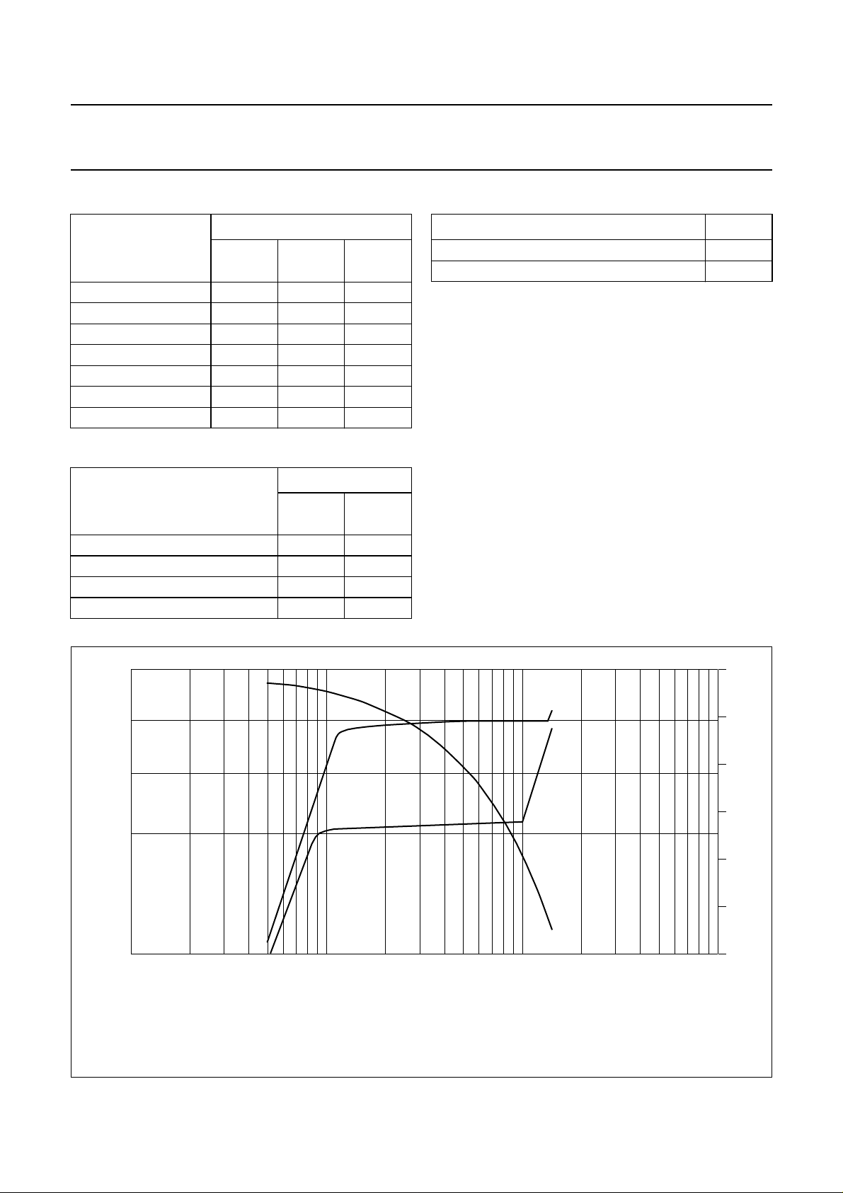
300
handbook, full pagewidth
V
o(rms)
(mV)
250
200
160
100
−2
10
(1) V
CAV
(2) V
o max(rms)
(3) V
o min(rms)
(1)
(2)
(3)
−1
10
AVL measured at pin EOL/EOR.
Y1 axis output level in AVL operation with typically 200 mV.
Y2 axis V
DC voltage at pin CAV corresponds with typical gain steps in range of +6 to −15 dB.
CAV
Fig.4 Automatic volume level control diagram.
MHA312
7
V
CAV
(V)
6
5
4
3
2
1
1
V
I(rms)
(V)
10
1997 Nov 04 32
Page 33

Philips Semiconductors Product specification
I2C-bus controlled BTSC stereo/SAP
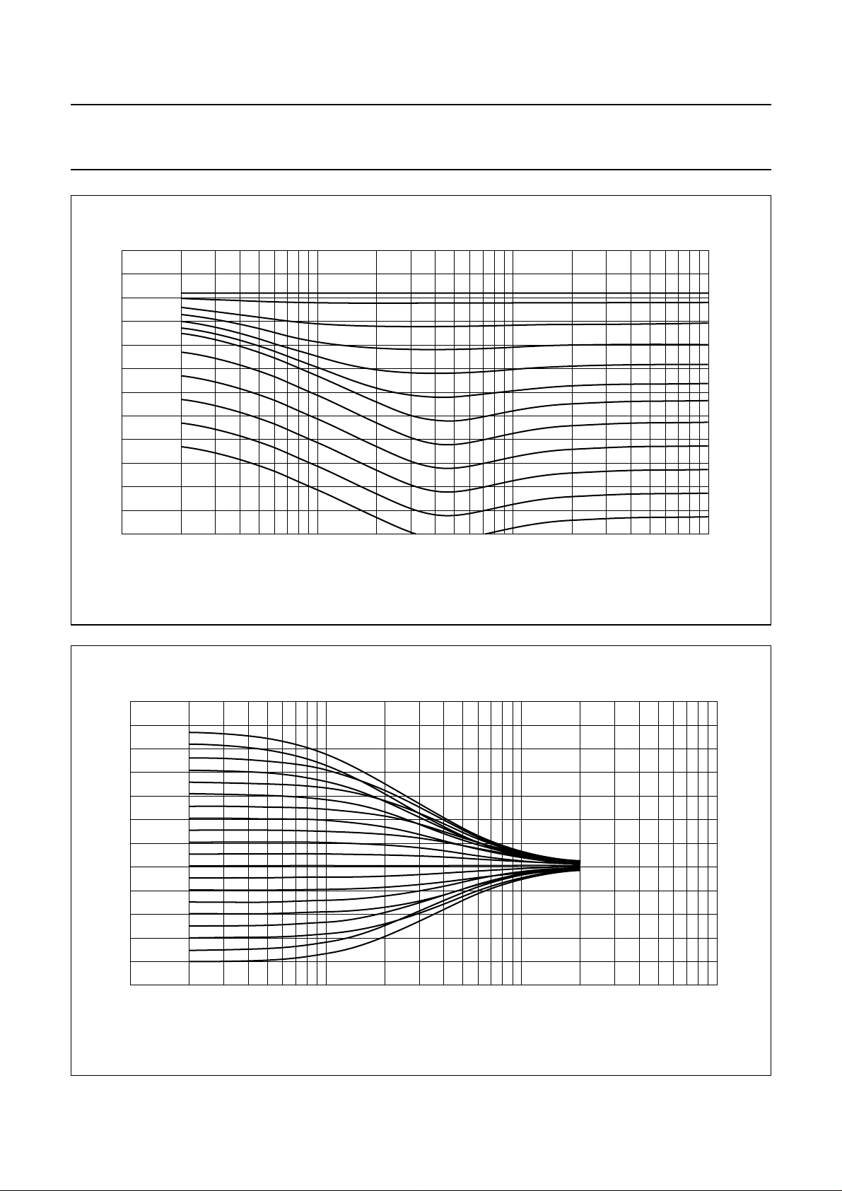
decoder and audio processor
phase
(degree)
−100
−200
−300
−400
0
(1)
(2)
(3)
2
10
10
handbook, full pagewidth
TDA9855
MHA311
3
10
4
10
f (Hz)
5
10
(1) see Table 28.
(2) see Table 28.
(3) see Table 28.
Fig.5 Pseudo (phase in degrees) as a function of frequency (left output).
Table 28 Explanation of curves in Fig.5
CURVE
CAPACITANCE AT PIN C
(nF)
1 15 15 normal
2 5.6 47 intensified
3 5.6 68 more intensified
PS1
CAPACITANCE AT PIN C
(nF)
PS2
EFFECT
1997 Nov 04 33
Page 34
Philips Semiconductors Product specification
I2C-bus controlled BTSC stereo/SAP
decoder and audio processor
25
handbook, full pagewidth
G
c
(dB)
15
5
−5
−15
−25
−35
10 10
20 10
2
TDA9855
MHA844
16
14
9
4
−1
−6
−11
−16
parameter: volume gain setting (dB)
−21
−26
−31
−36
3
f (Hz)
4
10
21
handbook, full pagewidth
18
G
bass
15
(dB)
12
9
6
3
0
−3
−6
−9
−12
−15
10 20 10
Fig.6 Volume control with loudness (including low roll-off frequency).
2
3
10
f (Hz)
MHA843
4
10
Fig.7 Bass control.
1997 Nov 04 34
Page 35

Philips Semiconductors Product specification
I2C-bus controlled BTSC stereo/SAP
decoder and audio processor
15
handbook, full pagewidth
12
G
treble
(dB)
9
6
3
0
−3
−6
−9
−12
−15
2
10
200 10
3
TDA9855
MHA845
4
10
f (Hz)
5
10
60
handbook, halfpage
noise
(µV)
40
20
0
−80
Fig.8 Treble control.
MHA842
−60 20−40 −20 0
gain (dBA)
Fig.9 Noise as function of gain in dBA (RMS value).
1997 Nov 04 35
Page 36
Philips Semiconductors Product specification
I2C-bus controlled BTSC stereo/SAP
decoder and audio processor
handbook, full pagewidth
VI = 200 mV; AVL off
VI = 100 to 1250 mV; AVL on
gain volume = 16 dB (G
LIL
LIR
or
TDA9855
)
v(max)
POWER
STAGE
G = 20 dB
VO = 1.26 V for P
4 dB margin for power peaks
(max)
P
(max)
TDA9855
= 40 W at 4 Ω
MHA841
All values given are in RMS value.
Fig.10 Level diagram.
1997 Nov 04 36
Page 37

Philips Semiconductors Product specification
I2C-bus controlled BTSC stereo/SAP
TDA9855
decoder and audio processor
APPLICATION HINTS
Selection of input signals by using the zero-crossing mute mode (see Fig.11)
A selection between the internal signal path and the external input LIL/LIR produces a modulation click depending on the
difference of the signal values at the time of switching.
At t
the maximum possible difference between signals is 7 V (p-p) and gives a large click. Using the zero-crossing
1
detector no modulation click is audible.
For example: The selection is enabled at t1, the microcontroller sets the zero-crossing bit (TZCM = 1) and then the mute
bit (GMU = 1) via the I2C-bus. The output signal follows the input A signal, until the next zero-crossing occurs and then
activates mute.
After a fixed delay time before t2, the microcontroller has to send the forced mute mode (TZCM = 0) and the return to the
zero-crossing mode (TZCM = 1) to be sure that mute is enabled.
The output signal remains muted until the next signal zero-crossing of input B occurs, and then follows that signal.
The delay time t2− t1 is e.g. 40 ms. The zero-crossing function is working at the lowest frequency of 40 Hz.
handbook, full pagewidth
V
4
3
(1)
MED436
2
1
0
−1
−2
−3
−4
(1) Input A (internal signal).
(2) Output.
(3) Input B (external input signal).
(2)
t
1
t
2
(3)
Fig.11 Zero-crossing function; only one channel shown.
t
1997 Nov 04 37
Page 38

Philips Semiconductors Product specification
I2C-bus controlled BTSC stereo/SAP
decoder and audio processor
Loudness filter calculation example
Figure 12 shows the basic loudness circuit with an
external low-pass filter application. R1 allows an
attenuation range of 21 dB while the boost is determined
by the gain stage V1. Both result in a loudness control
range of +16 to −12 dB.
Defining f
change while switching loudness on/off. The external
resistor R3 for f
=
R3 R1
R3 = 3.2 kΩ is generated.
For the low-pass filter characteristic the value of the
external capacitor C1 can be determined by setting a
specific boost for a defined frequency and referring the
gain to G
1
--------------------j ω C1()
as the frequency where the level does not
ref
→∞ can be calculated as:
ref
G
v
------ 20
10
--------------------110
at f
v
=
. With G
G
v
------ 20
–
as indicated above.
ref
R1 R3+()10
-------------------------------------------------------------110
= −21 dB and R1 = 33 kΩ,
v
G
v
------ 20
R3–×
G
v
------ 20
–
handbook, halfpage
C
KVL
VIX
R3
C1
LOX
R1
33 kΩ
V
Fig.12 Basic loudness circuit.
TDA9855
1
R2
MHA838
For example: 3 dB boost at f = 1 kHz
G
v=Gv(ref)
+ 3 dB = −18 dB; f = 1 kHz and C1 = 100 nF.
If a loudness characteristic with additional high frequency
boost is desired, an additional high-pass section has to be
included in the external filter circuit as indicated in the
block diagram. A filter configuration that provides
AC coupling avoids offset voltage problems.
Figure 13 shows an example of the loudness circuit with
bass and treble boost.
handbook, halfpage
8.2 nF
20 kΩ
220 nF
VIX
LOX
150
nF
2.2 kΩ
R1
33 kΩ
V
1
Fig.13 Loudness circuit with bass and treble boost.
R2
MHA839
1997 Nov 04 38
Page 39
Philips Semiconductors Product specification
I2C-bus controlled BTSC stereo/SAP
decoder and audio processor
handbook, full pagewidth
2 × 220 nF
2 × 600 Ω
V
CC
8.5 V
inputs
4.7
kΩ
12
41
V
P
470
µF
28
TDA9855
100
µF
TDA9855
+8.5 V to
oscilloscope
6
47
301125
100
µF
outputs to
oscilloscope
2 × 4.7 µF
2 × 5 kΩ
MHA840
10
handbook, full pagewidth
(V)
8
6
4
2
0
01234
(1) VCC.
(2) VO.
Fig.14 Turn-on/off power supply circuit diagram.
(1)
(2)
t (s)
MED433
5
Fig.15 Turn-on/off behaviour.
1997 Nov 04 39
Page 40

Philips Semiconductors Product specification
I2C-bus controlled BTSC stereo/SAP
decoder and audio processor
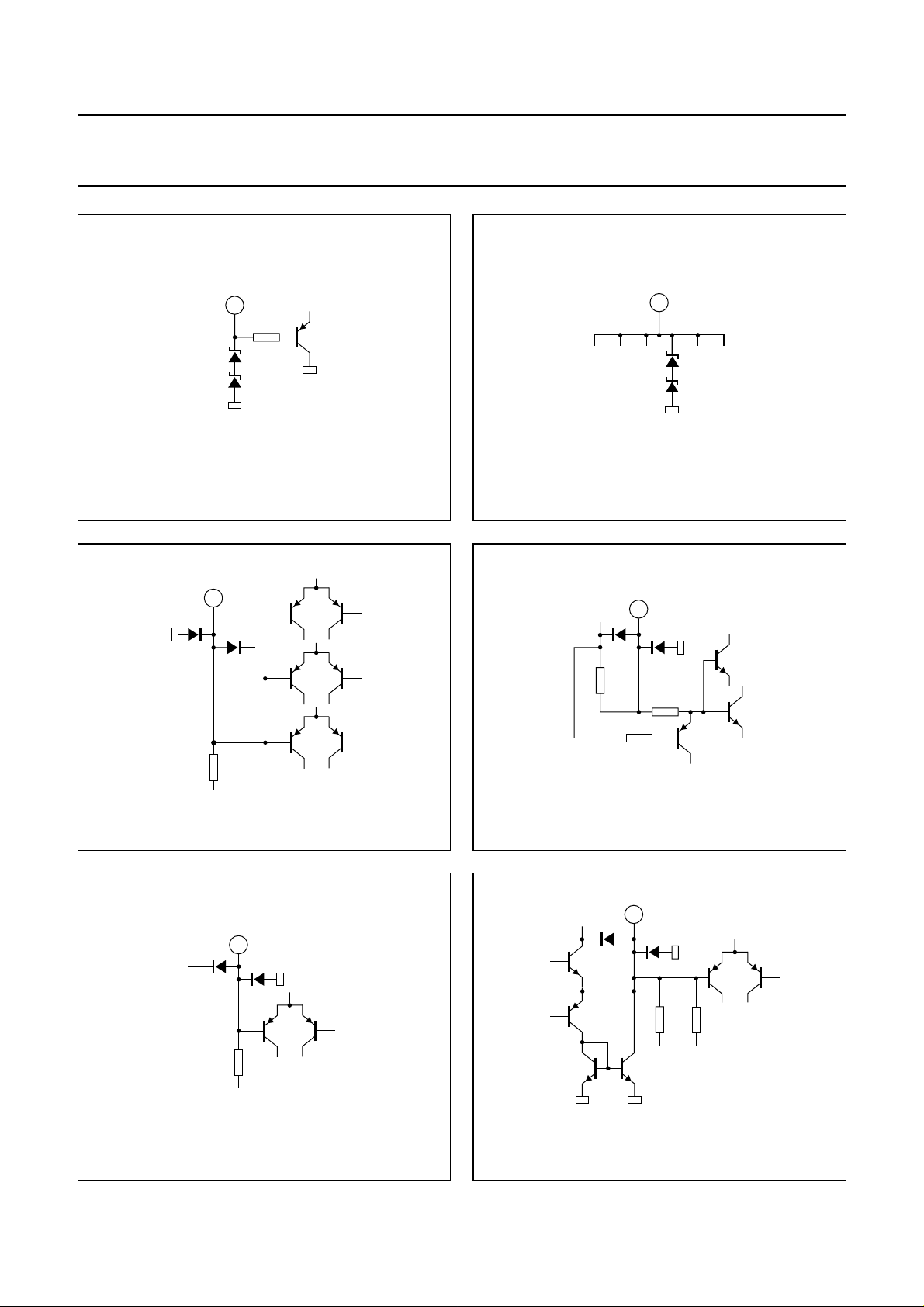
INTERNAL PIN CONFIGURATIONS
The pin numbers refer to the SDIP-version.
handbook, halfpage
4.25 V
1
+
2.4 kΩ
+
MHA846
handbook, halfpage
3.64 kΩ
7.79 kΩ
4.25 V
4.25 V
TDA9855
2
+
MHA847
Fig.16 Pin 1: treble control capacitor, left;
pin 52: treble control capacitor, right.
handbook, halfpage
+
3
4.25 V
80 Ω
MHA848
Fig.18 Pin 3: bass control capacitor output, left;
pin 50: bass control capacitor output, right.
Fig.17 Pin 2: bass control capacitor input, left;
pin 51: bass control capacitor input, right.
handbook, halfpage
+
80 Ω
4
4.25 V
MHA849
Fig.19 Pin 4: output subwoofer;
pin 6: output, left channel;
pin 14: output selector, left channel;
pin 39: output selector, right channel;
pin 47: output, right channel.
1997 Nov 04 40
Page 41
Philips Semiconductors Product specification
I2C-bus controlled BTSC stereo/SAP
decoder and audio processor
handbook, halfpage
+
Fig.20 Pin 5: MAD (I2C-bus address switch).
handbook, halfpage
5
1.8 kΩ
7
TDA9855
MHA850
4.25 V
1.33 kΩ
+
MHA851
Fig.21 Pin 7: input loudness, left; pin 46: input loudness, right.
handbook, halfpage
10.58 kΩ
8
4.25 V
+
4.8 kΩ
Fig.22 Pin 8: input volume, left; pin 45: input volume, right.
1997 Nov 04 41
MHA852
Page 42

Philips Semiconductors Product specification
I2C-bus controlled BTSC stereo/SAP
decoder and audio processor
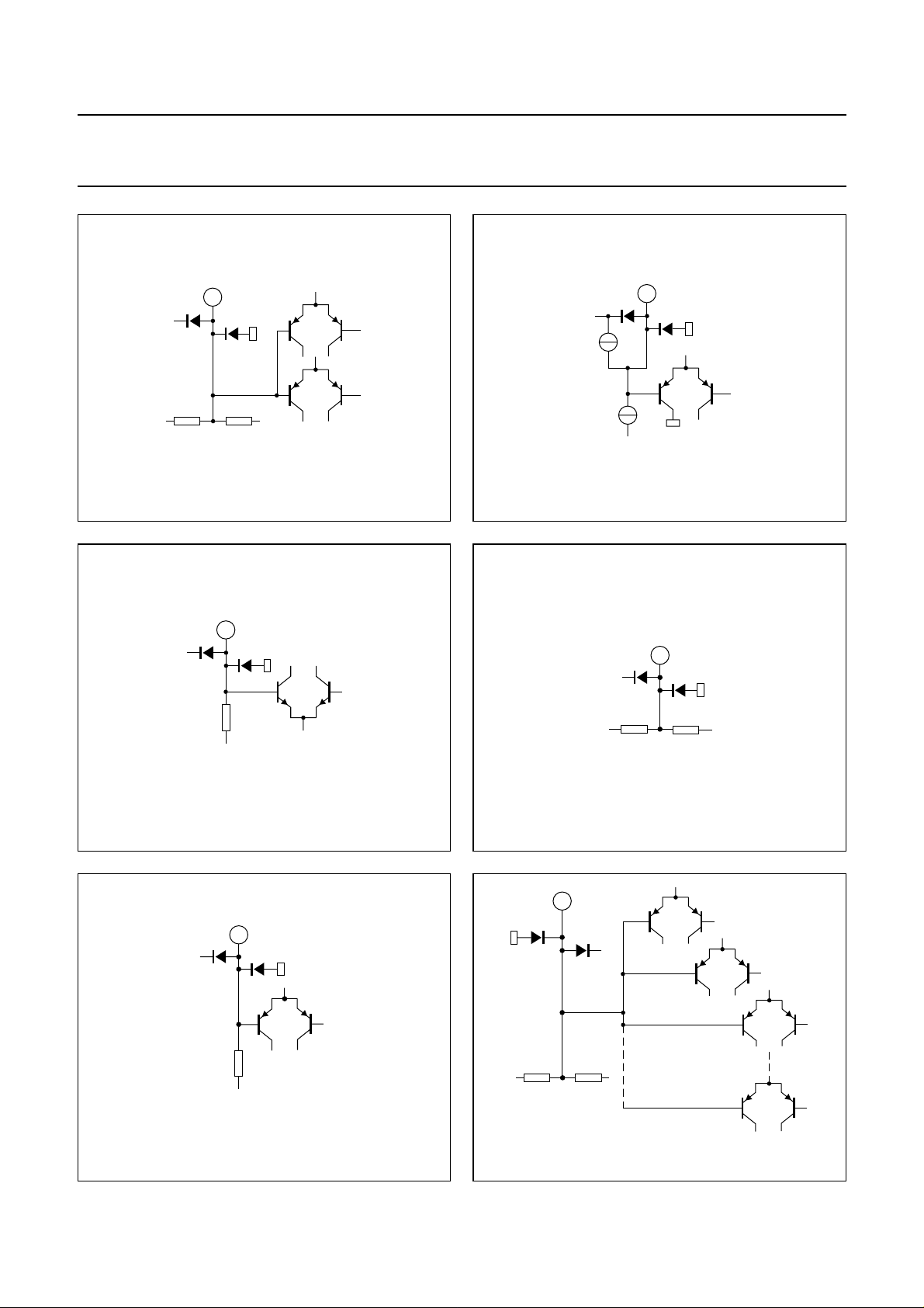
handbook, halfpage
9
+
4.25 V
15kΩ6.8
kΩ
MHA853
handbook, halfpage
TDA9855
10
+
MHA854
handbook, halfpage
Fig.23 Pin 9: output effects, left;
pin 44: output effects, right.
11
+
3.4 kΩ
3.4 kΩ
MHA855
Fig.24 Pin 10: automatic volume control capacitor.
handbook, halfpage
12
+
20 kΩ 20 kΩ
4.25 V
MHA856
Fig.25 Pin 11: reference voltage 0.5VCC.
1997 Nov 04 42
Fig.26 Pin 12: line input, left;
pin 41: line input, right.
Page 43
Philips Semiconductors Product specification
I2C-bus controlled BTSC stereo/SAP
decoder and audio processor
handbook, halfpage
13
4.25 V
1
+
2
3
1.75 kΩ
8
MHA857
handbook, halfpage
TDA9855
4.25 V
15
+
5 kΩ
MHA858
Fig.27 Pin 13: input automatic volume control, left;
pin 40: input automatic volume control, right.
handbook, halfpage
+
16
MHA859
handbook, halfpage
Fig.28 Pin 15: line output, left;
pin 38: line output, right.
18
+
4.25 V
6 kΩ
MHA860
Fig.29 Pin 16: timing capacitor wideband for dbx;
pin 17: timing capacitor spectral for dbx.
1997 Nov 04 43
Fig.30 Pin 18: capacitor wideband for dbx;
pin 19: capacitor spectral for dbx.
Page 44

Philips Semiconductors Product specification
I2C-bus controlled BTSC stereo/SAP
decoder and audio processor
handbook, halfpage
Fig.31 Pin 20: variable emphasis out for dbx.
20
+
MHA861
handbook, halfpage
21
+
600 Ω
MHA862
Fig.32 Pin 21: variable emphasis in for dbx.
TDA9855
handbook, halfpage
+
10 kΩ
22
4.25 V
MHA863
Fig.33 Pin 22: capacitor noise reduction for dbx.
handbook, halfpage
24
+
4.25 V
handbook, halfpage
Fig.34 Pin 23: capacitor mute for SAP.
handbook, halfpage
23
+
MHA864
26
5 V
1.8 kΩ
20 kΩ 20 kΩ
MHA865
Fig.35 Pin 24: capacitor DC decoupling for SAP.
1997 Nov 04 44
MHA866
Fig.36 Pin 26: SDA (I2C-bus data input/output).
Page 45
Philips Semiconductors Product specification
I2C-bus controlled BTSC stereo/SAP
decoder and audio processor
handbook, halfpage
Fig.37 Pin 27: SCL (I2C-bus clock).
handbook, halfpage
5 V
29
27
1.8 kΩ
MHA867
4.25 V
+
handbook, halfpage
handbook, halfpage
TDA9855
apply 8.5 V to this pin
28
MHA868
Fig.38 Pin 28: supply voltage.
30
+
Fig.39 Pin 29: input composite signal.
handbook, halfpage
+
3.5 kΩ
30 kΩ
31
4.25 V
MHA869
MHA871
4.7
kΩ
300 Ω
5 kΩ
MHA870
Fig.40 Pin 30: smoothing capacitor for supply.
handbook, halfpage
+
32
4.25 V
3.5
kΩ
3.5
kΩ
MHA872
Fig.41 Pin 31: capacitor for pilot detector.
1997 Nov 04 45
Fig.42 Pin 32: capacitor for pilot detector.
Page 46
Philips Semiconductors Product specification
I2C-bus controlled BTSC stereo/SAP
decoder and audio processor
handbook, halfpage
+
10 kΩ 10 kΩ
Fig.43 Pin 33: capacitor for phase detector.
33
4.25 V
MHA873
handbook, halfpage
Fig.44 Pin 34: capacitor for filter adjust.
TDA9855
34
+
MHA874
handbook, halfpage
handbook, halfpage
35
+
3 kΩ
MHA875
Fig.45 Pin 35: ceramic resonator.
43
+
4.25 V
15 kΩ
MHA877
handbook, halfpage
36
+
10 kΩ 10 kΩ
4.25 V
MHA876
Fig.46 Pin 36: capacitor DC decoupling mono;
pin 37: capacitor DC decoupling stereo/SAP.
handbook, halfpage
4.25 V
10 kΩ
49
10 kΩ
+
1
2
3
Fig.47 Pin 43: capacitor 1 pseudo function;
pin 42: capacitor 2 pseudo function.
1997 Nov 04 46
Fig.48 Pin 49: capacitor subwoofer.
8
MHA878
Page 47

Philips Semiconductors Product specification
I2C-bus controlled BTSC stereo/SAP
decoder and audio processor
PACKAGE OUTLINES
SDIP52: plastic shrink dual in-line package; 52 leads (600 mil)
D
seating plane
L
Z
e
TDA9855
SOT247-1
M
E
A
2
A
A
1
w M
b
1
c
(e )
M
1
H
52
pin 1 index
1
DIMENSIONS (mm are the original dimensions)
A
A
A
UNIT b
max.
mm
5.08 0.51 4.0
12
min.
max.
b
1.3
0.8
0.53
0.40
b
27
E
26
0 5 10 mm
scale
cEe M
1
0.32
0.23
(1) (1)
D
47.9
47.1
14.0
13.7
1
L
M
E
3.2
15.80
2.8
15.24
17.15
15.90
e
w
H
0.181.778 15.24
Z
max.
1.73
(1)
Note
1. Plastic or metal protrusions of 0.25 mm maximum per side are not included.
OUTLINE
VERSION
SOT247-1
IEC JEDEC EIAJ
REFERENCES
1997 Nov 04 47
EUROPEAN
PROJECTION
ISSUE DATE
90-01-22
95-03-11
Page 48
Philips Semiconductors Product specification
I2C-bus controlled BTSC stereo/SAP
decoder and audio processor
PLCC68: plastic leaded chip carrier; 68 leads
e
y
61
68
1
pin 1 index
D
X
4460
TDA9855
SOT188-2
e
E
A
Z
E
43
b
p
b
1
w M
H
E
E
e
A
A
1
A
4
(A )
3
k
9
β
1
27
k
10 26
e
Z
D
H
D
D
v M
A
B
v M
B
0 5 10 mm
scale
DIMENSIONS (millimetre dimensions are derived from the original inch dimensions)
UNIT A
mm
inches
A
1
min. max. max. max. max.
4.57
0.51
4.19
0.180
0.020
0.165
A
0.25
0.01
A
4
3
3.30
0.13
b
0.53
0.33
0.021
0.013
b
p
1
0.81
0.66
0.032
0.026
D
24.33
24.13
0.958
0.950
(1)
(1)
E
eH
e
D
1.27
0.05
23.62
22.61
0.930
0.890
24.33
24.13
0.958
0.950
e
E
23.62
22.61
0.930
0.890
H
25.27
25.02
0.995
0.985
D
25.27
25.02
0.995
0.985
Note
1. Plastic or metal protrusions of 0.01 inches maximum per side are not included.
OUTLINE
VERSION
SOT188-2
IEC JEDEC EIAJ
112E10 MO-047AC
REFERENCES
k
1
k
E
1.22
1.07
0.048
0.042
0.51
0.020
L
1.44
1.02
0.057
0.040
detail X
p
0.007 0.0040.007
EUROPEAN
PROJECTION
L
p
(1) (1)
Z
Z
E
D
ywv β
0.18 0.100.18
2.16
0.085
2.16
0.085
o
45
ISSUE DATE
92-11-17
95-03-11
1997 Nov 04 48
Page 49

Philips Semiconductors Product specification
I2C-bus controlled BTSC stereo/SAP
decoder and audio processor
SOLDERING
Introduction
There is no soldering method that is ideal for all IC
packages. Wave soldering is often preferred when
through-hole and surface mounted components are mixed
on one printed-circuit board. However, wave soldering is
not always suitable for surface mounted ICs, or for
printed-circuits with high population densities. In these
situations reflow soldering is often used.
This text gives a very brief insight to a complex technology.
A more in-depth account of soldering ICs can be found in
our
“IC Package Databook”
SDIP
SOLDERING BY DIPPING OR BY WA VE
The maximum permissible temperature of the solder is
260 °C; solder at this temperature must not be in contact
with the joint for more than 5 seconds. The total contact
time of successive solder waves must not exceed
5 seconds.
The device may be mounted up to the seating plane, but
the temperature of the plastic body must not exceed the
specified maximum storage temperature (T
printed-circuit board has been pre-heated, forced cooling
may be necessary immediately after soldering to keep the
temperature within the permissible limit.
R
EPAIRING SOLDERED JOINTS
Apply a low voltage soldering iron (less than 24 V) to the
lead(s) of the package, below the seating plane or not
more than 2 mm above it. If the temperature of the
soldering iron bit is less than 300 °C it may remain in
contact for up to 10 seconds. If the bit temperature is
between 300 and 400 °C, contact may be up to 5 seconds.
(order code 9398 652 90011).
). If the
stg max
TDA9855
Reflow soldering requires solder paste (a suspension of
fine solder particles, flux and binding agent) to be applied
to the printed-circuit board by screen printing, stencilling or
pressure-syringe dispensing before package placement.
Several techniques exist for reflowing; for example,
thermal conduction by heated belt. Dwell times vary
between 50 and 300 seconds depending on heating
method. Typical reflow temperatures range from
215 to 250 °C.
Preheating is necessary to dry the paste and evaporate
the binding agent. Preheating duration: 45 minutes at
45 °C.
WAVE SOLDERING
Wave soldering techniques can be used for all PLCC
packages if the following conditions are observed:
• A double-wave (a turbulent wave with high upward
pressure followed by a smooth laminar wave) soldering
technique should be used.
• The longitudinal axis of the package footprint must be
parallel to the solder flow.
• The package footprint must incorporate solder thieves at
the downstream corners.
During placement and before soldering, the package must
be fixed with a droplet of adhesive. The adhesive can be
applied by screen printing, pin transfer or syringe
dispensing. The package can be soldered after the
adhesive is cured.
Maximum permissible solder temperature is 260 °C, and
maximum duration of package immersion in solder is
10 seconds, if cooled to less than 150 °C within
6 seconds. Typical dwell time is 4 seconds at 250 °C.
A mildly-activated flux will eliminate the need for removal
of corrosive residues in most applications.
PLCC
REFLOW SOLDERING
Reflow soldering techniques are suitable for all PLCC
packages.
The choice of heating method may be influenced by larger
PLCC packages (44 leads, or more). If infrared or vapour
phase heating is used and the large packages are not
absolutely dry (less than 0.1% moisture content by
weight), vaporization of the small amount of moisture in
them can cause cracking of the plastic body. For more
information, refer to the Drypack chapter in our
Reference Handbook”
1997 Nov 04 49
(order code 9398 510 63011).
“Quality
EPAIRING SOLDERED JOINTS
R
Fix the component by first soldering two diagonally-
opposite end leads. Use only a low voltage soldering iron
(less than 24 V) applied to the flat part of the lead. Contact
time must be limited to 10 seconds at up to 300 °C. When
using a dedicated tool, all other leads can be soldered in
one operation within 2 to 5 seconds between
270 and 320 °C.
Page 50
Philips Semiconductors Product specification
I2C-bus controlled BTSC stereo/SAP
TDA9855
decoder and audio processor
DEFINITIONS
Data sheet status
Objective specification This data sheet contains target or goal specifications for product development.
Preliminary specification This data sheet contains preliminary data; supplementary data may be published later.
Product specification This data sheet contains final product specifications.
Limiting values
Limiting values given are in accordance with the Absolute Maximum Rating System (IEC 134). Stress above one or
more of the limiting values may cause permanent damage to the device. These are stress ratings only and operation
of the device at these or at any other conditions above those given in the Characteristics sections of the specification
is not implied. Exposure to limiting values for extended periods may affect device reliability.
Application information
Where application information is given, it is advisory and does not form part of the specification.
LIFE SUPPORT APPLICATIONS
These products are not designed for use in life support appliances, devices, or systems where malfunction of these
products can reasonably be expected to result in personal injury. Philips customers using or selling these products for
use in such applications do so at their own risk and agree to fully indemnify Philips for any damages resulting from such
improper use or sale.
PURCHASE OF PHILIPS I
Purchase of Philips I
components in the I2C system provided the system conforms to the I2C specification defined by
Philips. This specification can be ordered using the code 9398 393 40011.
2
C COMPONENTS
2
C components conveys a license under the Philips’ I2C patent to use the
1997 Nov 04 50
Page 51

Philips Semiconductors Product specification
I2C-bus controlled BTSC stereo/SAP
decoder and audio processor
NOTES
TDA9855
1997 Nov 04 51
Page 52

Philips Semiconductors – a worldwide company
Argentina: see South America
Australia: 34 Waterloo Road, NORTH RYDE, NSW 2113,
Tel. +61 2 9805 4455, Fax. +61 2 9805 4466
Austria: Computerstr. 6, A-1101 WIEN, P.O. Box 213, Tel. +43 160 1010,
Fax. +43 160 101 1210
Belarus: Hotel Minsk Business Center, Bld. 3, r. 1211, Volodarski Str. 6,
220050 MINSK, Tel. +375 172 200 733, Fax. +375 172 200 773
Belgium: see The Netherlands
Brazil: see South America
Bulgaria: Philips Bulgaria Ltd., Energoproject, 15th floor,
51 James Bourchier Blvd., 1407 SOFIA,
Tel. +359 2 689 211, Fax. +359 2 689 102
Canada: PHILIPS SEMICONDUCTORS/COMPONENTS,
Tel. +1 800 234 7381
China/Hong Kong: 501 Hong Kong Industrial Technology Centre,
72 Tat Chee Avenue, Kowloon Tong, HONG KONG,
Tel. +852 2319 7888, Fax. +852 2319 7700
Colombia: see South America
Czech Republic: see Austria
Denmark: Prags Boulevard 80, PB 1919, DK-2300 COPENHAGEN S,
Tel. +45 32 88 2636, Fax. +45 31 57 0044
Finland: Sinikalliontie 3, FIN-02630 ESPOO,
Tel. +358 9 615800, Fax. +358 9 61580920
France: 4 Rue du Port-aux-Vins, BP317, 92156 SURESNES Cedex,
Tel. +33 1 40 99 6161, Fax. +33 1 40 99 6427
Germany: Hammerbrookstraße 69, D-20097 HAMBURG,
Tel. +49 40 23 53 60, Fax. +49 40 23 536 300
Greece: No. 15, 25th March Street, GR 17778 TAVROS/ATHENS,
Tel. +30 1 4894 339/239, Fax. +30 1 4814 240
Hungary: see Austria
India: Philips INDIA Ltd, Band Box Building, 2nd floor,
254-D, Dr. Annie Besant Road, Worli, MUMBAI 400 025,
Tel. +91 22 493 8541, Fax. +91 22 493 0966
Indonesia: see Singapore
Ireland: Newstead, Clonskeagh, DUBLIN 14,
Tel. +353 1 7640 000, Fax. +353 1 7640 200
Israel: RAPAC Electronics, 7 Kehilat Saloniki St, PO Box 18053,
TEL AVIV 61180, Tel. +972 3 645 0444, Fax. +972 3 649 1007
Italy: PHILIPS SEMICONDUCTORS, Piazza IV Novembre 3,
20124 MILANO, Tel. +39 2 6752 2531, Fax. +39 2 6752 2557
Japan: Philips Bldg 13-37, Kohnan 2-chome, Minato-ku, TOKYO 108,
Tel. +81 3 3740 5130, Fax. +81 3 3740 5077
Korea: Philips House, 260-199 Itaewon-dong, Yongsan-ku, SEOUL,
Tel. +82 2 709 1412, Fax. +82 2 709 1415
Malaysia: No. 76 Jalan Universiti, 46200 PETALING JAYA, SELANGOR,
Tel. +60 3 750 5214, Fax. +60 3 757 4880
Mexico: 5900 Gateway East, Suite 200, EL PASO, TEXAS 79905,
Tel. +9-5 800 234 7381
Middle East: see Italy
Netherlands: Postbus 90050, 5600 PB EINDHOVEN, Bldg. VB,
Tel. +31 40 27 82785, Fax. +31 40 27 88399
New Zealand: 2 Wagener Place, C.P.O. Box 1041, AUCKLAND,
Tel. +64 9 849 4160, Fax. +64 9 849 7811
Norway: Box 1, Manglerud 0612, OSLO,
Tel. +47 22 74 8000, Fax. +47 22 74 8341
Philippines: Philips Semiconductors Philippines Inc.,
106 Valero St. Salcedo Village, P.O. Box 2108 MCC, MAKATI,
Metro MANILA, Tel. +63 2 816 6380, Fax. +63 2 817 3474
Poland: Ul. Lukiska 10, PL 04-123 WARSZAWA,
Tel. +48 22 612 2831, Fax. +48 22 612 2327
Portugal: see Spain
Romania: see Italy
Russia: Philips Russia, Ul. Usatcheva 35A, 119048 MOSCOW,
Tel. +7 095 755 6918, Fax. +7 095 755 6919
Singapore: Lorong 1, Toa Payoh, SINGAPORE 1231,
Tel. +65 350 2538, Fax. +65 251 6500
Slovakia: see Austria
Slovenia: see Italy
South Africa: S.A. PHILIPS Pty Ltd., 195-215 Main Road Martindale,
2092 JOHANNESBURG, P.O. Box 7430 Johannesburg 2000,
Tel. +27 11 470 5911, Fax. +27 11 470 5494
South America: Rua do Rocio 220, 5th floor, Suite 51,
04552-903 São Paulo, SÃO PAULO - SP, Brazil,
Tel. +55 11 821 2333, Fax. +55 11 829 1849
Spain: Balmes 22, 08007 BARCELONA,
Tel. +34 3 301 6312, Fax. +34 3 301 4107
Sweden: Kottbygatan 7, Akalla, S-16485 STOCKHOLM,
Tel. +46 8 632 2000, Fax. +46 8 632 2745
Switzerland: Allmendstrasse 140, CH-8027 ZÜRICH,
Tel. +41 1 488 2686, Fax. +41 1 481 7730
Taiwan: Philips Semiconductors, 6F, No. 96, Chien Kuo N. Rd., Sec. 1,
TAIPEI, Taiwan Tel. +886 2 2134 2865, Fax. +886 2 2134 2874
Thailand: PHILIPS ELECTRONICS (THAILAND) Ltd.,
209/2 Sanpavuth-Bangna Road Prakanong, BANGKOK 10260,
Tel. +66 2 745 4090, Fax. +66 2 398 0793
Turkey: Talatpasa Cad. No. 5, 80640 GÜLTEPE/ISTANBUL,
Tel. +90 212 279 2770, Fax. +90 212 282 6707
Ukraine: PHILIPS UKRAINE, 4 Patrice Lumumba str., Building B, Floor 7,
252042 KIEV, Tel. +380 44 264 2776, Fax. +380 44 268 0461
United Kingdom: Philips Semiconductors Ltd., 276 Bath Road, Hayes,
MIDDLESEX UB3 5BX, Tel. +44 181 730 5000, Fax. +44 181 754 8421
United States: 811 East Arques Avenue, SUNNYVALE, CA 94088-3409,
Tel. +1 800 234 7381
Uruguay: see South America
Vietnam: see Singapore
Yugoslavia: PHILIPS, Trg N. Pasica 5/v, 11000 BEOGRAD,
Tel. +381 11 625 344, Fax.+381 11 635 777
For all other countries apply to: Philips Semiconductors, Marketing & Sales Communications,
Building BE-p, P.O. Box 218, 5600 MD EINDHOVEN, The Netherlands, Fax. +31 40 27 24825
© Philips Electronics N.V. 1997 SCA55
All rights are reserved. Reproduction in whole or in part is prohibited without the prior written consent of the copyright owner.
The information presented in this document does not form part of any quotation or contract, is believed to be accurate and reliable and may be changed
without notice. No liability will be accepted by the publisher for any consequence of its use. Publication thereof does not convey nor imply any license
under patent- or other industrial or intellectual property rights.
Internet: http://www.semiconductors.philips.com
Printed in The Netherlands 547047/1200/03/pp52 Date of release: 1997Nov 04 Document order number: 9397 750 02446
 Loading...