

Page 1
INTEGRATED CIRCUITS
DATA SH EET
TDA9852
2
I
C-bus controlled BTSC
stereo/SAP decoder and audio
processor
Preliminary specification
File under Integrated Circuits, IC02
1996 Feb 28
Page 2

Philips Semiconductors Preliminary specification
I2C-bus controlled BTSC stereo/SAP
decoder and audio processor
FEATURES
• Quasi alignment-free application due to automatic
adjustment of channel separation via I2C-bus
• High integration level with automatically tuned
integrated filters
• Input level adjustment I2C-bus controlled
• Alignment-free SAP processing
• dbx noise reduction circuit
• Power supply
• I2C-bus transceiver.
Stereo decoder
• Stereo pilot PLL circuit with ceramic resonator,
automatic adjustment procedure for stereo channel
separation, two pilot thresholds selectable via I
Audio processor
2
C-bus.
TDA9852
GENERAL DESCRIPTION
The TDA9852 is a bipolar-integrated BTSC stereo
decoder with hi-fi audio processor (I
application in TV sets, VCRs and multimedia.
2
C-bus controlled) for
• Selector for internal and external signals (line in)
• Automatic volume level control
(control range +6 to −15 dB)
• Interface for external noise reduction circuits
• Volume control (control range +16 to −71 dB)
• Special loudness characteristic automatically controlled
in combination with volume setting (control range 28 dB)
• Audio signal zero crossing detection between any
volume step switching
• Mute control at audio signal zero crossing
2
• Mute control via I
ORDERING INFORMATION
TYPE NUMBER
TDA9852 SDIP42 plastic shrink dual in-line package; 42 leads (600 mil) SOT270-1
C-bus.
PACKAGE
NAME DESCRIPTION VERSION
1996 Feb 28 2
Page 3
Philips Semiconductors Preliminary specification
I2C-bus controlled BTSC stereo/SAP
TDA9852
decoder and audio processor
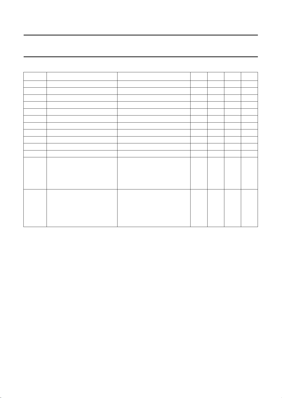
QUICK REFERENCE DATA
SYMBOL PARAMETER CONDITIONS MIN. TYP. MAX. UNIT
V
CC
I
CC
V
comp(rms)
V
oR,L(rms)
G
LA
α
cs
THD
V
I, O(rms)
AVL control range −15 − +6 dB
G
C
L
B
S/N signal-to-noise ratio line out (mono); V
S/N signal-to-noise ratio audio section; V
supply voltage 8.0 8.5 9.0 V
supply current − 75 95 mA
input signal voltage (RMS value) 100% modulation L + R; fi= 300 Hz − 250 − mV
output signal voltage (RMS value) 100% modulation L + R; fi= 300 Hz − 500 − mV
input level adjustment control −3.5 − +4.0 dB
stereo channel separation fL= 300 Hz; fR= 3 kHz 25 35 − dB
total harmonic distortion L + R fi= 1 kHz − 0.2 − %
L,R
signal handling (RMS value) THD < 0.5% 2 −−V
volume control range −71 − +16 dB
maximum loudness boost fi=40Hz − 17 − dB
= 0.5 V (RMS)
o
CCIR noise weighting filter
− 60 − dB
(peak value)
DIN noise weighting filter
− 73 − dBA
(RMS value)
= 2 V (RMS);
o
gain = 0 dB
CCIR noise weighting filter
− 94 − dB
(peak value)
DIN noise weighting filter
− 107 − dBA
(RMS value)
1996 Feb 28 3
Page 4
Philips Semiconductors Preliminary specification
I2C-bus controlled BTSC stereo/SAP
decoder and audio processor
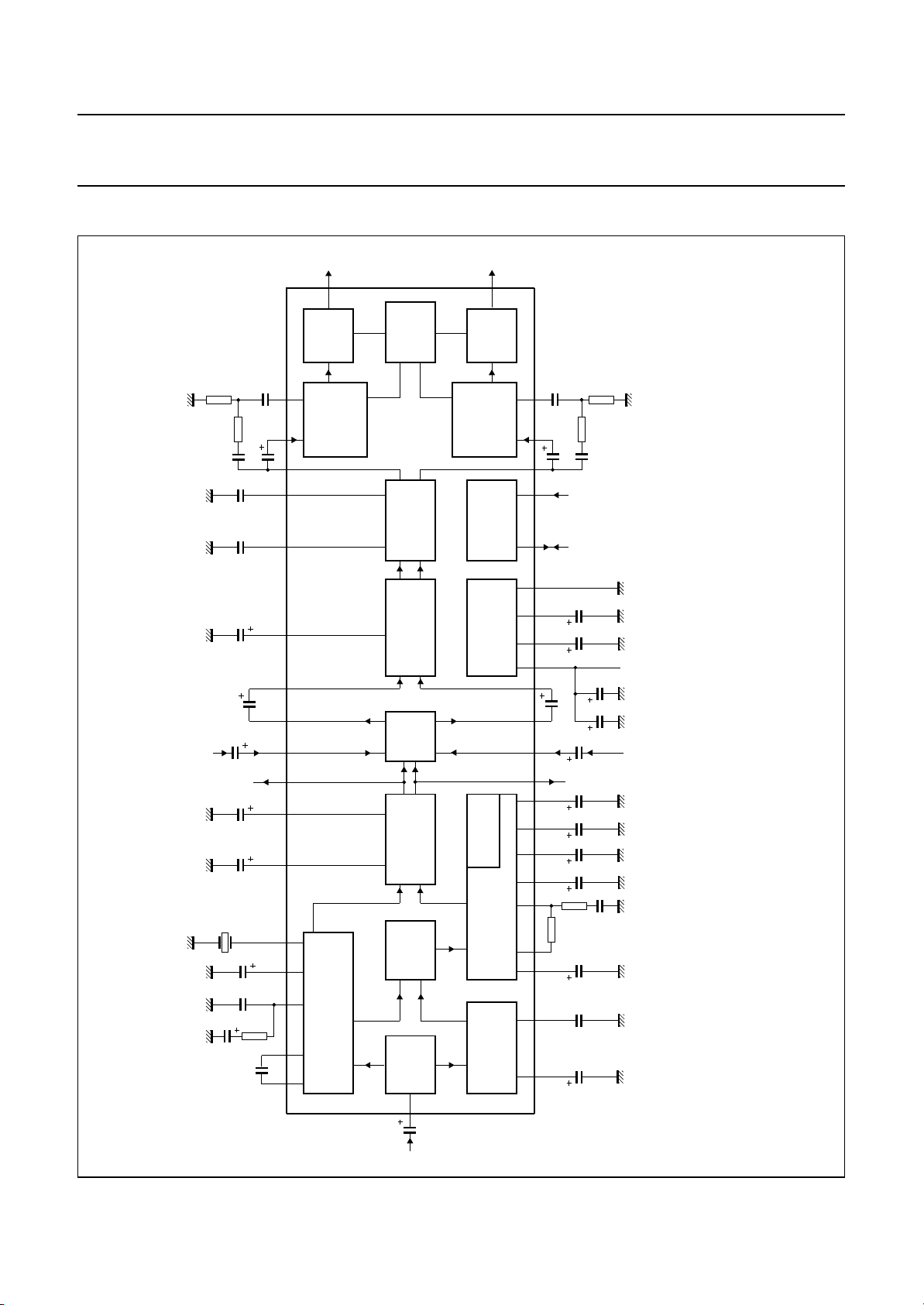
BLOCK DIAGRAM
OUTR
42
OUT
RIGHT
C12
R3
R2
C11
C9
C8C28
C10
VIR
41
4039
38375
RIGHT
VOLUME
LOUDNESS
CONTROL
ZERO
CROSSING
EFFECTS
OUTL
1
OUT
LEFT
LEFT
VOLUME
LOUDNESS
C
2
I
LOGIC
MHA309
C14
34212068972523
VIL
CONTROL
22 2
TRANSCEIVER
C29
TDA9852
R5
R4
C30
SDA SCL
C6
C7
(EIR)
External Input Right
C20
C16
Q1
CERAMIC
C5
C4
C3
C2
RESONATOR
MURATA
R1
LIR
LOR
32 33 36 34 35
31
CSB503F58
26 27 28 29 30
TDA9852
AUTOMATIC
VOLUME AND
INPUT
+
DEMATRIX
SAP
STEREO/
STEREO DECODER
INPUT
24
COMP
LEVEL
LEVEL CONTROL
SELECT
SELECT
LINEOUT
SWITCH
ADJUST
C1
STEREO
SUPPLY
LIL
LOL
11 1012
ADJUST
1314
DBX
SAP
R6
15 16
171819
DEMODULATOR
C26
C27
R7
C19
C18C17
C34
C15
C49
C47
C25
C24
C23
C22
C21
CC
V
(EIL)
External Input Left
handbook, full pagewidth
Fig.1 Block diagram.
1996 Feb 28 4
Page 5
Philips Semiconductors Preliminary specification
I2C-bus controlled BTSC stereo/SAP
TDA9852
decoder and audio processor
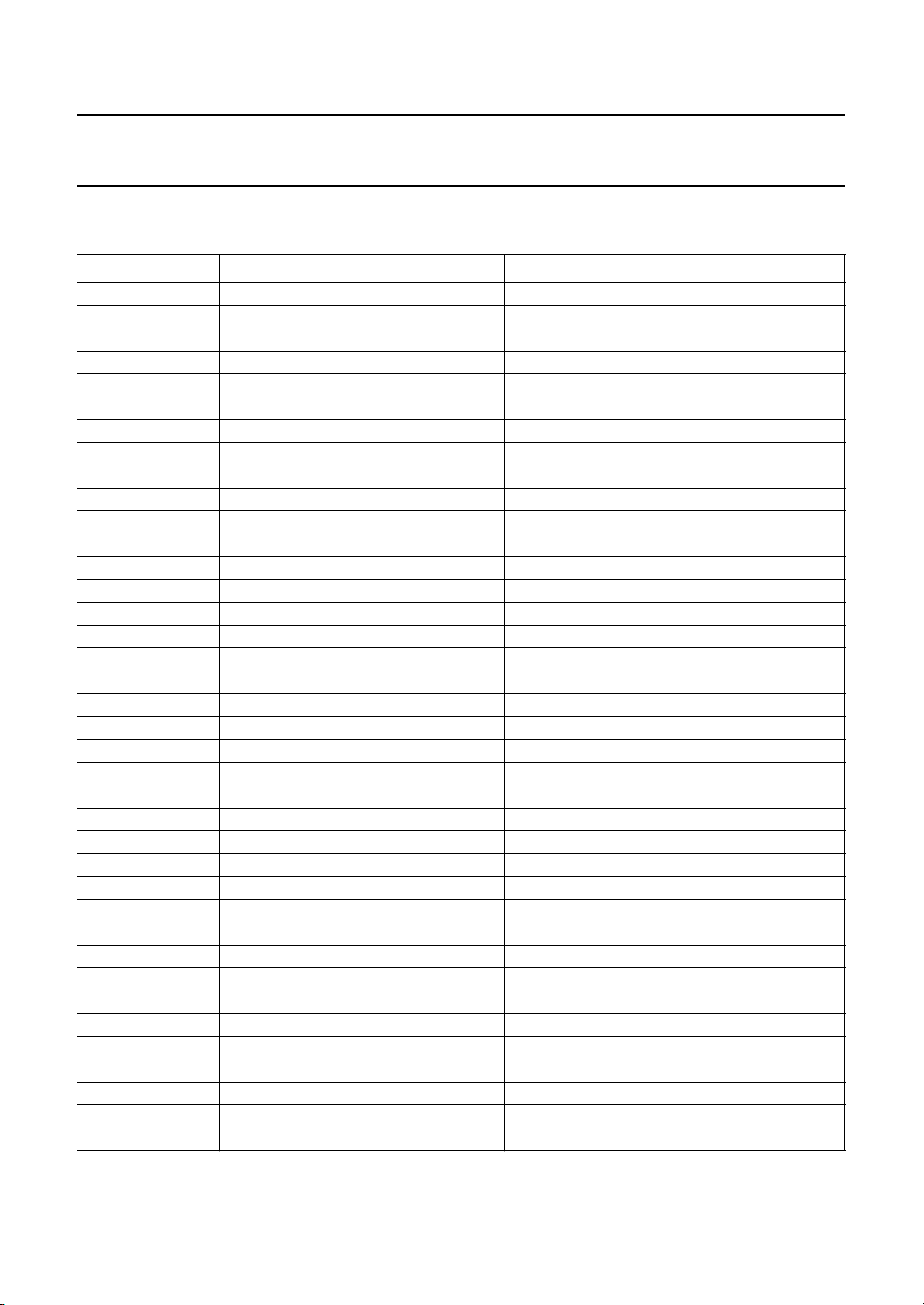
Component list
Electrolytic capacitors ±20%; foil or ceramic capacitors ±10%; resistors ±5%; unless otherwise specified; see Fig.1.
COMPONENT VALUE TYPE REMARK
C1 10 µF electrolytic 63 V
C2 470 nF foil
C3 4.7 µF electrolytic 63 V
C4 220 nF foil
C5 10 µF electrolytic 63 V; I
C6 2.2 µF electrolytic 16 V
C7 2.2 µF electrolytic 63 V
C8 15 nF foil ±5%
C9 15 nF foil ±5%
C10 2.2 µF electrolytic 16 V
C11 8.2 nF foil or ceramic ±5% SMD 2220/1206
C12 150 nF foil ±5%
C14 150 nF foil ±5%
C15 100 µF electrolytic 16 V
C16 4.7 µF electrolytic 63 V
C17 4.7 µF electrolytic 63 V
C18 100 nF foil
C19 10 µF electrolytic 63 V
C20 4.7 µF electrolytic 63 V
C21 47 nF foil ±5%
C22 1 µF electrolytic 63 V
C23 1 µF electrolytic 63 V
C24 10 µF electrolytic 63 V ±10%
C25 10 µF electrolytic 63 V ±10%
C26 2.2 µF electrolytic 16 V
C27 2.2 µF electrolytic 63 V
C28 4.7 µF electrolytic 63 V ±10%
C29 2.2 µF electrolytic 16 V
C30 8.2 nF foil or ceramic ±5% SMD 2220/1206
C34 100 µF electrolytic 16 V
C47 220 µF electrolytic 25 V
C49 100 nF foil or ceramic SMD 1206
R1 2.2 kΩ−
R2 20 kΩ−
R3 2.2 kΩ−
R4 20 kΩ−
R5 2.2 kΩ−
R6 8.2 kΩ− ±2%
leak
< 1.5 µA
1996 Feb 28 5
Page 6
Philips Semiconductors Preliminary specification
I2C-bus controlled BTSC stereo/SAP
decoder and audio processor
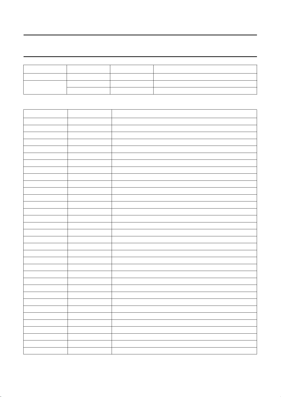
COMPONENT VALUE TYPE REMARK
R7 160 Ω− ±2%
Q1 CSB503F58 radial leads
CSB503JF958 alternative as SMD
PINNING
SYMBOL PIN DESCRIPTION
OUTL 1 output, left channel
LDL 2 input loudness, left channel
VIL 3 input volume, left channel
EOL 4 output effects, left channel
C
AV
V
ref
LIL 7 input line control, left channel
AVL 8 input automatic volume control, left channel
SOL 9 output selector, left channel
LOL 10 output line control, left channel
C
TW
C
TS
C
W
C
S
VEO 15 variable emphasis output for dbx
VEI 16 variable emphasis input for dbx
C
NR
C
M
C
DEC
GND 20 ground
SDA 21 serial data input/output
SCL 22 serial clock input
V
CC
COMP 24 composite input signal
V
CAP
C
P1
C
P2
C
PH
C
ADJ
CER 30 ceramic resonator
C
MO
C
SS
LOR 33 output line control, right channel
SOR 34 output selector, right channel
5 automatic volume control capacitor
6 reference voltage 0.5V
CC
11 capacitor timing wideband for dbx
12 capacitor timing spectral for dbx
13 capacitor wideband for dbx
14 capacitor spectral for dbx
17 capacitor noise reduction for dbx
18 capacitor mute for SAP
19 capacitor DC-decoupling for SAP
23 supply voltage
25 capacitor for electronic filtering of supply
26 capacitor for pilot detector
27 capacitor for pilot detector
28 capacitor for phase detector
29 capacitor for filter adjustment
31 capacitor DC-decoupling mono
32 capacitor DC-decoupling stereo/SAP
TDA9852
1996 Feb 28 6
Page 7
Philips Semiconductors Preliminary specification
I2C-bus controlled BTSC stereo/SAP
decoder and audio processor
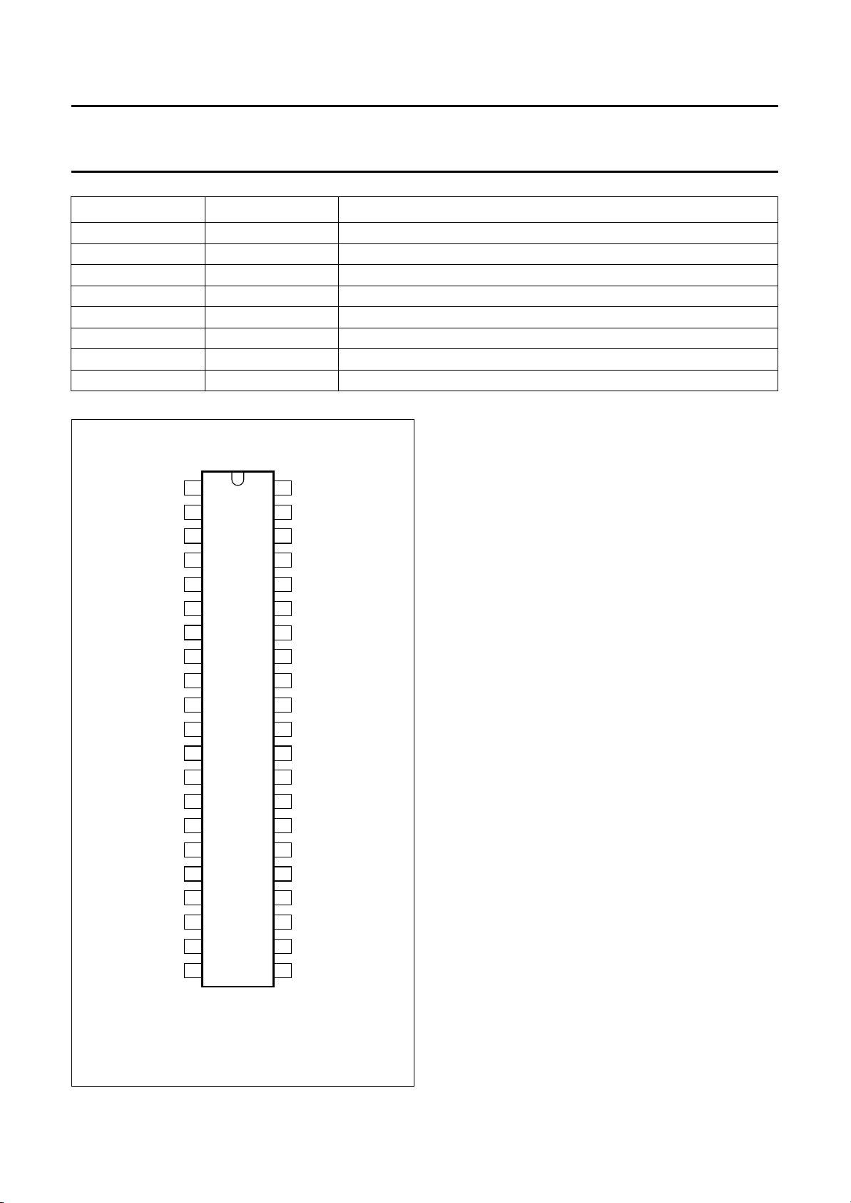
SYMBOL PIN DESCRIPTION
AVR 35 input automatic volume control, right channel
LIR 36 input line control, right channel
C
PS2
C
PS1
EOR 39 output effects, right channel
VIR 40 input volume, right channel
LDR 41 input loudness, right channel
OUTR 42 output, right channel
handbook, halfpage
OUTL
LDL
VIL
EOL
C
V
AVL
SOL
LOL
C
TW
C
C
VEO
VEI
C
NR
C
C
DEC
GND
SDA
AV
ref
LIL
TS
C
1
2
3
4
5
6
7
8
9
10
11
TDA9852
12
13
W
14
S
15
16
17
18
M
19
20
Fig.2 Pin configuration.
37 capacitor 2 pseudo function
38 capacitor 1 pseudo function
FUNCTIONAL DESCRIPTION
Stereo decoder
I
NPUT LEVEL ADJUSTMENT
The composite input signal is fed to the input level
adjustment stage. The control range is from
−3.5 to +4.0 dB in steps of 0.5 dB. The subaddress
control 3 of Tables 5 and 6 and the level adjust setting of
Table 21 allows an optimum signal adjustment during the
set alignment. The maximum input signal voltage is
2 V (RMS).
TEREO DECODER
S
The output signal of the level adjustment stage is coupled
to a low-pass filter which suppresses the baseband noise
above 125 kHz. The composite signal is then fed into a
pilot detector/pilot cancellation circuit and into the MPX
demodulator. The main L + R signal passes a 75 µs fixed
de-emphasis filter and is fed into the dematrix circuit.
The decoded sub-signal L − R is sent to the stereo/SAP
switch. To generate the pilot signal the stereo demodulator
uses a PLL circuit including a ceramic resonator.
The stereo channel separation is adjusted by an automatic
procedure to be performed during set production. For a
detailed description see Section “Adjustment procedure”.
The stereo identification can be read by the I2C-bus
(see Table 2). Two different pilot thresholds
(data STS = 1; STS = 0) can be selected via the I2C-bus
(see Table 19).
SAP
The composite signal is fed from the output of the input
level adjustment stage to the SAP demodulator circuit
MHA310
OUTR
42
LDR
41
VIR
40
EOR
39
C
38
PS1
C
37
PS2
LIR
36
AVR
35
SOR
34
LOR
33
C
32
SS
C
31
MO
CER
30
C
29
ADJ
C
28
PH
C
27
P2
C
26
P1
V
25
CAP
COMP
24
V
23
CC
SCL
2221
through a 5fH (fH= horizontal frequency) band-pass filter.
The demodulator level is automatically controlled. The
SAP demodulator includes internal noise and field strength
detectors that mute the SAP output in the event of
DEMODULATOR
TDA9852
1996 Feb 28 7
Page 8

Philips Semiconductors Preliminary specification
I2C-bus controlled BTSC stereo/SAP
decoder and audio processor
insufficient signal conditions. The SAP identification signal
can be read by the I2C-bus (see Table 2).
WITCH
S
The stereo/SAP switch feeds either the L − R signal or the
SAP demodulator output signal via the internal dbx noise
reduction circuit to the dematrix/switching circuit. Table 12
shows the different switch modes provided at the output
pins LOR and LOL.
dbx
DECODER
The circuit includes all blocks required for the noise
reduction system in accordance with the BTSC system
specification. The output signal is fed through a 73 µs fixed
de-emphasis circuit to the dematrix block.
NTEGRATED FILTERS
I
The filter functions necessary for stereo and SAP
demodulation and part of the dbx filter circuits are provided
on-chip using transconductor circuits. The required filter
accuracy is attained by an automatic filter alignment
circuit.
Audio processor
ELECTOR
S
The selector allows selecting either the internal line out
signals LOR or LOL (dematrix output) or the external line
in signals LIR and LIL and combines the left and right
signals in several modes (see Tables 5 and 6 for
subaddress and Table 11 for data). The input signal
capability of the line inputs (LIR/LIL) is 2 V (RMS). The
output of the selector is AC-coupled to the automatic
volume level control circuit via pins SOR/SOL and
AVR/AVL to avoid offset voltages.
UTOMATIC VOLUME LEVEL CONTROL
A
The automatic volume level stage controls its output
voltage to a constant level of typically 200 mV (RMS) from
an input voltage range of 0.1 to 1.1 V (RMS). The circuit
adjusts variations in modulation during broadcasting and
due to changes in the programme material. The function
can be switched off. To avoid audible ‘plops’ during the
permanent operation of the AVL circuit a soft blending
scheme has been applied between the different gain
stages. A capacitor (4.7 µF) at pin CAV determines the
attack and decay time constants. In addition the ratio of
attack and decay time can be changed via I2C-bus
(see Table 15). At power on, the discharged 4.7 µF
capacitor at CAV must be loaded by the internal decay
TDA9852
current. If AVL is chosen, this would result in an attenuated
AVL gain for about 10 seconds after poweron. This can be
speeded up by choosing via I
current (about 10 times higher) for about the first
2 seconds after power on (see Table 6, CCD bit in
control 1 and Table 18).
FFECTS
E
The audio processor section offers the following mode
selections: linear stereo, pseudo stereo, spatial stereo and
forced mono.The spatial mode provides an antiphase
crosstalk of 30% or 52% (switchable via I
see Table 10).
OLUME/LOUDNESS
V
The volume control range is from +16 dB to −71 dB in
steps of 1 dB and ends with a mute step (see Table 8).
Balance control is achieved by the independent volume
control of each channel. The volume control blocks
operate in combination with the loudness control. The filter
is linear when maximum gain for volume control is
selected. The filter characteristic changes automatically
over a range of 28 dB down to a setting of −12 dB.
At −12 dB volume control the maximum loudness boost is
obtained. The filter characteristic is determined by external
components. The proposed application provides a
maximum boost of 17 dB for bass and 4.5 dB for treble.
The loudness may be switched on or off via I2C-bus
control (see Table 9). The left and right volume control
stages include two independent zero crossing detectors.
A change in volume is automatically activated but not
executed. The execution is enabled at the next zero
crossing of the signal. If a new volume step is activated
before the previous one has been processed, the previous
value will be executed first, and then the new value will be
activated. If no zero crossing occurs the next volume
transmission will enforce the last activated volume setting.
The zero crossing is realized between adjoining steps and
between any steps, but not from any step to mute. In this
case the GMU bit is needed to use. In case only one
channel has to be muted, two steps are necessary.
The first step is a transmission of any step to −71 dB and
the second step is the−71 dB step to mute mode. The step
of −71 dB to mute mode has no zero crossing but this is
not relevant.
UTE
M
The mute function can be activated independently with last
step of volume control at the left or right output. By setting
the general mute bit GMU via the I2C-bus all outputs are
2
C-bus an increased charge
2
C-bus;
1996 Feb 28 8
Page 9

Philips Semiconductors Preliminary specification
I2C-bus controlled BTSC stereo/SAP
decoder and audio processor
muted. All channels include an independent zero cross
detector. The zero crossing mute feature can be selected
via bit TZCM:
TZCM = 0: forced mute with direct execution
TZCM = 1: execution in time with signal zero crossing.
In the zero cross mode a change in the GMU polarity is
activated but not executed. The execution is enabled at
the next zero crossing of the signal. To avoid a large delay
of mute switching, when very low frequencies are
processed, or the output signal amplitude is lower than the
DC offset voltage, the following I2C-bus transmissions are
needed:
a first transmission for mute execution
a second transmission about 100 ms later, which must
switch the zero crossing mode to forced mute
(TZCM = 0)
a third transmission to reactivate the zero crossing
mode (TZCM = 1). This transmission can take place
immediately, but must follow before the next mute
execution.
Adjustment procedure
OMPOSITE INPUT LEVEL ADJUSTMENT
C
Feed in from FM demodulator the composite signal with
100% modulation (25 kHz deviation) L + R; fi= 300 Hz.
Set input level control via I2C-bus monitoring line out
(500 mV ±20 mV). Store the setting in a non-volatile
memory.
A
UTOMATIC ADJUSTMENT PROCEDURE
• Capacitors of external inputs LIL and LIR must be
grounded at EIL and EIR
• Composite input signal L = 300 Hz, R = 3.1 kHz,
14% modulation for each channel; volume gain +16 dB
via I2C-bus
• Effects, AVL, loudness off.
TDA9852
• Line out setting bits: STEREO = 1, SAP = 0
(see Table 12)
• Selector setting SC0, SC1, SC2 = 0, 0, 0 (see Table 11)
• Start adjustment by transmission ADJ = 1 in register
ALI3; the decoder will align itself
• After 1 second minimum stop alignment by transmitting
ADJ = 0 in register ALI3 read the alignment data by an
2
C-bus read operation from ALR1 and ALR2
I
(see Chapter “I2C-bus protocol”) and store it in a
non-volatile memory; the alignment procedure
overwrites the previous data stored in ALI1 and ALI2
• Disconnect the capacitors of external inputs from
ground.
M
ANUAL ADJUSTMENT
Manual adjustment is necessary when no dual tone
generator is available (e.g. for service).
• Spectral and wideband data have to be set to 10000
(middle position for adjustment range)
• Composite input L = 300 Hz; 14% modulation
• Adjust channel separation by varying wideband data
• Composite input L = 3 kHz; 14% modulation
• Adjust channel separation by varying spectral data
• Iterative spectral/wideband operation for optimum
adjustment
• Store data in non-volatile memory.
IMING CURRENT FOR RELEASE RATE
T
Due to possible internal and external spreading, the timing
current can be adjusted via I2C-bus, see Table 20, as
recommended by dbx.
1996 Feb 28 9
Page 10

Philips Semiconductors Preliminary specification
I2C-bus controlled BTSC stereo/SAP
TDA9852
decoder and audio processor
Requirements for the composite input signal to ensure correct system performance
SYMBOL PARAMETER CONDITIONS MIN. TYP. MAX. UNIT
COMP
L+R(rms)
composite input level for 100%
modulation L + R
(25 kHz deviation);
RMS value; fi= 300 Hz
∆COMP composite input level
spreading under operating
conditions
Z
o
f
lf
f
hf
THD
L,R
output impedance note 1 − low-ohmic 5 kΩ
low frequency roll-off 25 kHz deviation L + R; −2dB −− 5Hz
high frequency roll-off 25 kHz deviation L + R; −2 dB 100 −−kHz
total harmonic distortion L + R fi= 1 kHz; 25 kHz deviation −− 0.5 %
S/N signal-to-noise ratio
L + R/noise
α
SB
side band suppression mono
into unmodulated SAP carrier;
SAP carrier/side band
α
SP
spectral spurious attenuation
L + R/spurious
measured at COMP 162 250 363 mV
= −20 to +70 °C; aging;
T
amb
−0.5 − +0.5 dB
power supply influence
= 1 kHz; 125 kHz deviation;
f
i
−− 1.5 %
note 2
CCIR 468-2 weighted quasi
peak; L + R; 25 kHz deviation;
= 1 kHz; 75 µs de-emphasis
f
i
critical picture modulation;
44 −−dB
note 3
with sync only 54 −−dB
mono signal: 25 kHz deviation,
46 −−dB
fi= 1 kHz; side band: SAP
carrier frequency ±1 kHz
50 Hz to 100 kHz;
mainly n × fH; no de-emphasis;
L + R; 25 kHz deviation,
f = 1 kHz as reference
n = 1, 5 35 −−dB
n = 4, 6 40 −−dB
n = 2, 3 26 −−dB
Notes
1. Low-ohmic preferred, otherwise the signal loss and spreading at COMP, caused by Z
impedance (see Chapter “Characteristics”, Section “Input level adjustment control”) must be taken into account.
2. In order to prevent clipping at over-modulation
(maximum deviation in the BTSC system for 100% modulation is 73 kHz).
3. For example colour bar or flat field white; 100% video modulation.
1996 Feb 28 10
and the composite input
O
Page 11
Philips Semiconductors Preliminary specification
I2C-bus controlled BTSC stereo/SAP
TDA9852
decoder and audio processor
LIMITING VALUES
In accordance with the Absolute Maximum Rating System (IEC 134).
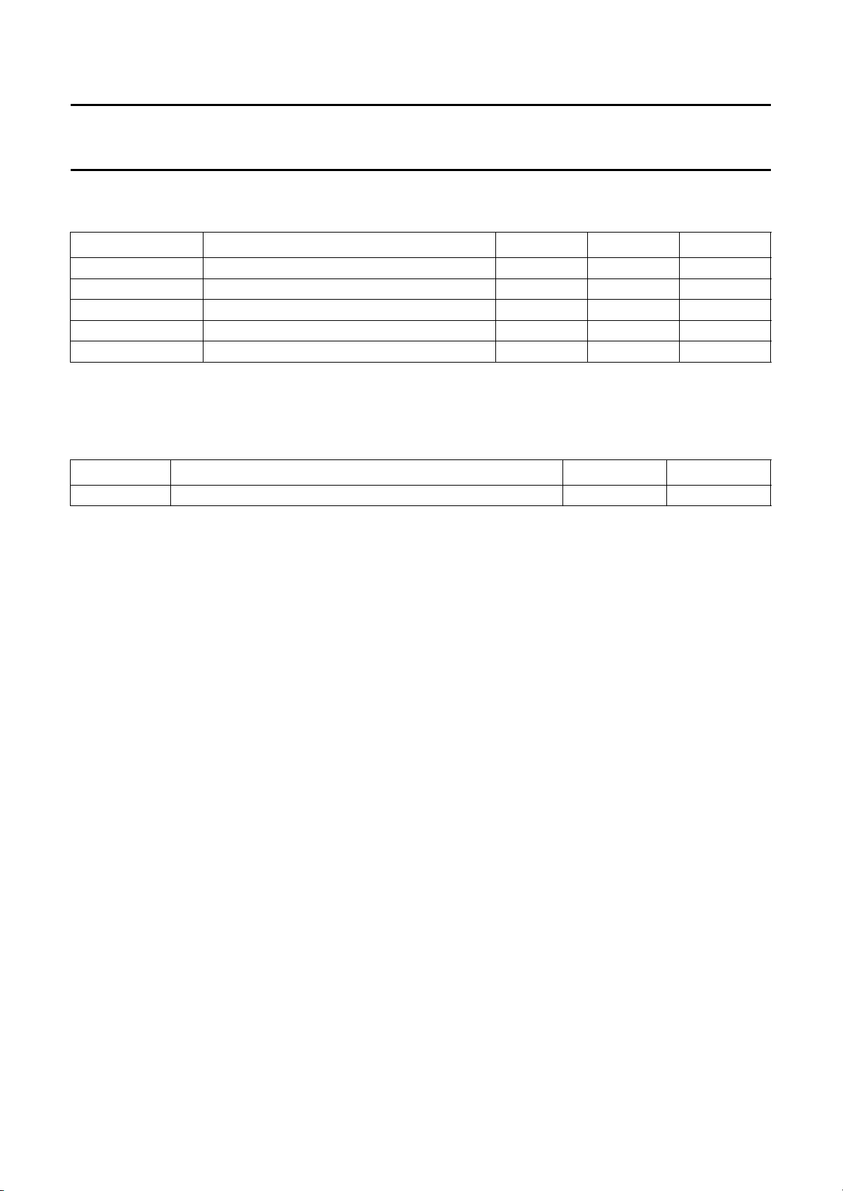
SYMBOL PARAMETER MIN. MAX. UNIT
V
CC
V
n
T
amb
T
stg
V
es
Note
1. Human body model: C = 100 pF; R = 1.5 kΩ; V = 2 kV; Charge device model: C = 200 pF; R = 0 Ω; V = 300 V.
THERMAL CHARACTERISTICS
SYMBOL PARAMETER VALUE UNIT
R
th j-a
supply voltage 0 9.5 V
voltage of all other pins to pin V
CC
0VCCV
operating ambient temperature −20 +70 °C
storage temperature −65 +150 °C
electrostatic handling; note 1
thermal resistance from junction to ambient in free air 43 K/W
1996 Feb 28 11
Page 12
Philips Semiconductors Preliminary specification
I2C-bus controlled BTSC stereo/SAP
TDA9852
decoder and audio processor
CHARACTERISTICS
All voltages are measured relative to GND; VCC= 8.5 V; Rs= 600 Ω; RL=10kΩ; CL= 2.5 nF; AC-coupled; fi= 1 kHz;
T
=25°C; gain control Gv= 0 dB; balance in mid position; loudness off; see Fig.1; unless otherwise specified.
amb
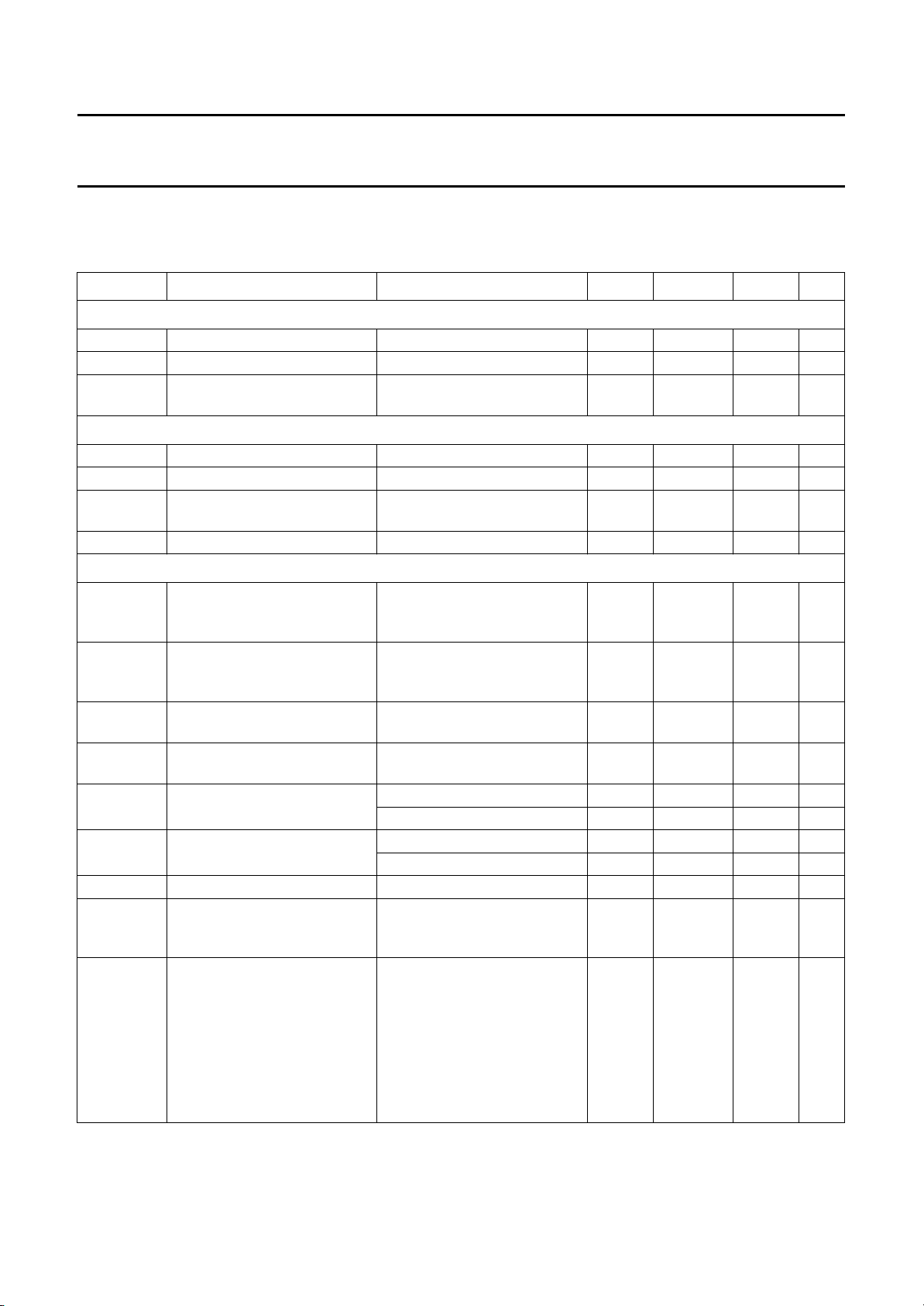
SYMBOL PARAMETER CONDITIONS MIN. TYP. MAX. UNIT
General
V
CC
I
CC
V
ref
Input level adjustment control
G
LA
G
step
V
i(rms)
Z
i
Stereo decoder
MPX
L+R(rms)
MPX
L−R
MPX
(max)
MPX
pilot(rms)
ST
on(rms)
ST
off(rms)
Hys hysteresis − 2.5 − dB
OUT
L+R
α
cs
supply voltage 8.0 8.5 9.0 V
supply current − 75 95 mA
internal reference voltage at
pin V
ref
− 4.25 − V
input level adjustment control −3.5 − +4.0 dB
step resolution − 0.5 − dB
maximum input voltage level
2 −−V
(RMS value)
input impedance 29.5 35 40.5 kΩ
input voltage level for 100%
modulation L + R;
25 kHz deviation (RMS value)
input voltage level for 100%
input level adjusted via I2C-bus
(L + R; fi= 300 Hz);
monitoring LINE OUT
− 250 − mV
− 707 − mV
modulation L − R;
50 kHz deviation (peak value)
maximum headroom for L + R,
f
< 15 kHz; THD < 15% 9 −−dB
mod
L, R
nominal stereo pilot voltage
− 50 − mV
level (RMS value)
pilot threshold voltage stereo
on (RMS value)
pilot threshold voltage stereo
off (RMS value)
output voltage level for 100%
modulation L + R at LINE OUT
data STS = 1 −− 35 mV
data STS = 0 −− 30 mV
data STS = 1 15 −−mV
data STS = 0 10 −−mV
input level adjusted via I2C-bus
480 500 520 mV
(L + R; fi= 300 Hz);
monitoring LINE OUT
stereo channel separation L/R
at LINE OUT
aligned with dual tone 14%
modulation for each channel;
see Section “Adjustment
procedure” in Chapter
“Functional description”
= 300 Hz; fR= 3 kHz 25 35 − dB
f
L
= 300 Hz; fR= 8 kHz 20 30 − dB
f
L
= 300 Hz; fR= 10 kHz 15 25 − dB
f
L
1996 Feb 28 12
Page 13
Philips Semiconductors Preliminary specification
I2C-bus controlled BTSC stereo/SAP
TDA9852
decoder and audio processor
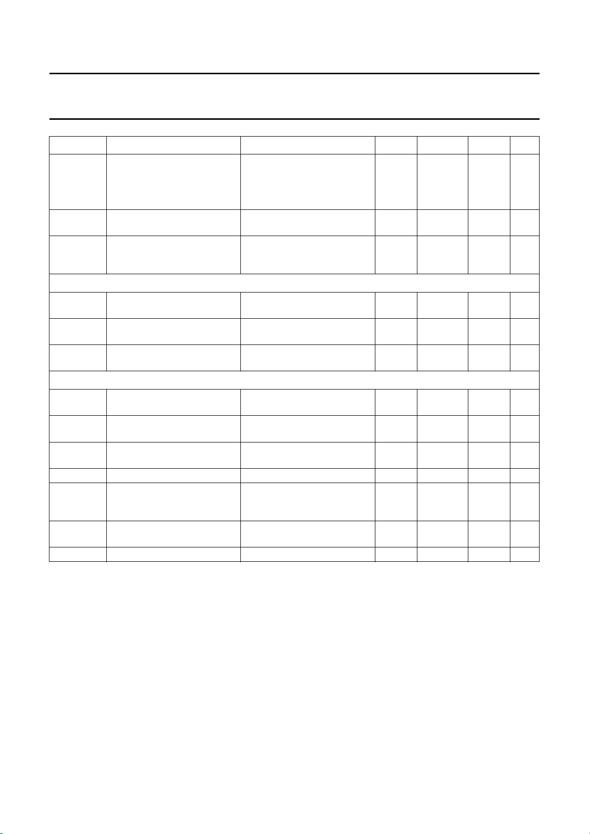
SYMBOL PARAMETER CONDITIONS MIN. TYP. MAX. UNIT
f
L, R
THD
L,R
S/N signal-to-noise ratio mono mode; CCIR 468-2
Stereo decoder, oscillator (VCXO); note 1
f
o
f
of
∆f
H
L, R frequency response 14% modulation;
f
= 300 Hz L or R
ref
=50Hzto10kHz −3 −−dB
f
i
= 12 kHz −−3 −dB
f
i
total harmonic distortion L, R
at LINE OUT
modulation L or R
1% to 100%; fi= 1 kHz
weighted; quasi peak;
500 mV output signal
nominal VCXO output
frequency (32fH)
spread of free-running
frequency
with nominal ceramic
resonator
with nominal ceramic
resonator
capture range frequency
(nominal pilot)
− 0.2 1.0 %
50 60 − dB
− 503.5 − kHz
500.0 − 507.0 kHz
±190 ±265 − Hz
SAP demodulator; note 2
SAP
i(rms)
nominal SAP carrier input
voltage level (RMS value)
SAP
on(rms)
threshold voltage SAP on
(RMS value)
SAP
off(rms)
threshold voltage SAP off
(RMS value)
SAP
SAP
hys
LEV
hysteresis − 2 − dB
SAP output voltage level at
LINE OUT
f
res
frequency response 14% modulation;
THD total harmonic distortion f
15 kHz frequency deviation of
− 150 − mV
intercarrier
−− 85 mV
35 −−mV
mode selector in position
SAP/SAP; f
= 300 Hz;
mod
− 500 − mV
100% modulation
−3 −−dB
50 Hz to 8 kHz; f
= 1 kHz − 0.5 2.0 %
i
= 300 Hz
ref
1996 Feb 28 13
Page 14
Philips Semiconductors Preliminary specification
I2C-bus controlled BTSC stereo/SAP
TDA9852
decoder and audio processor
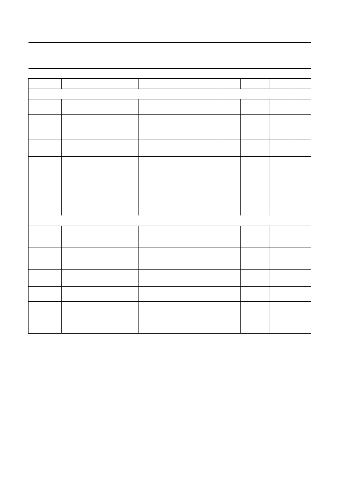
SYMBOL PARAMETER CONDITIONS MIN. TYP. MAX. UNIT
LINE OUT at pins LOL and LOR
V
o(rms)
HEAD
o
Z
o
V
O
R
L
C
L
α
ct
∆V
ST-SAP
nominal output voltage
(RMS value)
output headroom 9 −−dB
output impedance − 80 120 Ω
DC output voltage 0.45VCC0.5V
output load resistance 5 −−kΩ
output load capacitance −− 2.5 nF
crosstalk L, R into SAP 100% modulation; fi= 1 kHz;
crosstalk SAP into L, R 100% modulation; f
output voltage difference if
switched from L, R to SAP
100% modulation − 500 − mV
CC
0.55VCCV
50 75 − dB
L or R; mode selector switched
to SAP/SAP
= 1 kHz;
i
50 70 − dB
SAP; mode selector switched
to stereo
250 Hz to 6.3 kHz −− 3dB
dbx noise reduction circuit
t
adj
I
s
stereo adjustment time see Section “Adjustment
nominal timing current for
nominal release rate of
spectral RMS detector
∆I
s
I
s range
I
t
spread of timing current −15 − +15 %
timing current range 7 steps via I2C-bus −±30 − %
timing current for release rate
of wideband RMS detector
Rel
rate
nominal RMS detector
release rate
−− 1s
procedure” in Chapter
“Functional description”
Is can be measured at pin C
− 24 −µA
TS
via current meter connected to
1
⁄2VCC+1V
−
1
⁄3I
s
−µA
nominal timing current and
external capacitor values
wideband − 125 − dB/s
spectral − 381 − dB/s
1996 Feb 28 14
Page 15

Philips Semiconductors Preliminary specification
I2C-bus controlled BTSC stereo/SAP
TDA9852
decoder and audio processor
SYMBOL PARAMETER CONDITIONS MIN. TYP. MAX. UNIT
Circuit section from pins LIL and LIR to pins OUTL and OUTR; note 3
B roll-off frequencies C
THD total harmonic distortion V
RR ripple rejection V
α
ct
crosstalk between bus inputs
and signal outputs
V
no
α
cs
noise output voltage CCIR 468-2 weighted; quasi
channel separation Vi=1V; fi= 1 kHz 75 −−dB
Effect controls
α
α
spat1
spat2
anti-phase crosstalk by spatial
effect
ϕ phase shift by pseudo-stereo see Fig.3 −− −−
, C7, C10, C26, C27 and
6
C29= 2.2 µF; Zi = Z
i min
low frequency (−3 dB) −− 20 Hz
high frequency (−0.5 dB) 20 −−kHz
= 1000 mV; Gv= 0 dB;
i
− 0.2 0.5 %
AVL on
V
= 2000 mV; Gv= 0 dB;
i
− 0.2 0.5 %
AVL on
V
= 1000 mV; Gv= 0 dB;
i
− 0.02 − %
AVL off
= 2000 mV; Gv= 0 dB;
V
i
− 0.02 − %
AVL off
< 200 mV; fi= 100 Hz 47 50 − dB
r (rms)
notes 4 and 5 − 110 − dB
− 40 80 µV
peak; AVL off; loudness off;
Gv=0dB
measured in dBA; AVL off;
loudness off; G
=1V; fi= 12.5 kHz 75 −−dB
V
i
=0dB
v
− 8 −µV
− 52 − %
− 30 − %
1996 Feb 28 15
Page 16
Philips Semiconductors Preliminary specification
I2C-bus controlled BTSC stereo/SAP
TDA9852
decoder and audio processor
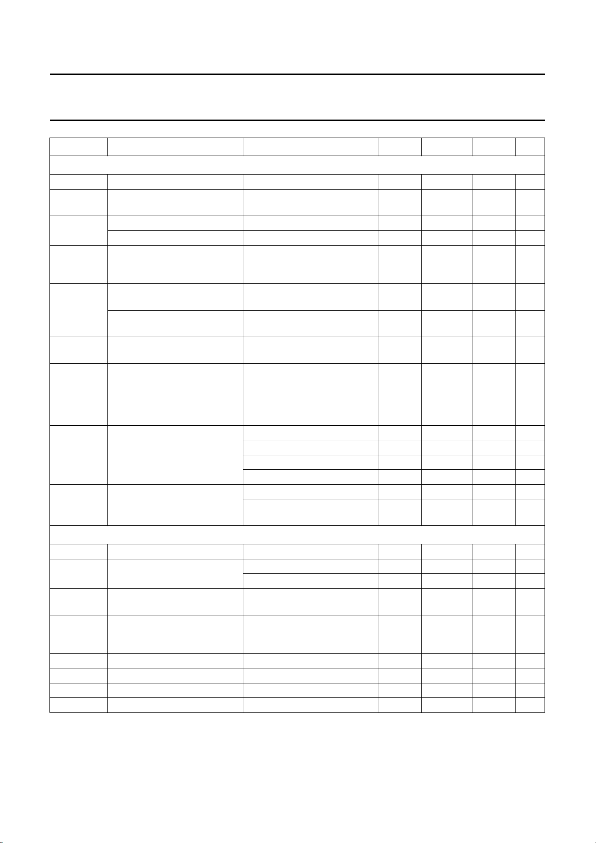
SYMBOL PARAMETER CONDITIONS MIN. TYP. MAX. UNIT
Automatic volume level control (AVL)
Z
i
V
i(rms)
G
v
G
step
V
iop(rms)
V
o(rms)
V
DC OFF
R
att
I
dec
input impedance 8.8 11.0 13.2 kΩ
maximum input voltage
THD < 0.2% 2 tbf − V
(RMS value)
gain, maximum boost 5 6 7 dB
maximum attenuation 14 15 16 dB
equivalent step width between
− 1.5 − dB
the input stages
(soft switching system)
input level at maximum boost
− 0.1 − V
(RMS value)
input level at maximum
− 1.125 − V
attenuation (RMS value)
output level in AVL operation
see Fig.4 160 200 250 mV
(RMS value)
DC offset between different
gain steps
voltage at pin C
6.50 to 6.33 V or
AV
−− 6mV
6.33 to 6.11 V or
6.11 to 5.33 V or
5.33 to 2.60 V; note 6
discharge resistors for attack
time constant
AT1 = 0; AT2 = 0; note 7 340 420 520 Ω
AT1 = 1; AT2 = 0; note 7 590 730 910 Ω
AT1 = 0; AT2 = 1; note 7 0.96 1.2 1.5 kΩ
AT1 = 1; AT2 = 1; note 7 1.7 2.1 2.6 kΩ
charge current for decay time normal mode; CCD = 0; note 8 1.6 2.0 2.4 µA
power-on speed-up; CCD = 1;
− tbf −µA
note 8
Selector from pins LOL, LOR, LIL and LIR to pins SOL and SOR
Z
α
V
i
s
i(rms)
input impedance 16 20 24 kΩ
input isolation of one selected
source to the other input
maximum input voltage
Vi=1V; fi= 1 kHz 86 96 − dB
V
=1V; fi= 12.5 kHz 80 96 − dB
i
THD < 0.5% 2 2.3 − V
(RMS value)
V
DC OFF
DC offset voltage at selector
output by selection of any
inputs
Z
o
R
L
C
L
G
v
output impedance − 80 120 Ω
output load resistance 5 −−kΩ
output load capacitance 0 − 2.5 nF
voltage gain, selector − 0 − dB
1996 Feb 28 16
−− 25 mV
Page 17
Philips Semiconductors Preliminary specification
I2C-bus controlled BTSC stereo/SAP
TDA9852
decoder and audio processor
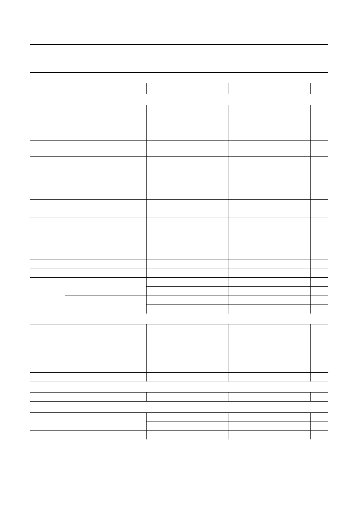
SYMBOL PARAMETER CONDITIONS MIN. TYP. MAX. UNIT
Audio control part; input pins VIL and VIR to pins OUTX and OUTS
Z
i
Z
o
R
L
C
L
V
i(rms)
V
no
G
c
G
step
∆G
a
∆G
L
α
m
V
DC OFF
Loudness control part
L
B
L
G
Muting at power supply drop for OUTR and OUTS
V
CC-DROP
Power-on reset; note 9
V
RESET(STA)
V
RESET(END)
volume input impedance 8.0 10.0 12.0 kΩ
output impedance − 80 120 Ω
output load resistance 5 −−kΩ
output load capacitance 0 − 2.5 nF
maximum input voltage
THD < 0.5% 2.0 2.15 − V
(RMS value)
noise output voltage CCIR 468-2 weighted;
quasi peak
=16dB − 110 220 µV
G
v
=0dB − 33 50 µV
G
v
mute position − 10 −µV
total continuous control range maximum boost − 16 − dB
maximum attenuation − 71 − dB
step resolution − 1 − dB
step error between adjoining
−− 0.5 dB
step
attenuator set error Gv= +16 to −50 dB −− 2dB
=−51 to −71 dB −− 3dB
G
v
gain tracking error Gv= +16 to −50 dB −− 2dB
mute attenuation 80 −−dB
DC step offset between any
adjacent step
DC step offset between any
step to mute
Gv= +16 to 0 dB − 0.2 10.0 mV
=0to−71 dB −− 5mV
G
v
= +16 to +1 dB − 215mV
G
v
=0to−71 dB − 110mV
G
v
maximum loudness boost loudness on; referred to
loudness off; boost is
determined by external
components; see Fig.5
=40Hz − 17 − dB
f
i
= 10 kHz − 4.5 − dB
f
i
loudness control range −12 − +16
supply drop for mute active − V
− 0.7 − V
CAP
start of reset voltage increasing supply voltage −− 2.5 V
decreasing supply voltage 4.2 5 5.8 V
end of reset voltage increasing supply voltage 5.2 6 6.8 V
1996 Feb 28 17
Page 18

Philips Semiconductors Preliminary specification
I2C-bus controlled BTSC stereo/SAP
TDA9852
decoder and audio processor
SYMBOL PARAMETER CONDITIONS MIN. TYP. MAX. UNIT
2
Digital part (I
V
IH
V
IL
I
IH
I
IL
V
OL
Notes to the characteristics
1. The oscillator is designed to operate together with MURAT A resonator CSB503F58. Change of the resonator supplier
is possible, but the resonator specification must be close to CSB503F58.
2. The internal SAP carrier level is determined by the composite input level and the level adjustment gain.
3. Frequency range 20 Hz to 20 kHz; select in to input line control; effects: linear stereo.
4. Crosstalk:
5. The transmission contains:
a) Total initialization with MAD and SAD for volume and 11 DATA words, see also definition of characteristics
b) Clock frequency = 50 kHz
c) Repetition burst rate = 400 Hz
d) Maximum bus signal amplitude = 5 V (p-p).
6. The listed pin voltage corresponds with typical gain steps of +6 dB, +3 dB, 0 dB, −6 dB and −15 dB.
7. Attack time constant = CAV× R
Decay time
8.
Example: C
9. When reset is active the GMU-bit (general mute) and the LMU-bit (LINE OUT mute) is set and the I
is in the reset position.
10. The AC characteristics are in accordance with the I2C-bus specification. The maximum clock frequency is 100 kHz.
Information about the I2C-bus can be found in the brochure
(order number 9398 393 40011).
C-bus pins); note 10
HIGH level input voltage 3 − V
CC
V
LOW level input voltage −0.3 − +1.5 V
HIGH level input current −10 − +10 µA
LOW level input current −10 − +10 µA
LOW level output voltage IIL=3mA −− +0.4 V
V
20 log
bus(p-p)
-------------------- V
o(rms)
.
att
G1–
----------
C
0.76 V× 10
AV
=
-------------------------------------------------------------------------------
= 4.7 µF; I
AV
dec
20
I
dec
=2µA; G1= −9 dB; G2=+6dB→ decay time results in 4.14 s.
G2–
---------20
10
–
2
C-bus receiver
“The I2C-bus and how to use it”
1996 Feb 28 18
Page 19
Philips Semiconductors Preliminary specification
I2C-bus controlled BTSC stereo/SAP
TDA9852
decoder and audio processor
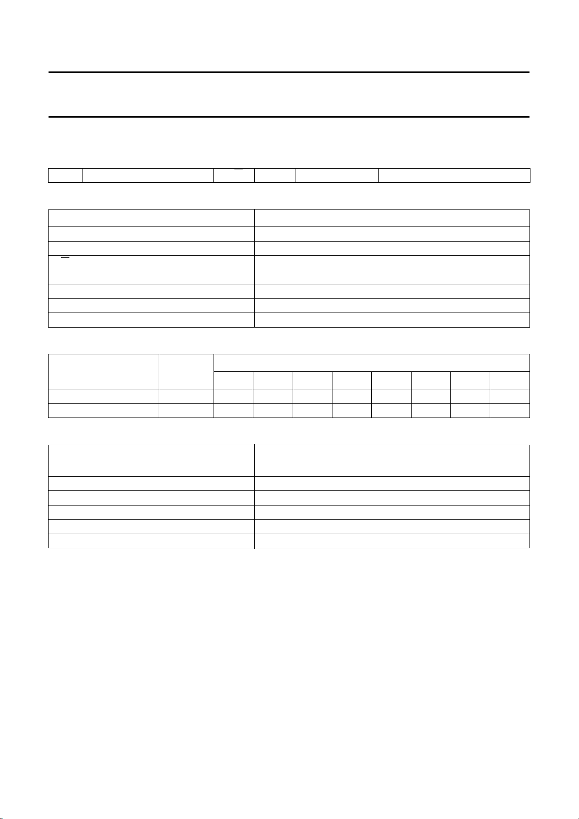
I2C-BUS PROTOCOL
2
C-bus format to read (slave transmits data)
I
S SLAVE ADDRESS R/
2
Table 1 Explanation of I
S START condition; generated by the master
Standard SLAVE ADDRESS (MAD) 101 101 1
W 1 (read); generated by the master
R/
A acknowledge; generated by the slave
DATA slave transmits an 8-bit data word
MA acknowledge; generated by the master
P STOP condition; generated by the master
Table 2 Definition of the transmitted bytes after read condition
FUNCTION BYTE
Alignment read 1 ALR1 Y SAPP STP A14 A13 A12 A11 A10
Alignment read 2 ALR2 Y SAPP STP A24 A23 A22 A21 A20
C-bus format to read (slave transmits data)
NAME DESCRIPTION
W A DATA MA DATA P
MSB LSB
D7 D6 D5 D4 D3 D2 D1 D0
Table 3 Function of the bits in Table 2
BITS FUNCTION
STP stereo pilot identification (stereo received = 1)
SAPP SAP pilot identification (SAP received = 1)
A1X to A2X stereo alignment read data
A1X for wideband expander
A2X for spectral expander
Y indefinite
The master generates an acknowledge when it has received the first data word ALR1, then the slave transmits the next
data word ALR2. Afterwards the master generates an acknowledge, then the slave begins transmitting the first data word
ALR1 etc. until the master generates no acknowledge and transmits a STOP condition.
1996 Feb 28 19
Page 20
Philips Semiconductors Preliminary specification
I2C-bus controlled BTSC stereo/SAP
TDA9852
decoder and audio processor
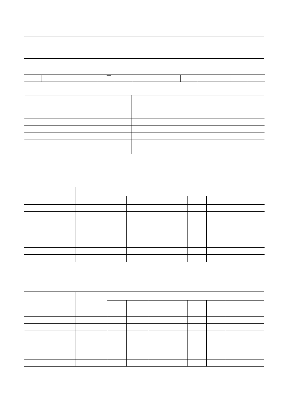
I2C-bus format to write (slave receives data)
S SLAVE ADDRESS R/
Table 4 Explanation of I
S START condition
Standard SLAVE ADDRESS (MAD) 101 101 1
W 0 (write)
R/
A acknowledge; generated by the slave
SUBADDRESS (SAD) see Table 5
DATA see Table 6
P STOP condition
If more than 1 byte of DATA is transmitted, then auto-increment is performed, starting from the transmitted subaddress
and auto-increment of subaddress in accordance with the order of Table 5 is performed.
Table 5 Subaddress second byte after MAD
2
C-bus format to write (slave receives data)
NAME DESCRIPTION
W A SUBADDRESS A DATA A P
FUNCTION REGISTER
Volume right VR 0 0 0 0 0 0 0 0
Volume left VL 0 0 0 0 0 0 0 1
Control 1 (note 1) CON1 0 0 0 0 0 1 0 1
Control 2 CON2 0 0 0 0 0 1 1 0
Control 3 CON3 0 0 0 0 0 1 1 1
Alignment 1 ALI1 0 0 0 0 1 0 0 0
Alignment 2 ALI2 0 0 0 0 1 0 0 1
Alignment 3 ALI3 0 0 0 0 1 0 1 0
Note
1. In auto-increment mode it is necessary to insert 3 dummy data words between volume left and control 1.
Table 6 Definition of third byte, third byte after MAD and SAD
FUNCTION REGISTER
Volume right VR 0 VR6 VR5 VR4 VR3 VR2 VR1 VR0
Volume left VL 0 VL6 VL5 VL4 VL3 VL2 VL1 VL0
Control 1 CON1 GMU AVLON LOFF CCD 0 SC2 SC1 SC0
Control 2 CON2 SAP STEREO TZCM 1 LMU EF2 EF1 EF0
Control 3 CON3 0 0 0 0 L3 L2 L1 L0
Alignment 1 ALI1 0 0 0 A14 A13 A12 A11 A10
Alignment 2 ALI2 STS 0 0 A24 A23 A22 A21 A20
Alignment 3 ALI3 ADJ AT1 AT2 0 1 TC2 TC1 TC0
MSB LSB
D7 D6 D5 D4 D3 D2 D1 D0
MSB LSB
D7 D6 D5 D4 D3 D2 D1 D0
1996 Feb 28 20
Page 21
Philips Semiconductors Preliminary specification
I2C-bus controlled BTSC stereo/SAP
TDA9852
decoder and audio processor
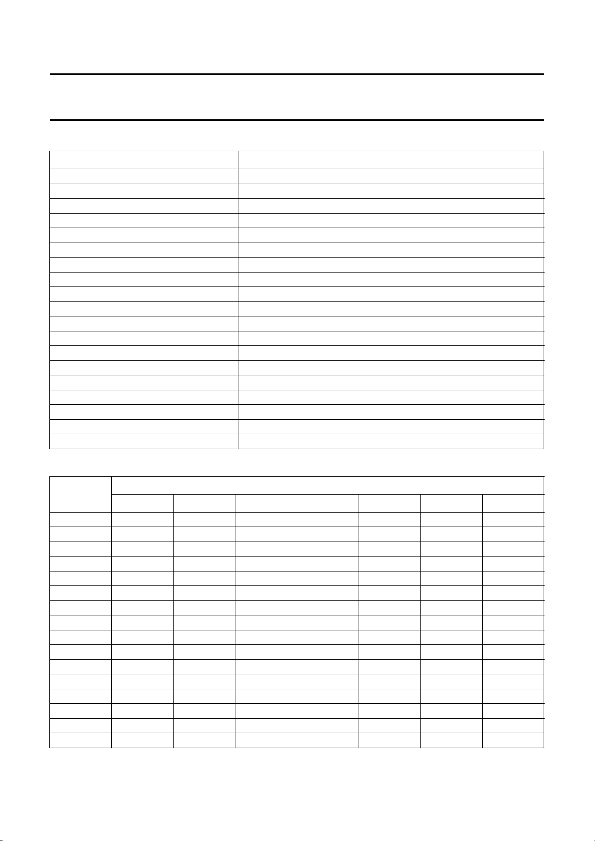
Table 7 Function of the bits in Table 6
BITS FUNCTION
VR0 to VR6 volume control right
VL0 to VL6 volume control left
GMU mute control for all outputs (generate mute)
AVLON AVL on/off
CCD increased AVL decay current on/off
LOFF switch loudness on/off
SC0 to SC2 selection between line in and line out
STEREO, SAP mode selection for line out
TZCM zero cross mode in mute operation (right and left output stage)
LMU mute control for line out
EF0 to EF2 selection between mono, stereo linear, spatial stereo and pseudo mode
L0 to L3 input level adjustment
ADJ stereo adjustment on/off
A1X to A2X stereo alignment data
A1X for wideband expander
A2X for spectral expander
AT1 and AT2 attack time at AVL
TC0 to TC2 timing current alignment data
STS stereo level switch
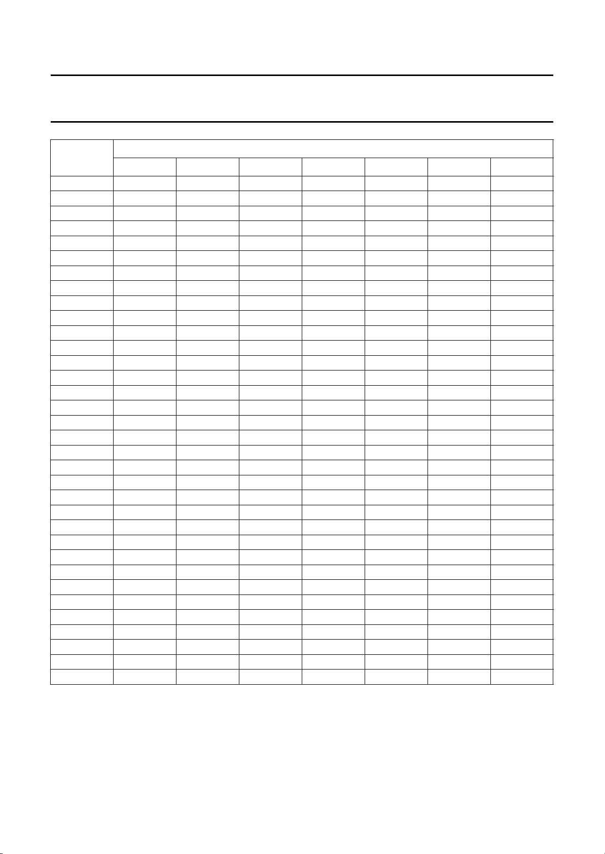
Table 8 Volume setting
FUNCTION
(dB)
G
v
161111111
151111110
141111101
131111100
121111011
111111010
101111001
91111000
81110111
71110110
61110101
51110100
41110011
31110010
21110001
11110000
V6 V5 V4 V3 V2 V1 V0
DATA
1996 Feb 28 21
Page 22
Philips Semiconductors Preliminary specification
I2C-bus controlled BTSC stereo/SAP
TDA9852
decoder and audio processor
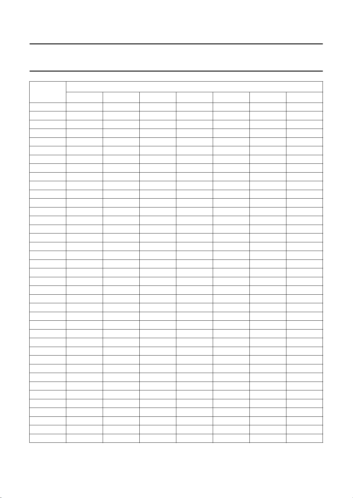
FUNCTION
(dB)
G
v
01101111
−11101110
−21101101
−31101100
−41101011
−51101010
−61101001
−71101000
−81100111
−91100110
−101100101
−111100100
−121100011
−131100010
−141100001
−151100000
−161011111
−171011110
−181011101
−191011100
−201011011
−211011010
−221011001
−231011000
−241010111
−251010110
−261010101
−271010100
−281010011
−291010010
−301010001
−311010000
−321001111
−331001110
−341001101
−351001100
−361001011
−371001010
−381001001
V6 V5 V4 V3 V2 V1 V0
DATA
1996 Feb 28 22
Page 23
Philips Semiconductors Preliminary specification
I2C-bus controlled BTSC stereo/SAP
TDA9852
decoder and audio processor
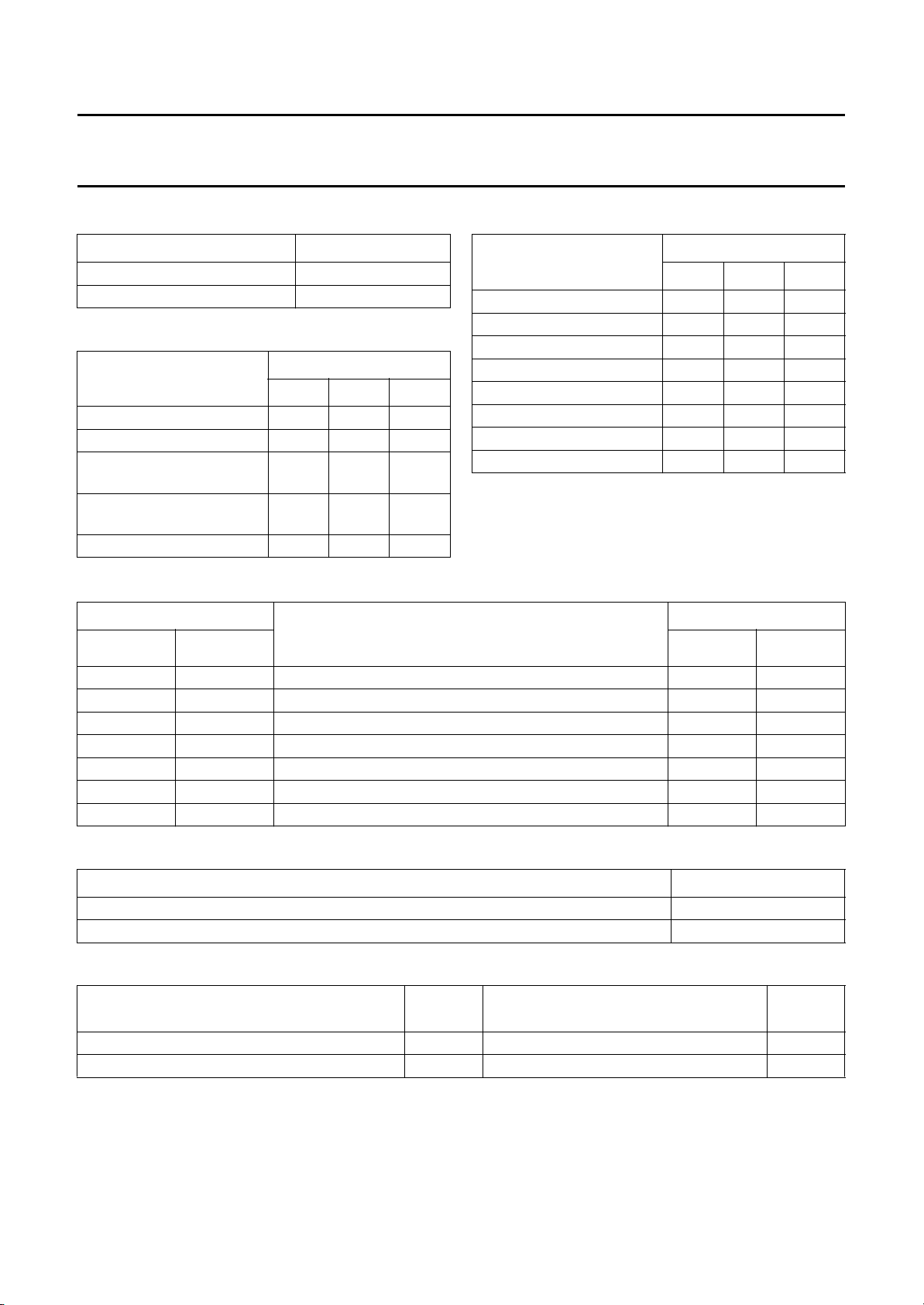
FUNCTION
(dB)
G
v
−391001000
−401000111
−411000110
−421000101
−431000100
−441000011
−451000010
−461000001
−471000000
−480111111
−490111110
−500111101
−510111100
−520111011
−530111010
−540111001
−550111000
−560110111
−570110110
−580110101
−590110100
−600110011
−610110010
−620110001
−630110000
−640101111
−650101110
−660101101
−670101100
−680101011
−690101010
−700101001
−710101000
Mute 0 1 00111
V6 V5 V4 V3 V2 V1 V0
DATA
1996 Feb 28 23
Page 24
Philips Semiconductors Preliminary specification
I2C-bus controlled BTSC stereo/SAP
decoder and audio processor
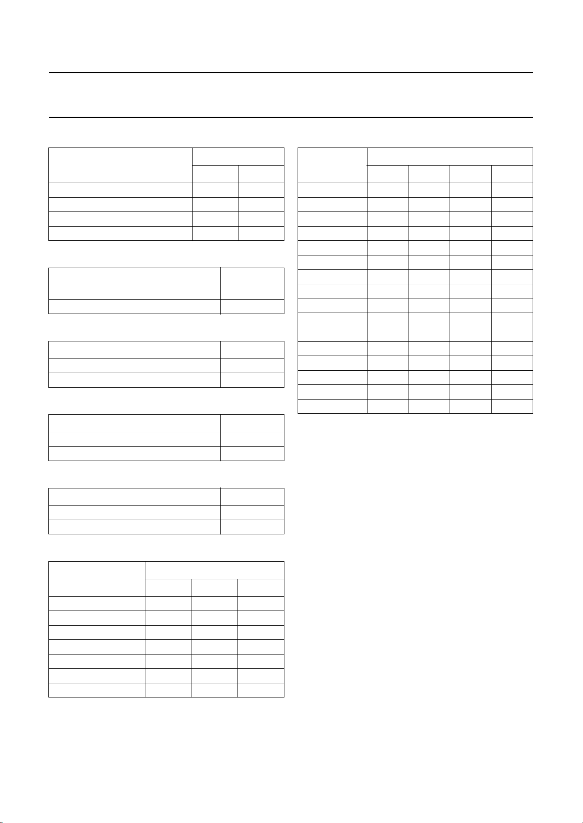
Table 9 Loudness setting
CHARACTERISTIC DATA LOFF
With loudness 0
Linear 1
Table 10 Effects setting
FUNCTION
EF2 EF1 EF0
Stereo linear on 000
Pseudo on 001
Spatial stereo;
30% anti-phase crosstalk
Spatial stereo;
50% anti-phase crosstalk
Forced mono 1 1 1
Table 12 Switch setting at line out
DATA
010
011
TDA9852
Table 11 Selector setting
FUNCTION
Inputs LOR and LOL 0 0 0
Inputs LOR and LOR 0 0 1
Inputs LOL and LOL 0 1 0
Inputs LOL and LOR 0 1 1
Inputs LIR and LIL 1 0 0
Inputs LIR and LIR 1 0 1
Inputs LIL and LIL 1 1 0
Inputs LIL and LIR 1 1 1
Note
1. Input connected to outputs SOR and SOL.
(1)
SC2 SC1 SC0
DATA
LINE OUT SIGNALS AT DATA
LOL LOR STEREO SAP
SAP SAP SAP received 1 1
Mute mute no SAP received 1 1
Left right STEREO received 1 0
Mono mono no STEREO received 1 0
Mono SAP SAP received 0 1
Mono mute no SAP received 0 1
Mono mono independent 0 0
Table 13 Zero cross detection setting
Direct mute control 0
Mute control delayed until the next zero crossing 1
Table 14 Mute setting
FUNCTION
Forced mute at OUTR, OUTL and OUTS 1 forced mute at LOR and LOL 1
Audio processor controlled outputs 0 stereo processor controlled outputs 0
INTERNAL SWITCH, READABLE BITS: STP, SAPP
FUNCTION DATA TZCM
TRANSMISSION STATUS
DATA
GMU
FUNCTION
SETTING BITS
DATA
LMU
1996 Feb 28 24
Page 25
Philips Semiconductors Preliminary specification
I2C-bus controlled BTSC stereo/SAP
decoder and audio processor
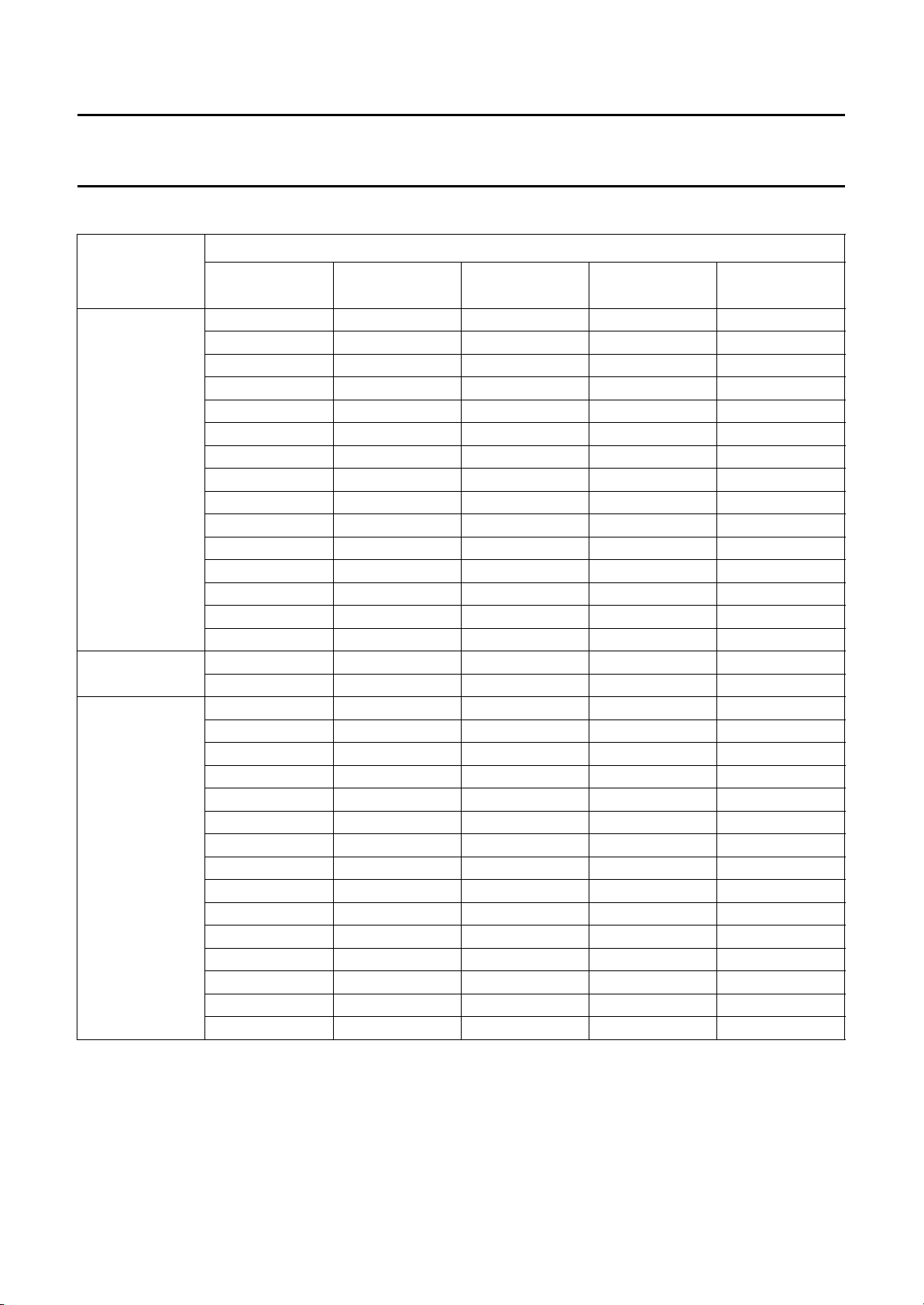
Table 15 AVL attack time
FUNCTION
= 420 Ω 00
R
att
= 730 Ω 10
R
att
= 1200 Ω 01
R
att
= 2100 Ω 11
R
att
Table 16 ADJ bit setting
FUNCTION DATA
Stereo decoder operation mode 0
Auto adjustment of channel separation 1
Table 17 AVLON bit setting
FUNCTION DATA
Automatic volume control off 0
Automatic volume control on 1
Table 18 CCD bit setting
DATA
AT1 AT2
TDA9852
Table 21 Level adjust setting
G
L
(dB)
L3 L2 L1 L0
+4.0 1111
+3.5 1110
+3.0 1101
+2.5 1100
+2.0 1011
+1.5 1010
+1.0 1001
+0.5 1000
0.0 0111
−0.5 0110
−1.0 0101
−1.5 0100
−2.0 0011
−2.5 0010
−3.0 0001
−3.5 0000
DATA
FUNCTION DATA
Load current for normal AVL decay time 0
Increased load current 1
Table 19 STS bit setting (pilot threshold stereo on)
FUNCTION DATA
≤ 35 mV 1
ST
on
ST
≤ 30 mV 0
on
Table 20 Timing current setting
FUNCTION
RANGE
I
S
TC2 TC1 TC0
DATA
+30% 1 0 0
+20% 1 0 1
+10% 1 1 0
Nominal 0 1 1
−10% 0 1 0
−20% 0 0 1
−30% 0 0 0
1996 Feb 28 25
Page 26
Philips Semiconductors Preliminary specification
I2C-bus controlled BTSC stereo/SAP
TDA9852
decoder and audio processor
Table 22 Alignment data for expander in read register ALR1 and ALR2 and in write register ALI1 and ALI2
DATA
FUNCTION
Gain increase 11111
Nominal gain 10000
Gain decrease 01110
D4
AX4
11110
11101
11100
11011
11010
11001
11000
10111
10110
10101
10100
10011
10010
10001
01111
01101
01100
01011
01010
01001
01000
00111
00110
00101
00100
00011
00010
00001
00000
D3
AX3
D2
AX2
D1
AX1
D0
AX0
1996 Feb 28 26
Page 27
Philips Semiconductors Preliminary specification
I2C-bus controlled BTSC stereo/SAP
decoder and audio processor
phase
(degree)
−100
−200
−300
−400
0
(1)
(2)
(3)
2
10
10
handbook, full pagewidth
TDA9852
MHA311
3
10
4
10
f (Hz)
5
10
(1) see Table 23.
(2) see Table 23.
(3) see Table 23.
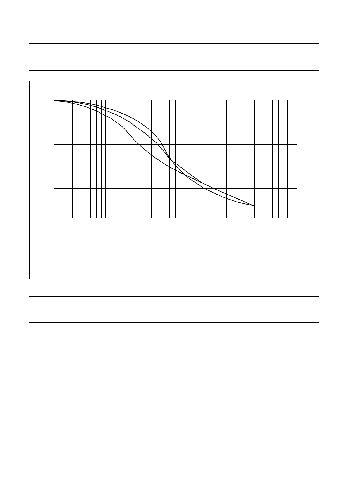
Fig.3 Pseudo (phase in degrees) as a function of frequency (left output).
Table 23 Explanation of curves in Fig.3
CURVE
CAPACITANCE AT PIN 38
(nF)
1 15 15 normal
2 5.6 47 intensified
3 5.6 68 more intensified
CAPACITANCE AT PIN 37
(nF)
EFFECT
1996 Feb 28 27
Page 28
Philips Semiconductors Preliminary specification
I2C-bus controlled BTSC stereo/SAP
decoder and audio processor
300
handbook, full pagewidth
V
o(rms)
(mV)
(1) V
(2) V
(3) V
250
200
160
100
10
CAV
o max(rms)
o min(rms)
−2
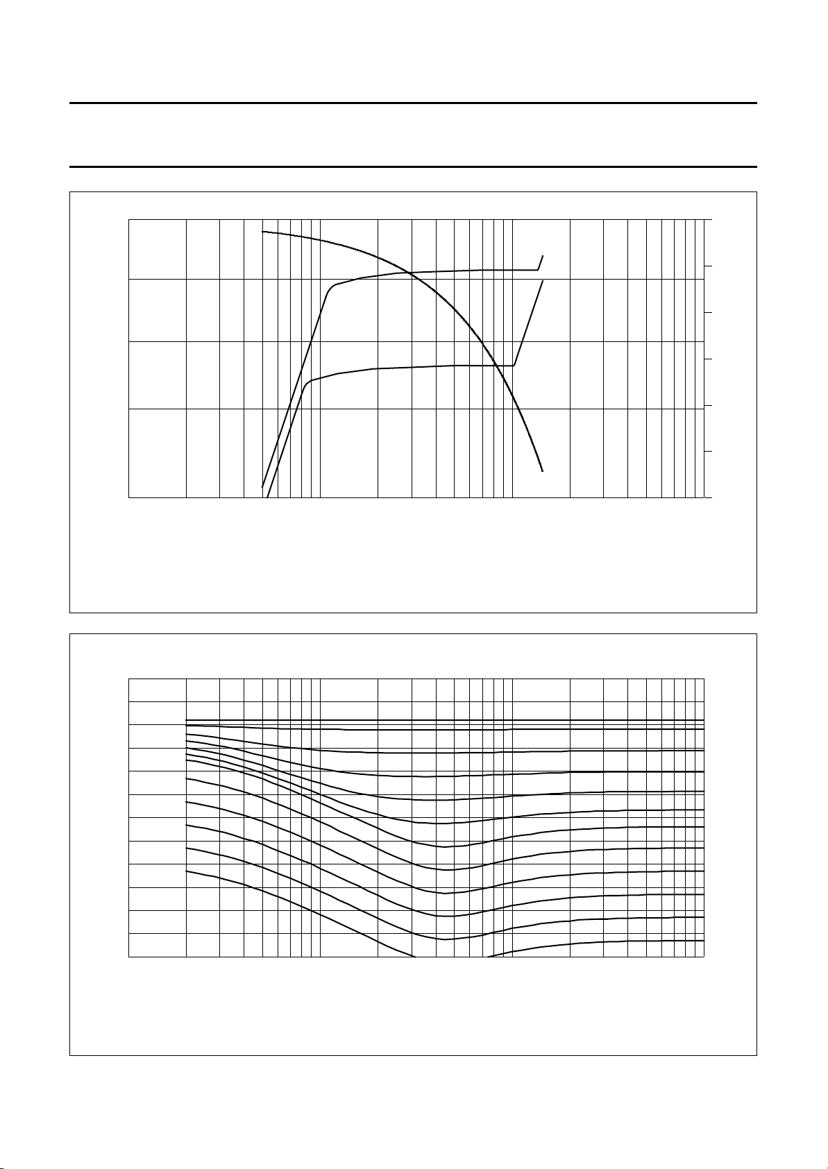
AVL measured at pin EOL/EOR.
Y1 axis output level in AVL operation with typically 200 mV.
Y2 axis V
DC voltage at pin CAV corresponds with typical gain steps in range of +6 to −15 dB.
CAV
10
Fig.4 Automatic level control diagram.
(1)
(2)
(3)
−1
1 1.4
TDA9852
MHA312
7
V
CAV
(V)
6
5
4
3
2
1
V
I(rms)
10
25
handbook, full pagewidth
(dB)
15
dB (VQX 0)
V
5
−5
−15
−25
−35
10 10
2
10
3
Fig.5 Volume control with loudness (including low roll-off frequency).
f (Hz)
MHA313
16
14
9
4
−1
−6
−11
parameter: volume gain setting (dB)
−16
−21
−26
−31
−36
4
10
1996 Feb 28 28
Page 29
Philips Semiconductors Preliminary specification
I2C-bus controlled BTSC stereo/SAP
decoder and audio processor
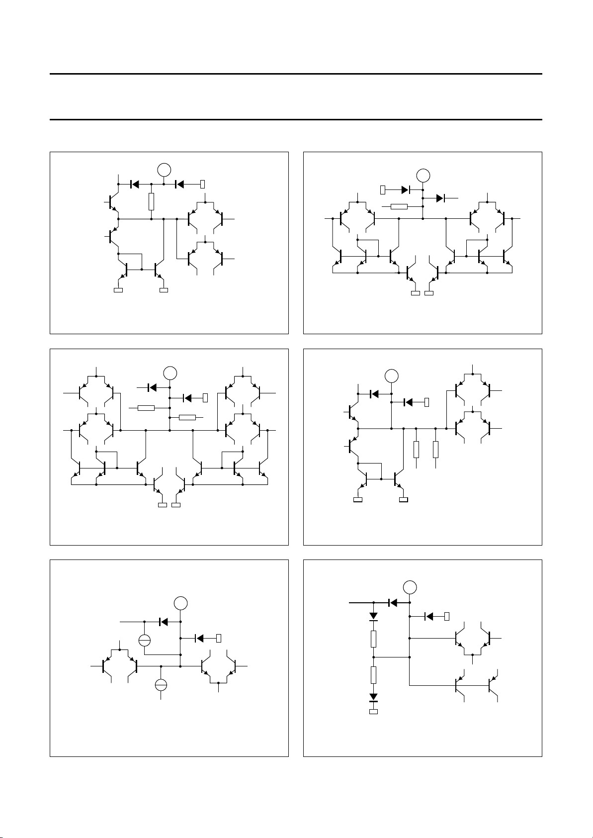
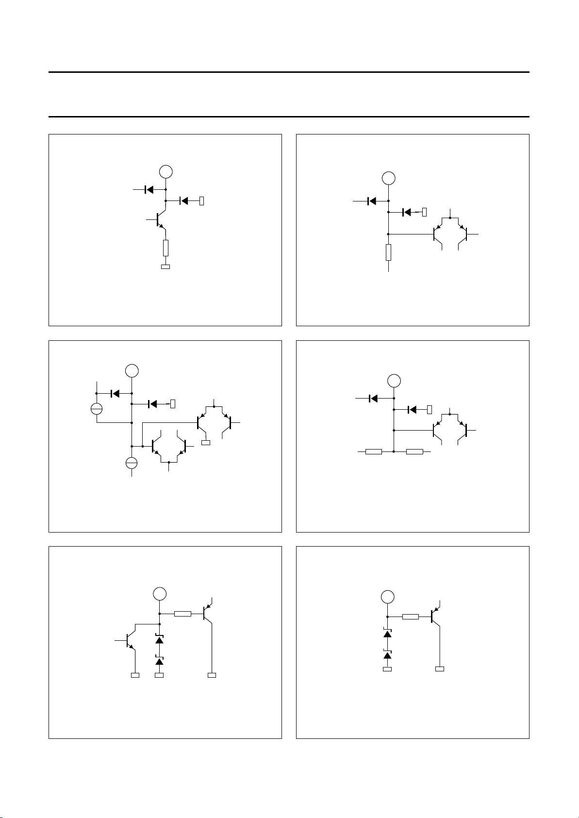
INTERNAL PIN CONFIGURATIONS
+
Fig.6 Pin 1: OUTL; pin 9: SOL; pin 34: SOR;
pin 42; OUTR.
+
10.58 kΩ
1 4.25 V
80 Ω
MHA314
3 4.25 V
4.8 kΩ
2 4.25 V
1.33 kΩ
+
Fig.7 Pin 2: LDL; pin 41: LDR.
+
4 4.25 V
TDA9852
MHA315
Fig.8 Pin 3: VIL; pin 40: VIR.
5
+
MHA318
MHA316
6.8
15
kΩ
kΩ
Fig.9 Pin 4: EOL; pin 39: EOR.
6
+
3.4
kΩ
3.4
kΩ
MHA317
MHA319
Fig.10 Pin 5: CAV.
1996 Feb 28 29
Fig.11 Pin 6: V
ref
.
Page 30
Philips Semiconductors Preliminary specification
I2C-bus controlled BTSC stereo/SAP
decoder and audio processor
7 4.25 V
+
20 kΩ 20 kΩ
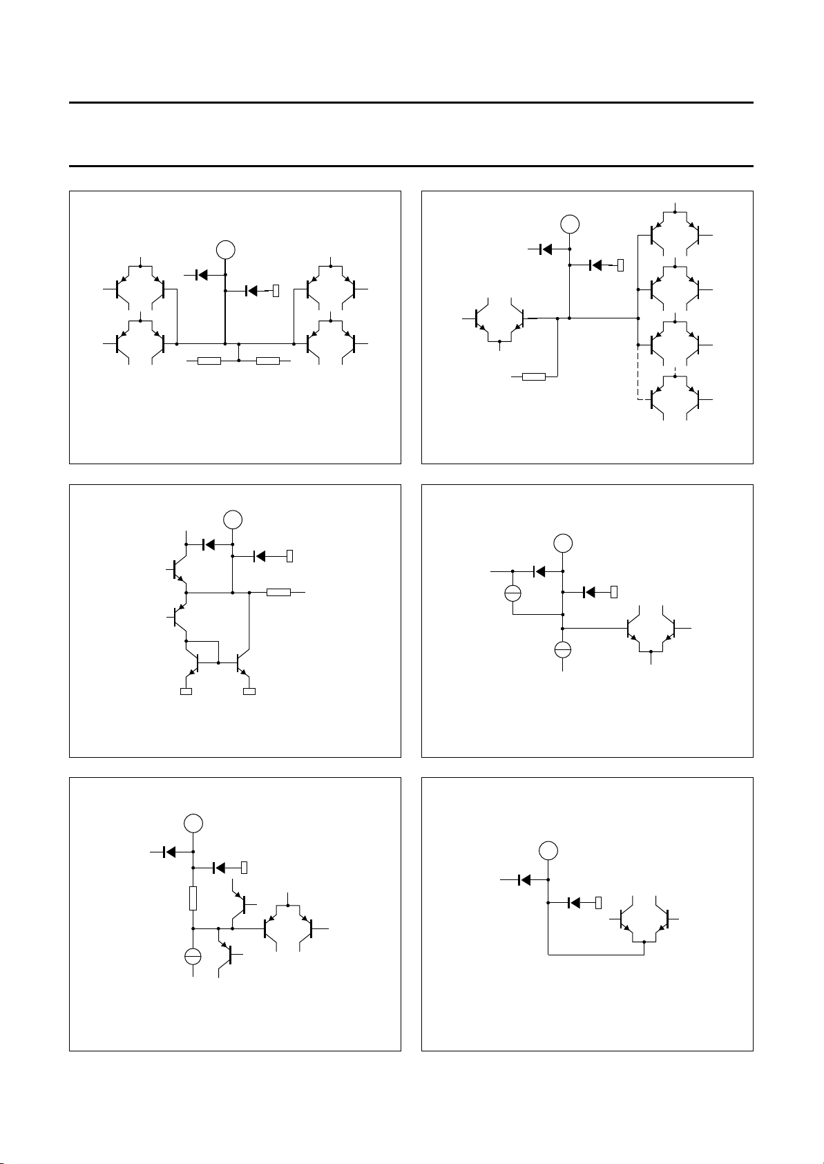
Fig.12 Pin 7: LIL; pin 36: LIR.
10
+
4.25 V
MHA320
TDA9852
8
4.25 V
+
1.75 kΩ
MHA321
Fig.13 Pin 8: AVL pin 35: AVR.
11
1
2
3
8
5 kΩ
MHA322
Fig.14 Pin 10: LOL; pin 33: LOR.
4.25 V
13
+
6
kΩ
MHA324
+
MHA323
Fig.15 Pin 11: CTW; pin 12: CTS.
15
+
MHA325
Fig.16 Pin 13: CW; pin 14: CS.
1996 Feb 28 30
Fig.17 Pin 15: VEO.
Page 31
Philips Semiconductors Preliminary specification
I2C-bus controlled BTSC stereo/SAP
decoder and audio processor
16
+
600 Ω
MHA326
Fig.18 Pin 16: VEI.
+
18
17
+
10
kΩ
Fig.19 Pin 17: CNR.
19 4.25 V
TDA9852
4.25 V
MHA327
MHA328
Fig.20 Pin 18: CM.
5 V
21
1.8 kΩ
MHA330
+
20 kΩ 20 kΩ
Fig.21 Pin 19: C
22 5 V
1.8 kΩ
MHA331
DEC
MHA329
.
Fig.22 Pin 21: SDA.
1996 Feb 28 31
Fig.23 Pin 22: SCL.
Page 32
Philips Semiconductors Preliminary specification
I2C-bus controlled BTSC stereo/SAP
decoder and audio processor
23
apply +8.5 V to this pin
+
MHA332
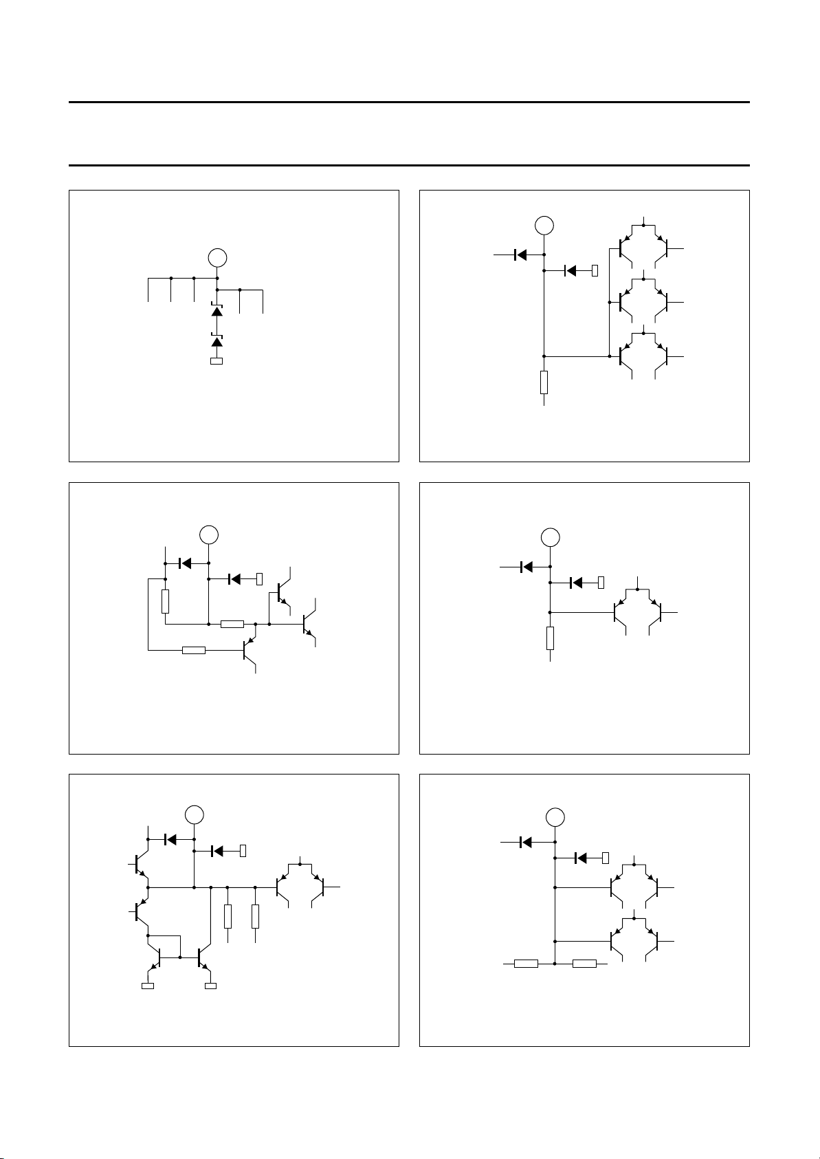
Fig.24 Pin 23: VCC.
24 4.25 V
+
30
kΩ
Fig.25 Pin 24: COMP.
TDA9852
MHA333
+
4.7
kΩ
5 kΩ
Fig.26 Pin 25: V
+
27 4.25 V
25
300 Ω
8.5
kΩ
12
kΩ
CAP
MHA334
.
MHA336
26 4.25 V
+
3.5
kΩ
Fig.27 Pin 26: CP1.
28 4.25 V
+
MHA335
Fig.28 Pin 27: CP2.
1996 Feb 28 32
10 kΩ 10 kΩ
Fig.29 Pin 28: CPH.
MHA337
Page 33
Philips Semiconductors Preliminary specification
I2C-bus controlled BTSC stereo/SAP
decoder and audio processor
+
29
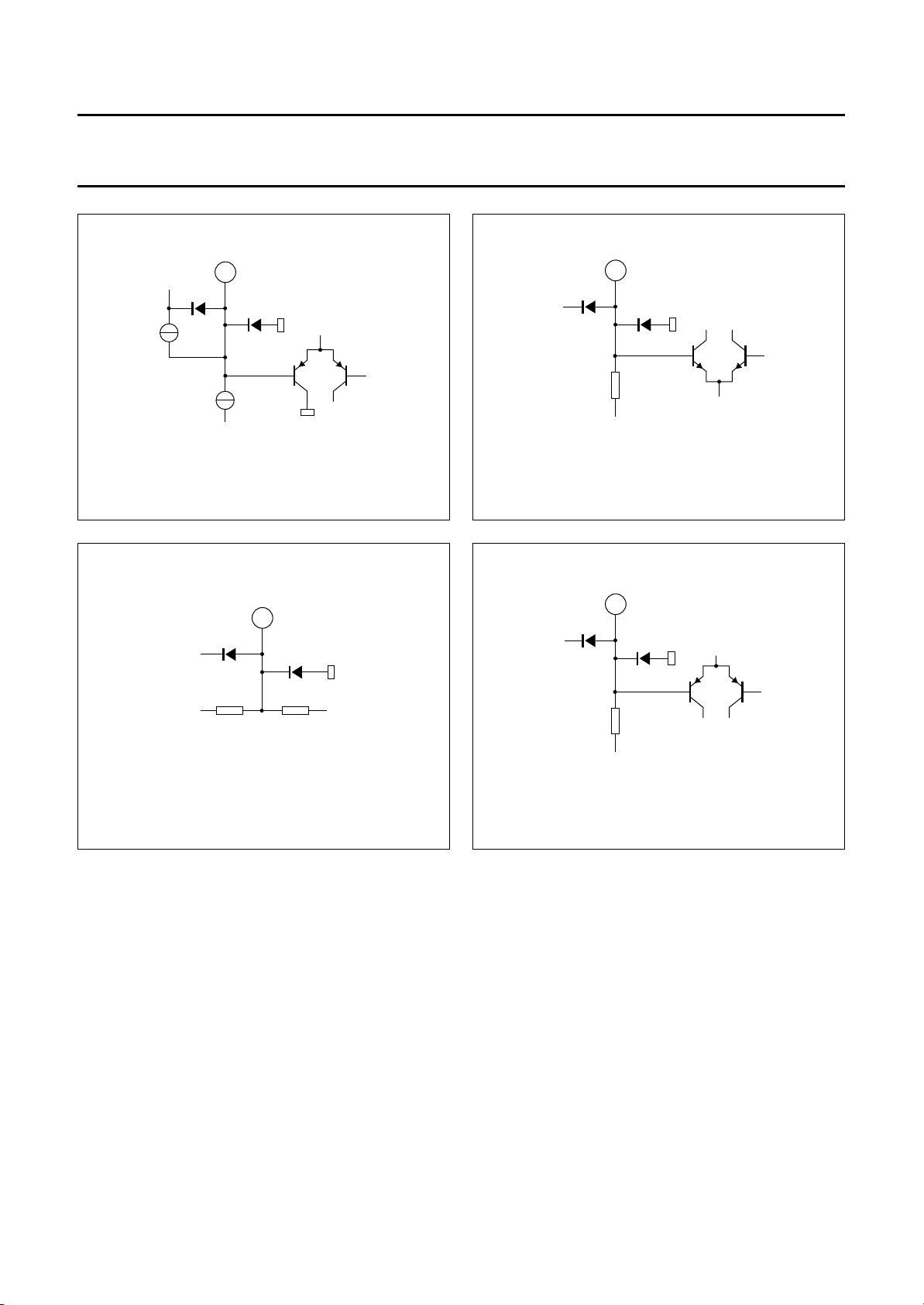
Fig.30 Pin 29: C
ADJ
MHA338
.
30
+
3
kΩ
Fig.31 Pin 30: CER.
TDA9852
MHA339
31 4.25 V
+
10 kΩ 10 kΩ
MHA340
Fig.32 Pin 31: CMO; pin 32: CSS.
38
+
15
kΩ
Fig.33 Pin 38: C
; pin 37: C
PS1
MHA341
PS2
.
1996 Feb 28 33
Page 34
Philips Semiconductors Preliminary specification
I2C-bus controlled BTSC stereo/SAP
decoder and audio processor
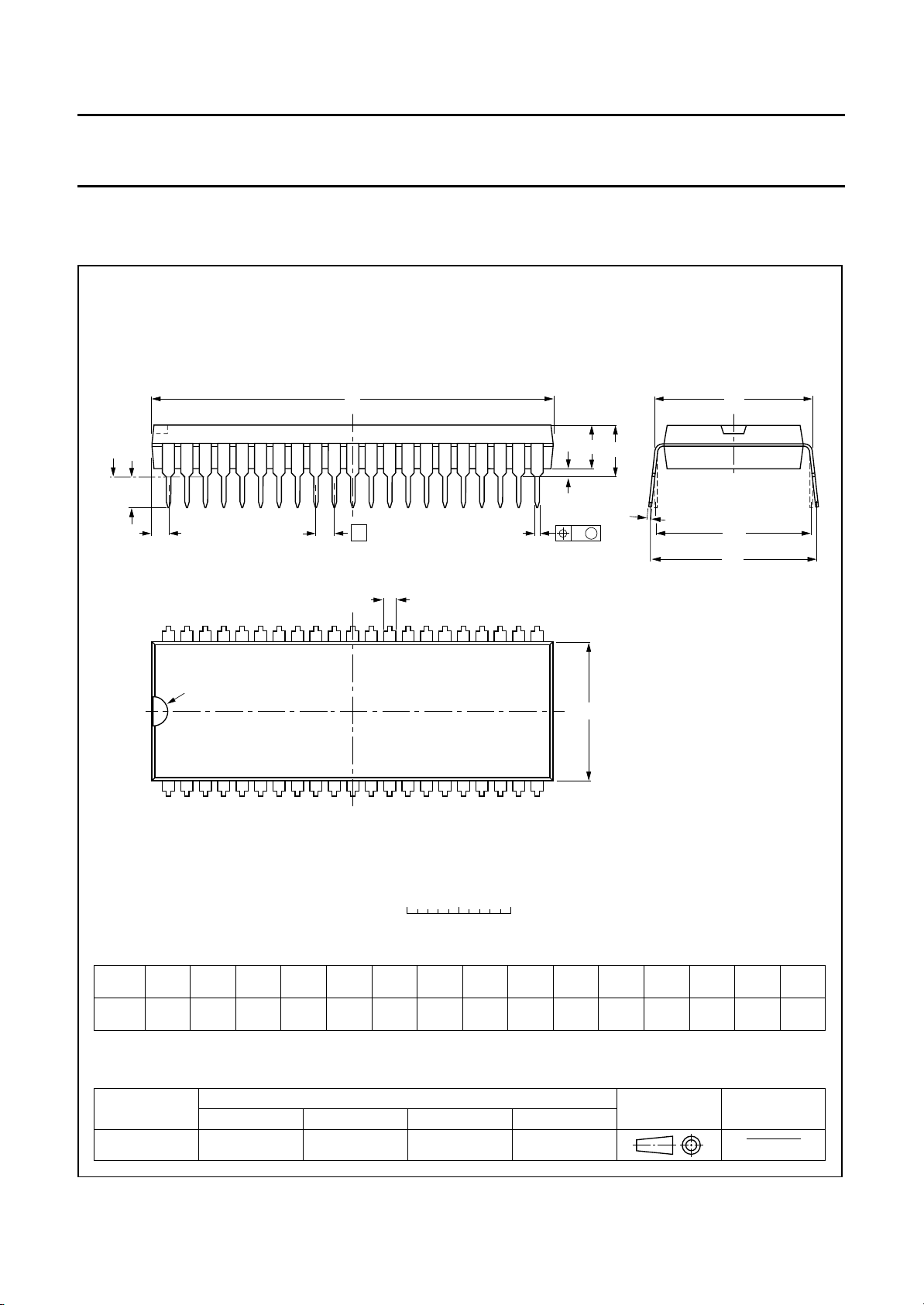
PACKAGE OUTLINE
SDIP42: plastic shrink dual in-line package; 42 leads (600 mil)
D
seating plane
L
Z
e
TDA9852
SOT270-1
M
E
A
2
A
A
1
w M
b
1
c
(e )
M
1
H
42
pin 1 index
1
DIMENSIONS (mm are the original dimensions)
A
A
A
UNIT b
max.
mm
5.08 0.51 4.0
12
min.
max.
b
1.3
0.8
0.53
0.40
b
22
E
21
0 5 10 mm
scale
cEe M
1
0.32
0.23
(1) (1)
D
38.9
38.4
14.0
13.7
1
L
M
E
3.2
15.80
2.9
15.24
17.15
15.90
e
w
H
0.181.778 15.24
Z
max.
1.73
(1)
Note
1. Plastic or metal protrusions of 0.25 mm maximum per side are not included.
OUTLINE
VERSION
SOT270-1
1996 Feb 28 34
REFERENCES
IEC JEDEC EIAJ
EUROPEAN
PROJECTION
ISSUE DATE
90-02-13
95-02-04
Page 35
Philips Semiconductors Preliminary specification
I2C-bus controlled BTSC stereo/SAP
decoder and audio processor
SOLDERING
Introduction
There is no soldering method that is ideal for all IC
packages. Wave soldering is often preferred when
through-hole and surface mounted components are mixed
on one printed-circuit board. However, wave soldering is
not always suitable for surface mounted ICs, or for
printed-circuits with high population densities. In these
situations reflow soldering is often used.
This text gives a very brief insight to a complex technology.
A more in-depth account of soldering ICs can be found in
our
“IC Package Databook”
Soldering by dipping or by wave
The maximum permissible temperature of the solder is
260 °C; solder at this temperature must not be in contact
DEFINITIONS
(order code 9398 652 90011).
TDA9852
with the joint for more than 5 seconds. The total contact
time of successive solder waves must not exceed
5 seconds.
The device may be mounted up to the seating plane, but
the temperature of the plastic body must not exceed the
specified maximum storage temperature (T
printed-circuit board has been pre-heated, forced cooling
may be necessary immediately after soldering to keep the
temperature within the permissible limit.
Repairing soldered joints
Apply a low voltage soldering iron (less than 24 V) to the
lead(s) of the package, below the seating plane or not
more than 2 mm above it. If the temperature of the
soldering iron bit is less than 300 °C it may remain in
contact for up to 10 seconds. If the bit temperature is
between 300 and 400 °C, contact may be up to 5 seconds.
stg max
). If the
Data sheet status
Objective specification This data sheet contains target or goal specifications for product development.
Preliminary specification This data sheet contains preliminary data; supplementary data may be published later.
Product specification This data sheet contains final product specifications.
Limiting values
Limiting values given are in accordance with the Absolute Maximum Rating System (IEC 134). Stress above one or
more of the limiting values may cause permanent damage to the device. These are stress ratings only and operation
of the device at these or at any other conditions above those given in the Characteristics sections of the specification
is not implied. Exposure to limiting values for extended periods may affect device reliability.
Application information
Where application information is given, it is advisory and does not form part of the specification.
LIFE SUPPORT APPLICATIONS
These products are not designed for use in life support appliances, devices, or systems where malfunction of these
products can reasonably be expected to result in personal injury. Philips customers using or selling these products for
use in such applications do so at their own risk and agree to fully indemnify Philips for any damages resulting from such
improper use or sale.
2
PURCHASE OF PHILIPS I
C COMPONENTS
1996 Feb 28 35
2
Purchase of Philips I
components in the I2C system provided the system conforms to the I2C specification defined by
Philips. This specification can be ordered using the code 9398 393 40011.
C components conveys a license under the Philips’ I2C patent to use the
 Loading...