

Page 1

INTEGRATED CIRCUITS
DATA SH EET
TDA9847
TV and VTR stereo/dual sound
processor with digital identification
Preliminary specification
Supersedes data of September 1993
File under Integrated Circuits, IC02
1995 May 23
Page 2

Philips Semiconductors Preliminary specification
TV and VTR stereo/dual sound processor
TDA9847
with digital identification
FEATURES
• Supply voltage 5 to 8 V
• Source selector
• Stereo matrix
• AF inputs for external stereo AF signals
(SCART or NICAM)
• AF outputs for main and SCART
• LED operation mode indication (stereo and dual)
• High identification reliability.
QUICK REFERENCE DATA
SYMBOL PARAMETER CONDITIONS MIN. TYP. MAX. UNIT
V
I
P
V
P
i(rms)
supply voltage (pin 22) 4.5 5 8.8 V
supply current (pin 22) without LED current 14 15 20 mA
nominal input signal voltage
54% modulation
Vi1to Vi4 (RMS value)
V
o(rms)
nominal output signal voltage
54% modulation − 500 − mV
(RMS value)
V
o(rms)
clipping level of the output signal
THD ≤ 1.5%; B/G or L
voltages (RMS value)
I
V
Lon
i pil
input current LED on −−12 mA
input voltage sensitivity of pilot
unmodulated 5 − 100 mV
frequency
S/N(W) weighted signal-to-noise ratio
“CCIR468-3”
THD total harmonic distortion − 0.2 0.3 %
T
f
ident
amb
operating ambient temperature 0 − +70 °C
identification window width stereo 2.2 − 2.2 Hz
dual 2.3 − 2.3 Hz
t
ident on
V
i tuner
∆f
pil
total identification time on 0.35 − 2.0 s
identification voltage sensitivity − 28 − dBµV
pull-in frequency range of pilot PLL f
osc
GENERAL DESCRIPTION
The TDA9847 is a stereo/dual sound processor for TV and
VTR sets. Its identification ensures safe operation by using
internal digital PLL technique with extremely small
bandwidth, synchronous detection and digital integration
(switching time maximum 2.0 s; identification concerning
the main functions).
B/G − 250 − mV
L − 500 − mV
= 5 V 1.4 1.60 − V
V
P
= 8 V 2.4 2.65 − V
V
P
66 75 − dB
= 10.008 MHz
lower side −296 −−296 Hz
upper side 302 − 302 Hz
ORDERING INFORMATION
TYPE
NUMBER
NAME DESCRIPTION VERSION
PACKAGE
TDA9847 SDIP24 plastic shrink dual in-line package; 24 leads (400 mil) SOT234-1
TDA9847T SO24 plastic small outline package; 24 leads; body width 7.5 mm SOT137-1
1995 May 23 2
Page 3
Philips Semiconductors Preliminary specification
TV and VTR stereo/dual sound processor
with digital identification
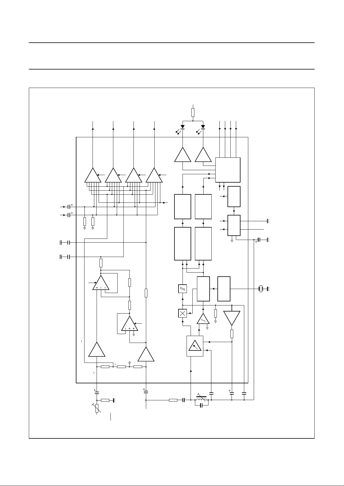
BLOCK DIAGRAMS
i3
V
i4
SCART
V
250 mV
250 mV RMS
RMS
±5%
10 nF
D2
C
D1
C
±5%
10 nF
2.2 µF 2.2 µF
17 21 12 11
o1
V
14
500 mV RMS
6 dB
50 kΩ
refVref
V
50 kΩ
5 kΩ
main
V
RMS
AM
250 mV
o2
13
500 mV RMS
6 dB
L/A/mono
o3
V
16
500 mV RMS
6 dB
RMS250 mV
L
SCART
o4
V
15
500 mV RMS
R/B
250 mV RMS
6 dB
V
1 kΩ
stereo transmission
19
dual bit
(274 Hz)
mute
DIGITAL
INTEGRATOR
AND
DIGITAL PLL
DEMODULATOR
P
18
bit
stereo
DIGITAL
AND
DIGITAL PLL
C1C2C3
dual transmission
1
2
(117 Hz)
INTEGRATOR
DEMODULATOR
C4
3
24
LOGIC
CONTROL
RESET
POWER-ON
SUPPLY
ref
V
202223 8
MED803
P
1/2 V
P
V
ref
C
100 µF/
16 V
TDA9847
A/mono
5 kΩ
6 dB (AM)
2.2 µF
2.2 kΩ
0 dB
3 dB
3 dB
9
V
10 kΩ 10 kΩ
ref
V
ref
0 dB
V
3 dB
15 kΩ
35 kΩ
50 kΩ
10
2.2 kΩ
, A
2
i1
L + R
250 mV RMS
(AM: 500 mV RMS)
V
TDA9847
2.2 µF
R, B
i2
250 mV RMS
1995 May 23 3
PLL
DIGITAL
7
= 70
o
2.5 mH
Q
47 pF
30 kΩ
FP
FP
R
C
3.3 nF
tan δ ≤ 0.002
V
ref
6
C
25 kΩ
DCL
ref
V
100 nF
OSCILLATOR
25 kΩ
4
10 µF
AGC
C
10 MHz
Fig.1 Block diagram of the bipolar TV/VTR-stereo decoder.
5
10 nF
LP
C
Input and output levels are nominal values related to the SCART norm (AM: m =0.54, FM: ∆f=±27 kHz).
Page 4
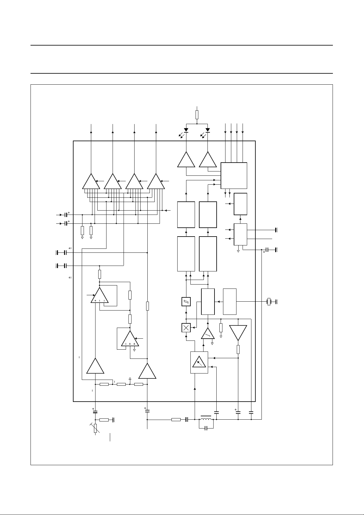
Philips Semiconductors Preliminary specification
TV and VTR stereo/dual sound processor
with digital identification
i3
V
i4
SCART
V
250 mV
250 mV RMS
RMS
5%
10 nF
D2
C
D1
C
5%
10 nF
2.2 µF 2.2 µF
17 21 12 11
o1
V
14
500 mV RMS
6 dB
50 kΩ
refVref
V
50 kΩ
5 kΩ
main
V
RMS
AM
250 mV
o2
13
500 mV RMS
6 dB
L/A/mono
o3
V
16
500 mV RMS
6 dB
RMS250 mV
L
SCART
o4
V
15
500 mV RMS
R/B
250 mV RMS
stereo transmission
19
6 dB
dual bit
mute
DIGITAL
INTEGRATOR
AND
DIGITAL PLL
P
V
1 kΩ
18
bit
stereo
(274 Hz)
DEMODULATOR
(117 Hz)
DIGITAL
INTEGRATOR
AND
DIGITAL PLL
DEMODULATOR
C1C2C3
dual transmission
1
2
24
LOGIC
CONTROL
POWER-ON
V
C4
3
RESET
SUPPLY
ref
202223 8
MED804
P
1/2 V
TDA9847
P
V
ref
C
100 µF/
16 V
A/mono
5 kΩ
6 dB (AM)
2.2 µF
2.2 kΩ
0 dB
3 dB
3 dB
9
V
10 kΩ 10 kΩ
ref
V
ref
0 dB
V
3 dB
15 kΩ
35 kΩ
50 kΩ
10
2.2 kΩ
, A
2
i1
L + R
250 mV RMS
(AM: 500 mV RMS)
V
2.2 µF
R, B
i2
TDA9847
250 mV RMS
27 kΩ
FP
R
1995 May 23 4
180 pF
FP
C
7
±5%
4.7 mH
1.8 nF
PLL
DIGITAL
ref
V
6
= 25
o
Q
±2%
tan δ ≤ 0.01
C
25 kΩ
V
DCL
OSCILLATOR
ref
100 nF
10 MHz
25 kΩ
Fig.2 Block diagram of the bipolar TV/VTR-stereo decoder with fixed coil (alignment-free).
5
4
10 nF
10 µF
LP
C
AGC
C
Input and output levels are nominal values related to the SCART norm (AM: m = 0.54, FM: ∆f=±27 kHz).
The components of the external LC band-pass filter have the following order-No.: Philips Germany only No: 4312 020 17525 or Fastron Sdn. Bha., Malaysia type SMCC 472 J
for L = 4.7 MHz (±5%) Philips Components No: 2222 429 71802, C = 1.8 nF (±2%).
Page 5
Philips Semiconductors Preliminary specification
TV and VTR stereo/dual sound processor
with digital identification
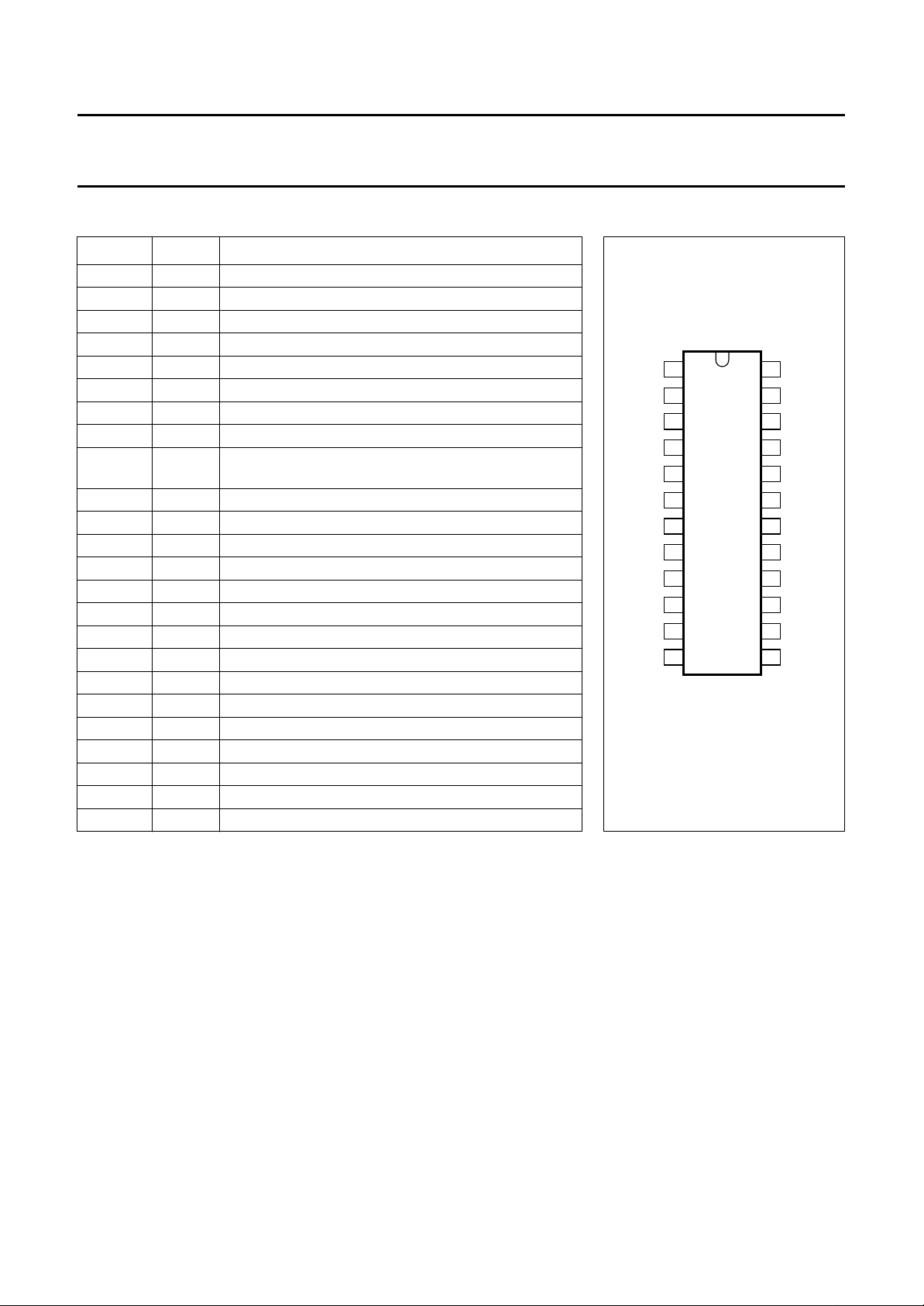
PINNING
SYMBOL PIN DESCRIPTION
C1 1 control input Port C1
C2 2 control input Port C2
C4 3 control input Port C4
C
AGC
C
LP
C
DCL
V
i pil
C
ref
V
i1
V
i2
V
i3
V
i4
V
o2
V
o1
V
o4
V
o3
C
D1
LEDDU 18 LED (dual)
LEDST 19 LED (stereo)
GND 20 ground (0 V)
C
D2
V
P
XTAL 23 10 MHz crystal input
C3 24 control input Port C3
4 AGC capacitor of pilot frequency amplifier
5 identification low-pass capacitor
6 DC loop capacitor
7 pilot frequency input voltage
8 capacitor of reference voltage (1⁄2VP)
9 AF input signal voltage 1 [from sound carrier 1 or
AM sound (standard L)]
10 AF input signal voltage 2 (from sound carrier 2)
11 AF input signal voltage 3 (SCART)
12 AF input signal voltage 4 (SCART)
13 AF output signal voltage 2 (main)
14 AF output signal voltage 1 (main)
15 AF output signal voltage 4 (SCART)
16 AF output signal voltage 3 (SCART)
17 50 µs de-emphasis capacitor of AF Channel 1
21 50 µs de-emphasis capacitor of AF Channel 2
22 supply voltage (5 to 8 V)
TDA9847
1
C1
2
C2
3
C4
4
C
AGC
5
C
LP
6
C
DCL
V
i pil
C
ref
V
V
V
V
Fig.3 Pin configuration.
TDA9847
7
8
9
i1
10
i2
11
i3
12
i4
MED805
24
23
22
21
20
19
18
17
16
15
14
13
C3
XTAL
V
P
C
D2
GND
LEDST
LEDDU
C
D1
V
o3
V
o4
V
o1
V
o2
1995 May 23 5
Page 6

Philips Semiconductors Preliminary specification
TV and VTR stereo/dual sound processor
with digital identification
FUNCTIONAL DESCRIPTION
AF signal handling
The input AF signals, derived from the two sound carriers,
are processed in analog form using operational amplifiers.
De-matrixing uses the technique of two amplifiers
processing the AF signals. Finally, a source selector
provides the facility to route the mono signal through to the
outputs (‘forced mono’).
De-emphasis is performed by two RC low-pass filter
networks with internal resistors and external capacitors.
This provides a frequency response with the tolerances
given in Fig.4.
A source selector, controlled via the control input ports
allows selection of the different modes of operation in
accordance with the transmitted signal. The device was
designed for a nominal input signal (FM: 54% modulation
is equivalent to ∆f=±27 kHz) of 250 mV RMS value (V
and Vi2) and for a nominal input signal (AM: m = 0.54) of
500 mV RMS value (Vi1), respectively 250 mV RMS (V
and Vi4). A nominal gain of 6 dB for Vi1 and Vi2 signals
(0 dB for Vi1signal (AM sound)) and 6 dB for Vi3 and V
signals is built-in. By using rail-to-rail operational
amplifiers, the clipping level (THD ≤ 1.5%) is 1.60 V RMS
for VP= 5 V and 2.65 V RMS for VP= 8 V at outputs
Vo1to Vo3 and Vo4. Care has been taken to minimize
switching plops. Also total harmonic distortion and random
noise are considerably reduced.
i1
i3
i4
TDA9847
to obtain the AGC voltage for controlling the gain of the
pilot signal amplifier.
The identification stages consist of two digital PLL circuits
with digital synchronous demodulation and digital
integrators to generate the stereo or dual sound
identification bits which can be indicated via LEDs.
A 10 MHz crystal oscillator provides the reference clock
frequency. The corresponding detection bandwidth is
larger than ±50 Hz for the pilot carrier signal, so that
-variations from the transmitter can be tracked in the
f
p
event of missing synchronization with the horizontal
frequency fH. However the detection bandwidth for the
identification signal is made small (±1 Hz) to reduce
mis-identification.
Figure 2 shows an example of the alignment-free f
band-pass filter. To achieve the required QL of around 12,
the Q0 at fp of the coil was chosen to be around 25
(effective Q0 including PCB influence). Using coils with
other Q0, the RC-network (RFP and CFP) has to be adapted
accordingly. It is assumed that the loss factor tan δ of the
resonance capacitor is ≤0.01 at fp.
Copper areas under the coil might influence the loaded Q
and have to be taken into account. Care has also to be
taken in environments with strong magnetic fields when
using coils without magnetic shielding.
Control input ports
p
Identification
The pilot signal is fed via an external RC high-pass filter
and single tuned LC band-pass filter to the input of a gain
controlled amplifier. The external LC band-pass filter in
combination with the external RC high-pass filter should
have a loaded Q-factor of approximately 40 to 50 to
ensure the highest identification sensitivity. By using a
fixed coil (±5%) to save the alignment (see Fig.2), a
Q-factor of approximately 12 is proposed. This may cause
a loss in sensitivity of approximately 2 to 3 dB. A digital
PLL circuit generates a reference carrier, which is
synchronized with the pilot carrier. This reference carrier
and the gain controlled pilot signal are fed to the
AM-synchronous demodulator. The demodulator detects
the identification signal, which is fed through a low-pass
filter with external capacitor CLP (pin 5) to a
Schmitt trigger for pulse shaping and suppression of LOW
level spurious signal components. This is a measure
against mis-identification.
The identification signal is amplified and fed through an
AGC low-pass filter with external capacitor CAGC (pin 4)
1995 May 23 6
The complete IC is controlled by the four control input ports
C1, C2, C3 and C4. Which AF output channel pair can be
selected is determined by the control input Port C4 [LOW:
main; HIGH: SCART; 3-state: preset position
(see Section “General information”)]. With the other
control input ports C1, C2 and C3 the user can select
between different AF sources in accordance with the
transmitter status (see Tables 1 and 2). Finally,
Schmitt triggers are added in the input Port interfaces to
suppress spikes on the control lines C1, C2, C3 and C4.
After a Power-On Reset (POR) both registers are reset
(mute mode for both AF channel pairs). After some time
(≤1 ms), when the POR is automatically deactivated, the
switch positions of the main channel (C4 = LOW) are
changed in accordance with the other control input Port
levels. If C4 is HIGH after a POR, the switch positions of
the SCART channel cannot change. The reason is, that
the main register is reset (mute mode; see Table 1). Thus,
at first the main register byte has to be changed out of the
mute function, e.g. sound mute.
Page 7

Philips Semiconductors Preliminary specification
TV and VTR stereo/dual sound processor
with digital identification
After that, when C4 is HIGH (see Table 2), the switch
positions of the SCART channel are changed in
accordance with the other control line levels.
When the supply voltage of the TDA9847 is not connected
(standby function), the control lines remain undisturbed.
The logic level combination 1000 of the control input ports
(C4, C3, C2 and C1) is not allowed (see Tables 1 and 2).
Operating mode selection
Tables 1 and 2 show the different operating modes of this
stereo decoder.
UTE MODE
M
This IC has two different mute modes:
1. Mute mode.
2. Sound mute mode.
In the mute mode, when all control input lines are set LOW,
all AF channels are muted (‘fast mute’). Finally, the
integrators are reset provided the user does not leave this
mode (identification is disabled). When the user changes
this mode, the identification circuit starts with the
detection.
In the sound mute mode each AF channel can be
separately muted (0100 = main and 1100 = SCART). The
identification circuit is activated and the LEDs are on or off
in accordance with the detection status of this circuit.
ONO MODE
M
For the transmitter status mono the user must set the
TDA9847 in the mono mode with X001 or X010
(see Tables 1 and 2). The level combination X011 is
reserved for the AM sound (standard L), because in this
mode the de-emphasis is deactivated and the gain of the
AF signal from input to output is reduced from
6 dB to 0 dB. At the AF outputs the signal has the same
level for standards with FM or AM modulated sound
assuming the same modulation degree.
S
TEREO MODE
In this mode the choice between stereo and mono (‘forced
mono’) signals is common for both AF channel pairs. The
mode for main and SCART is achieved by control of the
main channel (see Tables 1 and 2).
D
UAL MODE
In this mode there is no restriction to select AF inputs and
outputs independently in both channels.
TDA9847
E
XTERNAL MODE
External sound sources, e.g. from SCART input, are fed to
both AF channel pair outputs. When the user chooses the
external mode of the main channel (see Table 1), the
identification circuit is still running, but the LEDs are
switched-off.
Programming of the main and SCART register
G
ENERAL INFORMATION
The switch positions of both AF channels are directly
controlled by the data of the main and SCART register.
These registers are programmable by a microcontroller.
In the 3-state mode the logic content of the C1, C2 and C3
control lines remains stored in the registers for main and
SCART, so the switch positions in the source selector do
not change. The logic content of these control lines can be
changed without changing the switch positions of the
source selector (preset position) to prepare the new
operating mode selection for the main or SCART channel.
The execution of this new mode is achieved by leaving the
preset position (3-state): When the C4 level goes LOW,
the logic content of the control lines C1, C2 and C3 are
valid for the main channel (see Table 1) and in the event
of HIGH the C1, C2 and C3 are valid for the SCART
channel (see Table 2).
The identification bits and the control lines influence the
operating mode selection for the AF switches in the source
selector and de-matrix, e.g. both AF channels are
programmed in the mono mode (X001,
see Tables 1 and 2). The LEDs are switched-off. When
the identification circuit detects the stereo identification
frequency (fs= 117 Hz) the de-matrix is immediately
switched in the stereo mode without changing the control
line levels. The stereo signals are routed to all AF outputs.
In the event of dual frequency detection (fD= 274 Hz) both
dual sounds are fed to the AF output pairs.
ICROCONTROLLER WITH 3-STATE OUTPUT PORTS
M
Figure 10 shows an example of an application circuit for
TDA9847 (VP= 4.5 to 8.8 V) in conjunction with a
microcontroller, which has a LOW/high-ohmic/HIGH
output port to control the main and SCART channel (C4
control line). For the C1, C2 and C3 line the microcontroller
requires only LOW/HIGH output ports. Two resistors R
and R
are necessary for the C4 line to generate the
C4B
3-state voltage. The values and tolerances of these
components are given in Fig.10.
C4A
1995 May 23 7
Page 8

Philips Semiconductors Preliminary specification
TV and VTR stereo/dual sound processor
with digital identification
When the microcontroller has only open drain ports
available for the C1, C2 and C3 control line, external
pull-up resistors must be connected to these control lines.
Figure 7 shows an example of a timing diagram to program
the main and SCART register of the TDA9847 with a
microcontroller via the control lines C1, C2, C3 and C4.
Both registers are programmed with the same control line
levels: C1 = LOW, C2 = HIGH and C3 = LOW. The dual
identification frequency is detected and the dual LED is
switched-on. The A-signal (dual mode) is fed to all
AF outputs (see Tables 1 and 2). This is shown in the
beginning of this timing diagram.
The second period of time shows the programming of the
external mode (C3 goes to HIGH: CC-signal) for the main
channel. The switch positions are immediately changed to
the external AF source, because the C4 level is LOW. The
dual LED is switched-off by the logic (see Section
“External mode”).
The next periods of time show the way to change the
switch positions for the SCART channel to route B-signals
to the AF outputs (dual mode: BB). At first the control
output Port of the microcontroller for the C4 line goes into
the high ohmic state. The changing of the C1, C2 or C3
level has no influence on the register data. In the timing
diagram the C1 level changes from LOW-to-HIGH and the
C3 level goes from HIGH-to-LOW. In the next steps the C4
line goes from 3-state-to-HIGH, and the level of the other
control lines are valid for the SCART channel, and the
B-signals are fed (dual mode: BB) to the AF outputs of the
main channel.
After some time in this example the C1 and C2 levels
change from HIGH-to-LOW and the C3 level goes from
LOW-to-HIGH (sound mute). The SCART channel is
immediately muted, because the level of the C4 line is
HIGH.
The last period of time shows the programming of the dual
mode (AA) for the main channel. At first the control output
Port of the microcontroller for the C4 line goes into the high
ohmic state. The changing of the C1, C2 or C3 level has
no influence on the register data. The switch positions of
the SCART channel stay in the sound mute.
In the 3-state mode the C2 level changes from
LOW-to-HIGH, and the C3 level goes from HIGH-to-LOW.
When the C4 level is LOW, the level of the other control
lines are valid for the main channel. The A-signal (dual
mode) is fed to the main outputs.
TDA9847
Figure 5 shows the hold and set-up time of the C1,
C2 and C3 control line in the 3-state mode,
see Chapter “Characteristics”.
ICROCONTROLLER WITH LOW/HIGH OUTPUT PORTS
M
Figure 11 shows an example of an application circuit for
TDA9847 (VP= 4.5 to 8.8 V) in conjunction with a
microcontroller, which has open drain output ports to
control the main and SCART channel. Four resistors and
two output ports of the microcontroller are necessary to
generate the 3-state voltage. The other control lines have
a pull-up resistor (10 kΩ) in the event of open drain output
stages. These resistors are not necessary for LOW/HIGH
output ports of the microcontroller having internal pull-up
or push-pull stages. The values and tolerances of these
components are given in this figure. Table 4 shows the
conversion logic truth table.
For information about programming the different operation
mode selections see Section “Operating mode selection”.
Power supply
The different supply voltages and currents required for the
analog and digital circuits are derived from an internal
band-gap reference circuit. The AF reference voltage is
1
⁄2VP. For a fast setting to1⁄2VP an internal start-up circuit
is added. A good ripple rejection is achieved with the
external capacitor C
the high ohmic input of the1⁄2VPpin (pin 8). No additional
DC load on this pin is allowed.
Power-On Reset (POR)
When a POR is activated by switching on the supply
voltage or because of a supply voltage breakdown, the
117/274 Hz DPLL, the 117/274 Hz integrator and the logic
will be reset. Both AF channels (main and SCART) are
muted (≤1 ms).
ESD protection
All pins are ESD protected. The protection circuits
represent the latest state of the art.
Internal circuit
The internal pin configuration is given in Fig.7.
= 100 µF/16 V in conjunction with
ref
The operation mode mute (see Table 1) can be achieved
from any position of the C4 control line without going via
3-state.
1995 May 23 8
Page 9
Philips Semiconductors Preliminary specification
TV and VTR stereo/dual sound processor
TDA9847
with digital identification
LIMITING VALUES
In accordance with the Absolute Maximum Rating System (IEC 134).
SYMBOL PARAMETER CONDITIONS MIN. MAX. UNIT
V
P
V
i
V
i
V
i
T
stg
T
amb
V
es
Note
1. Charge device model class B: discharging a 200 pF capacitor through a 0 Ω series resistor.
THERMAL CHARACTERISTICS
SYMBOL PARAMETER VALUE UNIT
R
th j-a
supply voltage (pin 22) −0.3 +10 V
input voltage at pins 1 to 3 and 24 −0.3 +9.0 V
input voltage at pins 4 to 17, 21 and 23 −0.3 V
P
input voltage at pins 18 and 19 −0.3 +10 V
storage temperature −25 +150 °C
operating ambient temperature 0 +70 °C
electrostatic handling for all pins note 1 −±300 V
thermal resistance from junction to ambient in free air
SDIP24 69 K/W
SO24 95 K/W
V
CHARACTERISTICS
=5V; T
V
P
=25°C; nominal input signal V
amb
= 0.25 V RMS value (FM: 54% modulation is equivalent to
i1, 2
∆f=±27 kHz); nominal input signal Vi1= 0.5 V RMS value (AM: m = 0.54); nominal input signal
V
= 0.25 V RMS value (AM: m = 0.54); nominal output signal V
i3, 4
V
= 16 mV RMS value; f
i pil
= 54.6875 kHz (identification frequencies: stereo = 117.48Hz, dual = 274.12 Hz), 50 µs
pil
pre-emphasis; noise measurement in accordance with
o1, 2, 3, 4
“CCIR468-3”
= 0.5 V RMS value; fAF= 1 kHz;
, operating oscillator frequency f
= 10.008 MHz;
osc
currents into the IC positive; measured in test circuit Fig.8; unless otherwise specified.
SYMBOL PARAMETER CONDITIONS MIN. TYP. MAX. UNIT
Supply
V
I
P
P
V
P
tot
n(DC)
supply voltage (pin 22) 4.5 5 8.8 V
supply current (pin 22) without LED current 14 15 20 mA
total power dissipation 63 75 176 mW
DC voltage
1
⁄2VP− 0.11⁄2V
P
1
⁄2VP+ 0.1 V
(pins 9 to 17 and 21)
V
ref(DC)
l
L(DC)
DC reference voltage (pin 8)
1
⁄2VP− 0.11⁄2V
P
DC leakage current (pin 8) −−±1µA
1
⁄2VP+ 0.1 V
1995 May 23 9
Page 10

Philips Semiconductors Preliminary specification
TV and VTR stereo/dual sound processor
TDA9847
with digital identification
SYMBOL PARAMETER CONDITIONS MIN. TYP. MAX. UNIT
AF Inputs (Vi1and Vi2 [pins 9 and 10)]
V
V
G
R
R
i(rms)
i(rms)
v
i
deem
nominal input signal voltage
(RMS value)
clipping voltage level
(RMS value)
AF signal voltage gain G = Vo/Vi; note 1
input resistance 40 50 60 kΩ
internal de-emphasis resistor
(pins 17 and 21)
54% modulation
B/G − 0.25 − V
L (only Vi1) − 0.5 − V
THD ≤1.5%
= 5 V; B/G 0.625 0.715 − V
V
P
= 8 V; B/G 1.050 1.200 − V
V
P
= 5 V; L (only Vi1) 1.200 1.400 − V
V
P
= 8 V; L (only Vi1) 2.100 2.350 − V
V
P
B/G 5 6 7 dB
L (only V
) −1 0 +1 dB
i1
see Fig.4 4.25 5.0 5.75 kΩ
Additional AF inputs (pins 11 and 12)
V
i(rms)
nominal input signal voltage
54% modulation − 0.25 − V
(RMS value)
V
G
R
i(rms)
v
i
clipping voltage level
(RMS value)
AF signal voltage gain G = Vo/Vi; note 1 5 6 7 dB
input resistance 40 50 60 kΩ
THD ≤ 1.5%
= 5 V 0.625 0.715 − V
V
P
= 8 V 1.050 1.200 V
V
P
AF outputs (pins 13 to 16)
V
o(rms)
V
o(rms)
R
C
R
nominal output signal voltage
(RMS value)
clipping voltage level
(RMS value)
o
L
L
output resistance 250 350 450 Ω
load capacitor on output −−1.5 nF
load resistor on output
THD ≤ 0.3%;
− 0.5 − V
54% modulation
THD ≤ 1.5%
= 5 V 1.4 1.6 − V
V
P
= 8 V 2.4 2.65 − V
V
P
10 − -kΩ
(AC-coupled)
B frequency response
(bandwidth)
B
−3dB
frequency response −3 dB; note 2 300 350 400 kHz
f
= 40 to 20000 Hz;
i
note 2
−0.5 − +0.5 dB
THD total harmonic distortion note 1 − 0.2 0.3 %
S/N(W) weighted signal-to-noise ratio
“CCIR468-3”
66 75 − dB
(quasi-peak)
1995 May 23 10
Page 11

Philips Semiconductors Preliminary specification
TV and VTR stereo/dual sound processor
TDA9847
with digital identification
SYMBOL PARAMETER CONDITIONS MIN. TYP. MAX. UNIT
α
cr
α
mute
∆V
DC
PSRR power supply ripple rejection f
I
O(DC)
10 MHz crystal oscillator (pin 23)
f
r
f
osc
R
xtal
R
n
C
0
C
1
P
xtal
V
osc(p-p)
crosstalk attenuation for notes 1 and 3
dual Z
stereo Z
≤1kΩ 70 75 − dB
s
≤1kΩ 40 45 − dB
s
mute attenuation Zs≤1kΩ; note 1 76 80 − dB
change of DC level output
after switching −−±10 mV
voltage between any two
modes of operation
= 70 Hz; see Fig.9 50 65 − dB
r
DC output current −−±20 µA
series resonant frequency of
CL= 20 pF 9.995 10.008 10.021 MHz
crystal (fundamental mode)
operating oscillator frequency
(running in parallel resonance
mode)
over operating
temperature range
including ageing and
9.988 10.008 10.028 MHz
influence of drive
circuit
equivalent crystal series
resistance
even at extremely low
drive level (<1 pW)
− 60 200 Ω
over operating
temperature range
with C0=6pF
crystal series resistance of
2 × R
r
−− Ω
unwanted mode
crystal parallel capacitance with Rr≤ 100 Ω− 610pF
crystal motional capacitance − 25 50 fF
level of drive in operation −−5µW
oscillator operating voltage
500 550 600 mV
(peak-to-peak value)
Pilot processing
V
i pil(rms)
pilot input voltage level at pin 7
unmodulated 5 − 100 mV
(RMS value)
R
i pil
C
i pil
pilot input resistance 500 1000 − kΩ
pilot input capacitance −−3pF
m modulation depth AM 25 50 75 %
1995 May 23 11
Page 12

Philips Semiconductors Preliminary specification
TV and VTR stereo/dual sound processor
TDA9847
with digital identification
SYMBOL PARAMETER CONDITIONS MIN. TYP. MAX. UNIT
∆f
pil
t
pil
f
LP
R
5
V
5(rms)
Q
L
t
acqui AGC
pilot PLL pull-in frequency
range (referenced to
f
= 54.6875 kHz)
pil
f
= 9.988 MHz
osc
lower side −405 −−405 Hz
upper side 192 − 192 Hz
= 10.008 MHz
f
osc
lower side −296 −−296 Hz
upper side 302 − 302 Hz
= 10.028 MHz
f
osc
lower side −188 −−188 Hz
upper side 411 − 411 Hz
pilot PLL pull-in time 0 − 1.7 ms
low-pass frequency response −3 dB 450 600 750 Hz
low-pass output resistance 18.75 25 31.25 kΩ
identification threshold voltage
−−70 mV
(RMS value)
loaded quality factor of
resonance circuit
loaded quality factor of
resonance circuit with fixed
high sensitivity;
see Fig.1
sensitivity loss
2 to 3 dB; see Fig.2
40 − 50
− 12 −
coil
AGC acquisition time V
switched from
i pil(rms)
−−0.1 s
0 to 100 mV (RMS
value)
Identification (internal functions)
V
i tuner
C/N pilot carrier-to-noise ratio for
identification voltage sensitivity note 4 − 28 − dBµV
note 5 − 33 - dB/Hz
start of identification
H hysteresis note 4 −−2dB
f
det
pull-in frequency range of
identification PLL (referred to
f
det stereo
f
det dual
= 117.48 Hz and
= 274.12 Hz)
lower side
stereo −0.63 −−0.63 Hz
dual −0.69 −−0.69 Hz
upper side
stereo 0.63 − 0.63 Hz
dual 0.69 − 0.69 Hz
t
det
f
ident
t
integr
pull-in time of identification
PLL (referenced to
f
det stereo
f
det dual
= 117.48 Hz and
= 274.12 Hz)
identification window
frequency width (referred to
f
det stereo
f
det dual
= 117.48 Hz and
= 274.12 Hz)
integrator time constant 0.94 − 0.94 s
stereo 0 − 0.8 s
dual 0 − 0.8 s
stereo; note 6 2.2 − 2.2 Hz
dual; note 6 2.3 − 2.3 Hz
1995 May 23 12
Page 13

Philips Semiconductors Preliminary specification
TV and VTR stereo/dual sound processor
TDA9847
with digital identification
SYMBOL PARAMETER CONDITIONS MIN. TYP. MAX. UNIT
t
ident(on)
t
ident(off)
LED (pins 18 and 19)
V
L(off)
V
L(on)
I
L(off)
I
L(on)
Control input ports C1 to C3 (pins 1, 2 and 24)
V
IL
V
IH
I
IL
I
IH
Control input Port C4 (pin 3)
V
IL
V
CT
V
IH
I
IL
I
CT
I
IH
t
h1
t
h2
t
su1
t
su2
Notes to the characteristics
1. Vo= 0.5 V (RMS value); f = 1 kHz.
2. Without de-emphasis capacitors with respect to nominal gain.
3. In dual mode: A (B)-signal into B (A) channel; in stereo mode: R-signal into left channel; L-signal = 0.
4. Tuner input signal, measured with PCALH reference front end (
PC/SC1= 13 dB; PC/SC2= 20 dB. The pilot band-pass has to be aligned.
5. Bandwidth of the pilot BP-filter B
noise.
6. Identification window is defined as twice the pull-in frequency range (lower plus upper side) of identification PLL
(steady detection) plus window increase due to integrator (fluctuating detection).
7. The maximal total system identification time on is equal to t
8. The maximal total system identification time off is equal to t
total identification time on stereo; note 7 0.35 − 2.0 s
dual; note 7 0.35 − 2.0 s
total identification time off stereo; note 8 0.60 − 1.5 s
dual; note 8 0.60 − 1.5 s
output voltage LED off −−8.8 V
output voltage LED on −−0.7 V
input current LED off −−1µA
input current LED on −−12 mA
LOW level input voltage 0 − 0.8 V
HIGH level input voltage 2.0 5.0 8.8 V
LOW level input current −−-1 µA
HIGH level input current −−1µA
LOW level input voltage 0 − 0.8 V
3-state level input voltage 1.5 1.8 2.1 V
HIGH level input voltage 2.8 5.0 8.8 V
LOW level input current −−−1µA
3-state level input current −−−1µA
HIGH level input current −−1µA
HIGH level hold time see Fig.5 5 −− µs
LOW level hold time see Fig.5 5 −− µs
HIGH level set-up time see Fig.5 0.25 −− µs
LOW level set-up time see Fig.5 0.25 −− µs
1
⁄2EMF, 75 Ω, 2T/20T/white bar, 100% video) and
= 1.2 kHz. Vi2input driven with identification-modulated pilot carrier and white
−3dB
ident(on)
ident(off)
plus t
.
acqui AGC
.
1995 May 23 13
Page 14

Philips Semiconductors Preliminary specification
TV and VTR stereo/dual sound processor
TDA9847
with digital identification
Table 1 Control input Port matrix to select AF inputs and AF outputs (main channel)
INPUT SIGNAL OUTPUT SIGNAL
ST/DS/M SCART MAIN SCART
V
V
V
V
V
V
13
o2
V
o3
16
i1
i2
i3
i4
o1
9
10
11
12
14
Mute
MODE
(2)
−−−−−no signal no signal 0 0 0 0 off off
Sound mute −−−−−no signal note 3 0 1 0 0 note 4 note 4
Mono M M −−−M M note 3 0 0 0 1 off off
M −−−MM 0010off off
AM −−−AM AM 0 0 1 1 off off
Stereo ST S R −−LRLR0001offon
SR−−SSSS0010offon
SR−−SSSS0011offon
Dual DS A B −−A B note 3 0 0 0 1 on off
AB−−A A 0 0 1 0 on off
AB−−B B 0 0 1 1 on off
External −−−C D C D note 3 0 1 0 1 off off
−−CDCC 0110offoff
−−CDDD 0111offoff
CONTROL INPUT
(1)
PORT
V
o4
15C43C324C22C11
LED
DUAL18STEREO
19
Notes
1. The combination 1000 is not allowed.
2. In mute mode the content of the 117 Hz/274 Hz integrator will be reset. The LEDs are switched-off.
3. The previous state is unchanged.
4. The LED shows the identification status.
1995 May 23 14
Page 15

Philips Semiconductors Preliminary specification
TV and VTR stereo/dual sound processor
TDA9847
with digital identification
Table 2 Control input Port matrix to select AF inputs and AF outputs (SCART channel)
INPUT SIGNAL OUTPUT SIGNAL
MODE
ST/DS/M SCART MAIN SCART
V
9
V
i1
10
V
i2
11
V
i3
12
V
i4
14
o1
V
13
o2
V
o3
16
V
15
o4
Sound mute − −−−− note 2 no signal 1 1 0 0
Mono M M −−− note 2 M M 1 0 0 1
M −−− M M 1010
AM −−− AM AM 1 0 1 1
Stereo ST S R −− note 2 −−1001
SR−− −−1010
SR−− −−1011
Dual DS A B −− note 2 A B 1 0 0 1
AB−− A A 1010
AB−− B B 1011
External −−−C D note 2 C D 1 1 0 1
−−CD CC1110
−−CD DD1111
CONTROL INPUT
(1)
PORT
C43C324C22C1
1
Notes
1. The combination 1000 is not allowed.
2. The previous state is unchanged.
Table 3 Explanation of Tables 1 and 2
SIGNAL DESCRIPTION
R right
L left
S
LR+()
-------------------2
A and B dual sound A/B
C and D external sound source (SCART)
AM AM sound (standard L)
M mono sound
DS dual sound
ST stereo sound
Table 4 Conversion logic truth table for the C4 control
line (see Fig.11)
MICROPROCESSOR
OUTPUT
TDA9847
CONTROL PORTS
C41 C42 C4 C4-level
001 ≥3.2 V
1 0 3-state 1.8 ±0.25 V
110 ≤0.45 V
0 1 not allowed undefined
1995 May 23 15
Page 16

Philips Semiconductors Preliminary specification
TV and VTR stereo/dual sound processor
with digital identification
+2
V
oAF
(dB)
+1
0
−1
−2
10
2
10
3
10
4
10
R: −15%;
C: −5%
R: +15%;
C: +5%
f
oAF
(Hz)
TDA9847
MED647
5
10
V
C4
(V)
HIGH
3-state
LOW
V
C1/C2/C3
(V)
HIGH
LOW
Fig.4 Tolerance scheme of AF frequency response; de-emphasis with CD1, CD2= 10 nF (±5%);
R
5
2.8
2.1
1.5
0.8
0
5
2
0.8
0
=5kΩ (±15%).
internal
t
h1
t
h2
t
su1
t
su2
t
h1
t
h2
t
su1
t
su2
MED811
t (s)
t (s)
Fig.5 Waveforms showing the hold and set-up times of the C1 to C3 control line in the 3-state mode.
1995 May 23 16
Page 17

Philips Semiconductors Preliminary specification
TV and VTR stereo/dual sound processor
with digital identification
V
C1
(V)
5
HIGH
2
0.8
LOW
0
V
C2
(V)
5
HIGH
2
0.8
LOW
0
V
C3
(V)
5
HIGH
TDA9847
t (s)
t (s)
2
0.8
LOW
0
V
C4
(V)
5
HIGH
2.8
2.1
3-state
1.5
0.8
LOW
0
AF outputs
main
SCART
dual: AA
dual: AA
external: CC
valid SCARTstorage mainvalid main
dual: BB
storage SCART
sound mute
valid main
dual: AA
MED810
Fig.6 Programming the main and SCART register of the TDA9847 with a microcontroller via the control lines
C1 to C4; the dual identification frequency is detected.
t (s)
t (s)
1995 May 23 17
Page 18

Philips Semiconductors Preliminary specification
TV and VTR stereo/dual sound processor
with digital identification
INTERNAL CIRCUITRY
V
P
3 µA
2 kΩ
1
C1
V
P
3 µA
2 kΩ
2
C2
V
P
3 µA
2 kΩ
3
C4
Z\xVP
Z\xVP
Z\xVP
Z\xVP
5 kΩ
V
P
V
40 µA
P
60 µA
22.5 kΩ
I
B
I
B
I
B
I
B
V
V
P
P
40 µA
I
B
25 kΩ
4
C
AGC
V
P
5
C
LP
25 kΩ
Z\xVP
6
C
DCL
5 kΩ 5 kΩ
7
V
i pil
8
C
ref
5 kΩ
V
P
9
V
i1
V
i2
V
i3
V
i4
15 kΩ
35 kΩ
10
50 kΩ
11
50 kΩ
12
50 kΩ
V
P
3 µA
25 kΩ
I
AF inputs
TDA9847
V
P
B
TDA9847
V
P
3 µA
2 kΩ
+5 V
V
P
200 µA
V
P
200 µA
MED807
24
C3
23
XTAL
22
V
P
21
C
D2
GND
20
19
LEDST
18
LEDDU
17
C
D1
16
V
o3
15
V
o4
14
V
o1
13
V
o2
5 kΩ
–
+
13 kΩ
3 pF
+
5 kΩ
–
–
+
V
P
60 µA
+
5 kΩ
–
–
+
V
P
200 µA
V
AF outputs
P
200 µA
ESD protection diode
for pins 4 to 17, 21 and 23
zener diode protection
for pins 1, 2, 3, 18, 19, 20 and 24
Fig.7 Internal circuits.
1995 May 23 18
Page 19

Philips Semiconductors Preliminary specification
TV and VTR stereo/dual sound processor
with digital identification
TEST AND APPLICATION INFORMATION
C1
or from AM demodulator (L)
AF from 5.5 MHz
AF from 5.742 MHz
control input
100 µF/16V
C
ref
47 pF
30 kΩ
V
i1
V
i2
ports
1/2 V
P
2.2 kΩ
2.2 kΩ
C
AGC
C
C
C2
C4
LP
DCL
10 µF
10 nF
100 nF
2.5 mH3.3 nF
1
2
3
4
5
6
7
8
9
10
TDA9847
TDA9847
24
X
23
C
VP
22
5%
21
C
D2
20
19
18
5%
17
C
D1
16
15
TAL
10 MHz
V
P
10 µF
10 nF
10 nF
C3 control input port
50 µs
de-emphasis
stereo transmission
1 kΩ
V
P
dual transmission
50 µs
de-emphasis
V
o3
SCART
V
o4
SCART
external sound
source C
external sound
source D
V
i3
V
i4
4 x 2.2 µF
11
12
14
13
MED806
Fig.8 Test circuit of the stereo decoder TDA9847.
V
o1
main
V
o2
1995 May 23 19
Page 20

Philips Semiconductors Preliminary specification
TV and VTR stereo/dual sound processor
with digital identification
20
V
P
22
10 kΩ
100 µF
70 Hz
5 V modulated
with 200 mV (p-p)
TDA9847
8 9 10 11 12
100 µF/16V
16
15
14
13
100 µF
TDA9847
HP3585
MED808
All resistors: ±2%.
Fig.9 Test circuit for measurement of ripple rejection.
VP = 5 V ±10%
VP = 4.5 to 8.8 V
R
C4A
11 kΩ
MICROCONTROLLER
R
C4B
6.2 kΩ
C1
C2
C3
C4
3
1
2
24
MED809
22
STEREO
DECODER
TDA9847
20
Fig.10 Application circuit for the stereo decoder TDA9847 in conjunction with a microcontroller
[LOW/HIGH output ports with internal pull-ups or push-pull stages (C1 to C3) and
LOW/high-ohmic/HIGH output Port (C4)].
1995 May 23 20
Page 21

Philips Semiconductors Preliminary specification
TV and VTR stereo/dual sound processor
with digital identification
VP = 5 V ±10%
R
R
C41A
10 kΩ
R
100 kΩ
R
100 kΩ
RC3
10 kΩ
MICROCONTROLLER
C41
C42
RC1
10 kΩ
C42A
10 kΩ
RC2
10 kΩ
C41B
C42B
R
C4A
11 kΩ
R
6.2 kΩ
C4
C4B
C1
C2
C3
MED812
VP = 4.5 to 8.8 V
22
3
STEREO
DECODER
TDA9847
1
2
24
20
TDA9847
Resistors RC4A and RC4B ±2%; all other resistors ±10%; transistors BC types or equivalent.
Fig.11 Application circuit for the stereo decoder TDA9847 in conjunction with a microcontroller
(LOW/HIGH with open-drain output ports).
1995 May 23 21
Page 22

Philips Semiconductors Preliminary specification
TV and VTR stereo/dual sound processor
with digital identification
PACKAGE OUTLINES
SDIP24: plastic shrink dual in-line package; 24 leads (400 mil)
D
seating plane
L
Z
24
e
b
b
13
TDA9847
SOT234-1
M
E
A
2
A
A
1
w M
1
c
(e )
M
1
H
pin 1 index
1
0 5 10 mm
scale
DIMENSIONS (mm are the original dimensions)
A
A
A
UNIT b
Note
1. Plastic or metal protrusions of 0.25 mm maximum per side are not included.
mm
OUTLINE
VERSION
SOT234-1
max.
4.7 0.51 3.8
12
min.
max.
IEC JEDEC EIAJ
1.3
0.8
b
1
0.53
0.40
REFERENCES
cEe M
0.32
0.23
(1) (1)
D
22.3
21.4
9.1
8.7
E
12
(1)
Z
L
3.2
2.8
EUROPEAN
PROJECTION
M
10.7
10.2
E
12.2
10.5
e
1
w
H
0.181.778 10.16
ISSUE DATE
92-11-17
95-02-04
max.
1.6
1995 May 23 22
Page 23

Philips Semiconductors Preliminary specification
TV and VTR stereo/dual sound processor
with digital identification
SO24: plastic small outline package; 24 leads; body width 7.5 mm
D
c
y
Z
24
13
TDA9847
SOT137-1
E
H
E
A
X
v M
A
pin 1 index
1
e
0 5 10 mm
DIMENSIONS (inch dimensions are derived from the original mm dimensions)
mm
A
max.
2.65
0.10
A1A2A
0.30
2.45
0.10
2.25
0.012
0.096
0.004
0.089
0.25
0.01
b
3
p
0.49
0.32
0.36
0.23
0.019
0.013
0.014
0.009
UNIT
inches
Note
1. Plastic or metal protrusions of 0.15 mm maximum per side are not included.
(1)E(1) (1)
cD
15.6
15.2
0.61
0.60
12
w M
b
p
scale
eHELLpQ
7.6
1.27
7.4
0.30
0.050
0.29
10.65
10.00
0.42
0.39
A
1.4
0.055
Q
2
A
1
detail X
1.1
1.1
0.4
0.043
0.016
1.0
0.043
0.039
0.25
0.01
L
p
L
(A )
0.25 0.1
0.01
A
3
θ
ywv θ
Z
0.9
0.4
0.035
0.004
0.016
o
8
o
0
OUTLINE
VERSION
SOT137-1
IEC JEDEC EIAJ
075E05 MS-013AD
REFERENCES
1995 May 23 23
EUROPEAN
PROJECTION
ISSUE DATE
92-11-17
95-01-24
Page 24

Philips Semiconductors Preliminary specification
TV and VTR stereo/dual sound processor
with digital identification
SOLDERING
Plastic dual in-line packages
Y DIP OR WAVE
B
The maximum permissible temperature of the solder is
260 °C; this temperature must not be in contact with the
joint for more than 5 s. The total contact time of successive
solder waves must not exceed 5 s.
The device may be mounted up to the seating plane, but
the temperature of the plastic body must not exceed the
specified storage maximum. If the printed-circuit board has
been pre-heated, forced cooling may be necessary
immediately after soldering to keep the temperature within
the permissible limit.
EPAIRING SOLDERED JOINTS
R
Apply a low voltage soldering iron below the seating plane
(or not more than 2 mm above it). If its temperature is
below 300 °C, it must not be in contact for more than 10 s;
if between 300 and 400 °C, for not more than 5 s.
Plastic small outline packages
YWAVE
B
During placement and before soldering, the component
must be fixed with a droplet of adhesive. After curing the
adhesive, the component can be soldered. The adhesive
can be applied by screen printing, pin transfer or syringe
dispensing.
TDA9847
Y SOLDER PASTE REFLOW
B
Reflow soldering requires the solder paste (a suspension
of fine solder particles, flux and binding agent) to be
applied to the substrate by screen printing, stencilling or
pressure-syringe dispensing before device placement.
Several techniques exist for reflowing; for example,
thermal conduction by heated belt, infrared, and
vapour-phase reflow. Dwell times vary between 50 and
300 s according to method. Typical reflow temperatures
range from 215 to 250 °C.
Preheating is necessary to dry the paste and evaporate
the binding agent. Preheating duration: 45 min at 45 °C.
EPAIRING SOLDERED JOINTS (BY HAND-HELD SOLDERING
R
IRON OR PULSE
Fix the component by first soldering two, diagonally
opposite, end pins. Apply the heating tool to the flat part of
the pin only. Contact time must be limited to 10 s at up to
300 °C. When using proper tools, all other pins can be
soldered in one operation within 2 to 5 s at between 270
and 320 °C. (Pulse-heated soldering is not recommended
for SO packages.)
For pulse-heated solder tool (resistance) soldering of VSO
packages, solder is applied to the substrate by dipping or
by an extra thick tin/lead plating before package
placement.
-HEATED SOLDER TOOL)
Maximum permissible solder temperature is 260 °C, and
maximum duration of package immersion in solder bath is
10 s, if allowed to cool to less than 150 °C within 6 s.
Typical dwell time is 4 s at 250 °C.
A modified wave soldering technique is recommended
using two solder waves (dual-wave), in which a turbulent
wave with high upward pressure is followed by a smooth
laminar wave. Using a mildly-activated flux eliminates the
need for removal of corrosive residues in most
applications.
1995 May 23 24
Page 25

Philips Semiconductors Preliminary specification
TV and VTR stereo/dual sound processor
TDA9847
with digital identification
DEFINITIONS
Data sheet status
Objective specification This data sheet contains target or goal specifications for product development.
Preliminary specification This data sheet contains preliminary data; supplementary data may be published later.
Product specification This data sheet contains final product specifications.
Limiting values
Limiting values given are in accordance with the Absolute Maximum Rating System (IEC 134). Stress above one or
more of the limiting values may cause permanent damage to the device. These are stress ratings only and operation
of the device at these or at any other conditions above those given in the Characteristics sections of the specification
is not implied. Exposure to limiting values for extended periods may affect device reliability.
Application information
Where application information is given, it is advisory and does not form part of the specification.
LIFE SUPPORT APPLICATIONS
These products are not designed for use in life support appliances, devices, or systems where malfunction of these
products can reasonably be expected to result in personal injury. Philips customers using or selling these products for
use in such applications do so at their own risk and agree to fully indemnify Philips for any damages resulting from such
improper use or sale.
1995 May 23 25
Page 26

Philips Semiconductors Preliminary specification
TV and VTR stereo/dual sound processor
with digital identification
NOTES
TDA9847
1995 May 23 26
Page 27

Philips Semiconductors Preliminary specification
TV and VTR stereo/dual sound processor
with digital identification
NOTES
TDA9847
1995 May 23 27
Page 28

Philips Semiconductors – a worldwide company
Argentina: IEROD, Av. Juramento 1992 - 14.b, (1428)
BUENOS AIRES, Tel. (541)786 7633, Fax. (541)786 9367
Australia: 34 Waterloo Road, NORTH RYDE, NSW 2113,
Tel. (02)805 4455, Fax. (02)805 4466
Austria: Triester Str. 64, A-1101 WIEN, P.O. Box 213,
Tel. (01)60 101-1236, Fax. (01)60 101-1211
Belgium: Postbus 90050, 5600 PB EINDHOVEN, The Netherlands,
Tel. (31)40 783 749, Fax. (31)40 788 399
Brazil: Rua do Rocio 220 - 5
CEP: 04552-903-SÃO PAULO-SP, Brazil.
P.O. Box 7383 (01064-970),
Tel. (011)821-2333, Fax. (011)829-1849
Canada: PHILIPS SEMICONDUCTORS/COMPONENTS:
Tel. (800) 234-7381, Fax. (708) 296-8556
Chile: Av. Santa Maria 0760, SANTIAGO,
Tel. (02)773 816, Fax. (02)777 6730
Colombia: IPRELENSO LTDA, Carrera 21 No. 56-17,
77621 BOGOTA, Tel. (571)249 7624/(571)217 4609,
Fax. (571)217 4549
Denmark: Prags Boulevard 80, PB 1919, DK-2300
COPENHAGEN S, Tel. (032)88 2636, Fax. (031)57 1949
Finland: Sinikalliontie 3, FIN-02630 ESPOO,
Tel. (358)0-615 800, Fax. (358)0-61580 920
France: 4 Rue du Port-aux-Vins, BP317,
92156 SURESNES Cedex,
Tel. (01)4099 6161, Fax. (01)4099 6427
Germany: P.O. Box 10 63 23, 20043 HAMBURG,
Tel. (040)3296-0, Fax. (040)3296 213.
Greece: No. 15, 25th March Street, GR 17778 TAVROS,
Tel. (01)4894 339/4894 911, Fax. (01)4814 240
Hong Kong: PHILIPS HONG KONG Ltd., 15/F Philips Ind. Bldg.,
24-28 Kung Yip St., KWAI CHUNG, N.T.,
Tel. (852)424 5121, Fax. (852)480 6960/480 6009
India: Philips INDIA Ltd, Shivsagar Estate, A Block ,
Dr. Annie Besant Rd. Worli, Bombay 400 018
Tel. (022)4938 541, Fax. (022)4938 722
Indonesia: Philips House, Jalan H.R. Rasuna Said Kav. 3-4,
P.O. Box 4252, JAKARTA 12950,
Tel. (021)5201 122, Fax. (021)5205 189
Ireland: Newstead, Clonskeagh, DUBLIN 14,
Tel. (01)7640 000, Fax. (01)7640 200
Italy: PHILIPS SEMICONDUCTORS S.r.l.,
Piazza IV Novembre 3, 20124 MILANO,
Tel. (0039)2 6752 2531, Fax. (0039)2 6752 2557
Japan: Philips Bldg 13-37 , Kohnan 2-chome, Minato-ku, TOKYO 108,
Tel. (03)3740 5130, Fax. (03)3740 5077
Korea: Philips House, 260-199 Itaewon-dong,
Yongsan-ku, SEOUL, Tel. (02)709-1412, Fax. (02)709-1415
Malaysia: No. 76 Jalan Universiti, 46200 PETALING JAYA,
SELANGOR, Tel. (03)750 5214, Fax. (03)757 4880
Mexico: 5900 Gateway East, Suite 200, EL PASO, TX 79905,
Tel. 9-5(800)234-7381, Fax. (708)296-8556
Netherlands: Postbus 90050, 5600 PB EINDHOVEN, Bldg. VB
Tel. (040)783749, Fax. (040)788399
New Zealand: 2 Wagener Place, C.P.O. Box 1041, AUCKLAND,
Tel. (09)849-4160, Fax. (09)849-7811
Norway: Box 1, Manglerud 0612, OSLO,
Tel. (022)74 8000, Fax. (022)74 8341
th
floor, Suite 51,
Pakistan: Philips Electrical Industries of Pakistan Ltd.,
Exchange Bldg. ST-2/A, Block 9, KDA Scheme 5, Clifton,
KARACHI 75600, Tel. (021)587 4641-49,
Fax. (021)577035/5874546
Philippines: PHILIPS SEMICONDUCTORS PHILIPPINES Inc,
106 Valero St. Salcedo Village, P.O. Box 2108 MCC, MAKATI,
Metro MANILA, Tel. (02)810 0161, Fax. (02)817 3474
Portugal: PHILIPS PORTUGUESA, S.A.,
Rua dr. António Loureiro Borges 5, Arquiparque - Miraflores,
Apartado 300, 2795 LINDA-A-VELHA,
Tel. (01)4163160/4163333, Fax. (01)4163174/4163366
Singapore: Lorong 1, Toa Payoh, SINGAPORE 1231,
Tel. (65)350 2000, Fax. (65)251 6500
South Africa: S.A. PHILIPS Pty Ltd.,
195-215 Main Road Martindale, 2092 JOHANNESBURG,
P.O. Box 7430, Johannesburg 2000,
Tel. (011)470-5911, Fax. (011)470-5494.
Spain: Balmes 22, 08007 BARCELONA,
Tel. (03)301 6312, Fax. (03)301 42 43
Sweden: Kottbygatan 7, Akalla. S-164 85 STOCKHOLM,
Tel. (0)8-632 2000, Fax. (0)8-632 2745
Switzerland: Allmendstrasse 140, CH-8027 ZÜRICH,
Tel. (01)488 2211, Fax. (01)481 77 30
Taiwan: PHILIPS TAIWAN Ltd., 23-30F, 66, Chung Hsiao West
Road, Sec. 1. Taipeh, Taiwan ROC, P.O. Box 22978,
TAIPEI 100, Tel. (02)388 7666, Fax. (02)382 4382
Thailand: PHILIPS ELECTRONICS (THAILAND) Ltd.,
209/2 Sanpavuth-Bangna Road Prakanong,
Bangkok 10260, THAILAND,
Tel. (662)398-0141, Fax. (662)398-3319
Turkey:Talatpasa Cad. No. 5, 80640 GÜLTEPE/ISTANBUL,
Tel. (0212)279 27 70, Fax. (0212)282 67 07
United Kingdom: Philips Semiconductors LTD.,
276 Bath Road, Hayes, MIDDLESEX UB3 5BX,
Tel. (0181)730-5000, Fax. (0181)754-8421
United States:811 East Arques Avenue, SUNNYVALE,
CA 94088-3409, Tel. (800)234-7381, Fax. (708)296-8556
Uruguay: Coronel Mora 433, MONTEVIDEO,
Tel. (02)70-4044, Fax. (02)92 0601
Internet: http://www.semiconductors.philips.com/ps/
For all other countries apply to: Philips Semiconductors,
International Marketing and Sales, Building BE-p,
P.O. Box 218, 5600 MD EINDHOVEN, The Netherlands,
Telex 35000 phtcnl, Fax. +31-40-724825
SCD40 © Philips Electronics N.V. 1995
All rights are reserved. Reproduction in whole or in part is prohibited without the
prior written consent of the copyright owner.
The information presented in this document does not form part of any quotation
or contract, is believed to be accurate and reliable and may be changed without
notice. No liability will be accepted by the publisher for any consequence of its
use. Publication thereof does not convey nor imply any license under patent- or
other industrial or intellectual property rights.
Printed in The Netherlands
533061/1500/02/pp28 Date of release: 1995 May 23
Document order number: 9397 750 00154
 Loading...