

Page 1

INTEGRATED CIRCUITS
DATA SH EET
TDA9830
TV sound AM-demodulator and
audio source switch
Product specification
File under Integrated Circuits, IC02
June 1994
Page 2

Philips Semiconductors Product specification
TV sound AM-demodulator and audio source switch TDA9830
FEATURES
• Adjustment free wideband synchronous AM demodulator
• Audio source-mute switch (low noise)
• Audio level according EN50049
• 5 to 8 V power supply or 12 V alternative
• Low power consumption.
GENERAL DESCRIPTION
The TDA9830, a monolithic integrated circuit, is designed for AM-sound demodulation used in L- and L’-standard.
The IC provides an audio source selector and also mute switch.
QUICK REFERENCE DATA
SYMBOL PARAMETER MIN. TYP. MAX. UNIT
V
14
V
11
I
14,11
V
1−16
G
V
6
V
6
V
7,9
V
8
T
amb
v
positive supply voltage 4.5 5.0 8.8 V
supply voltage (alternative) 10.8 12.0 13.2 V
supply current 24 30 36 mA
IF sensitivity (RMS value) (for −3 dB AF-signal) − 60 100 µV
gain control 60 66 − dB
AF output signal (m = 54%) (RMS value) 400 500 600 mV
S/N ratio acc. CCIR468-3 (IF-signal 10 mV
)4753−dB
RMS
AF input signal (for THD < 1.5%) (RMS value) −−1.2 V
crosstalk and mute attenuation 80 90 − dB
operating ambient temperature 0 − +70 °C
ORDERING INFORMATION
EXTENDED TYPE NUMBER
PINS PIN POSITION MATERIAL CODE
TDA9830 16 DIL plastic SOT38GG
TDA9830T 16 SO plastic SOT109
Note
1. SOT38-1; 1996 November 20.
2. SOT109-1; 1996 November 20.
June 1994 2
PACKAGE
(1)
(2)
Page 3
Philips Semiconductors Product specification
TV sound AM-demodulator and audio
source switch
TDA9830
June 1994 3
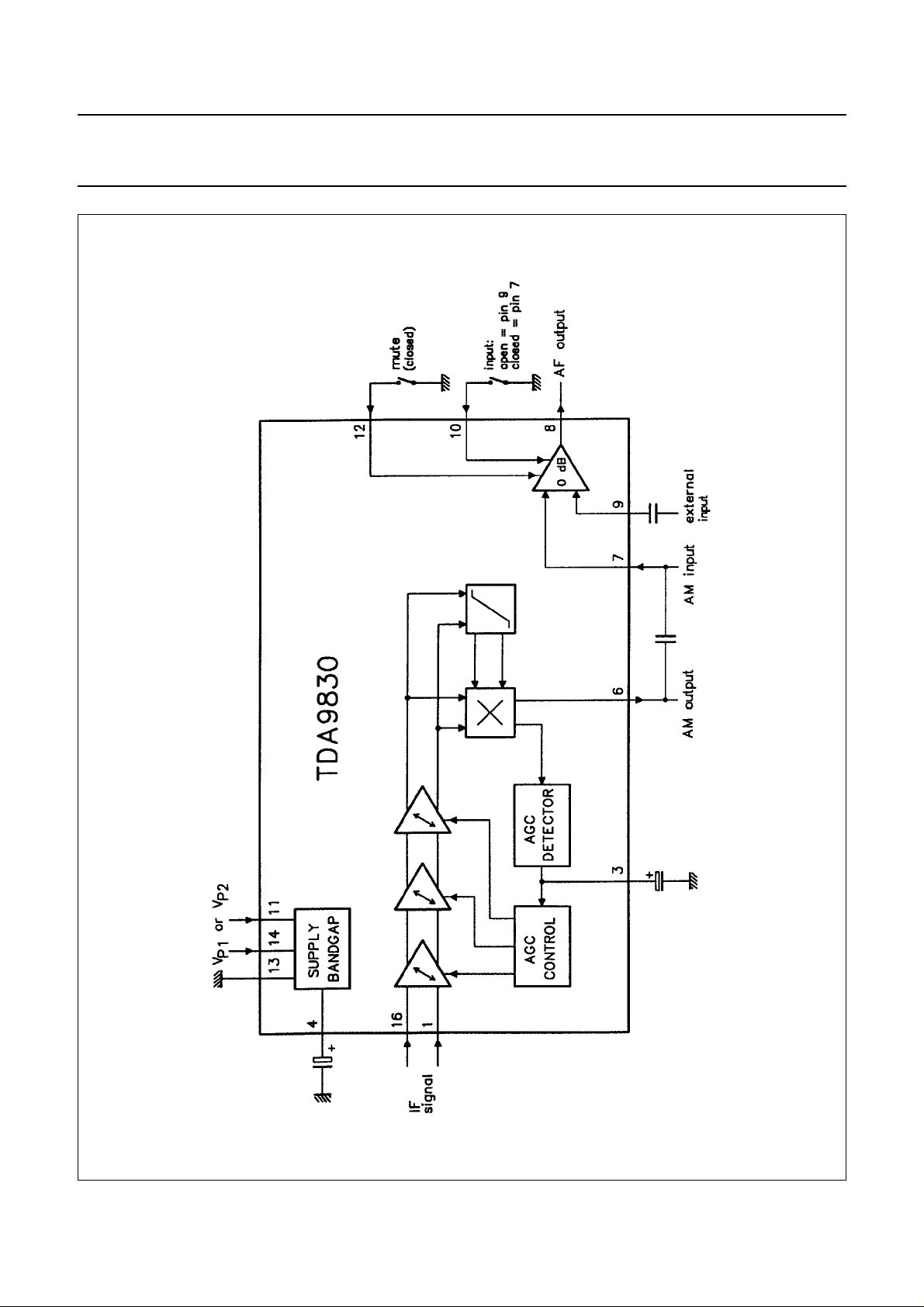
Fig.1 Block diagram.
Page 4
Philips Semiconductors Product specification
TV sound AM-demodulator and audio source switch TDA9830
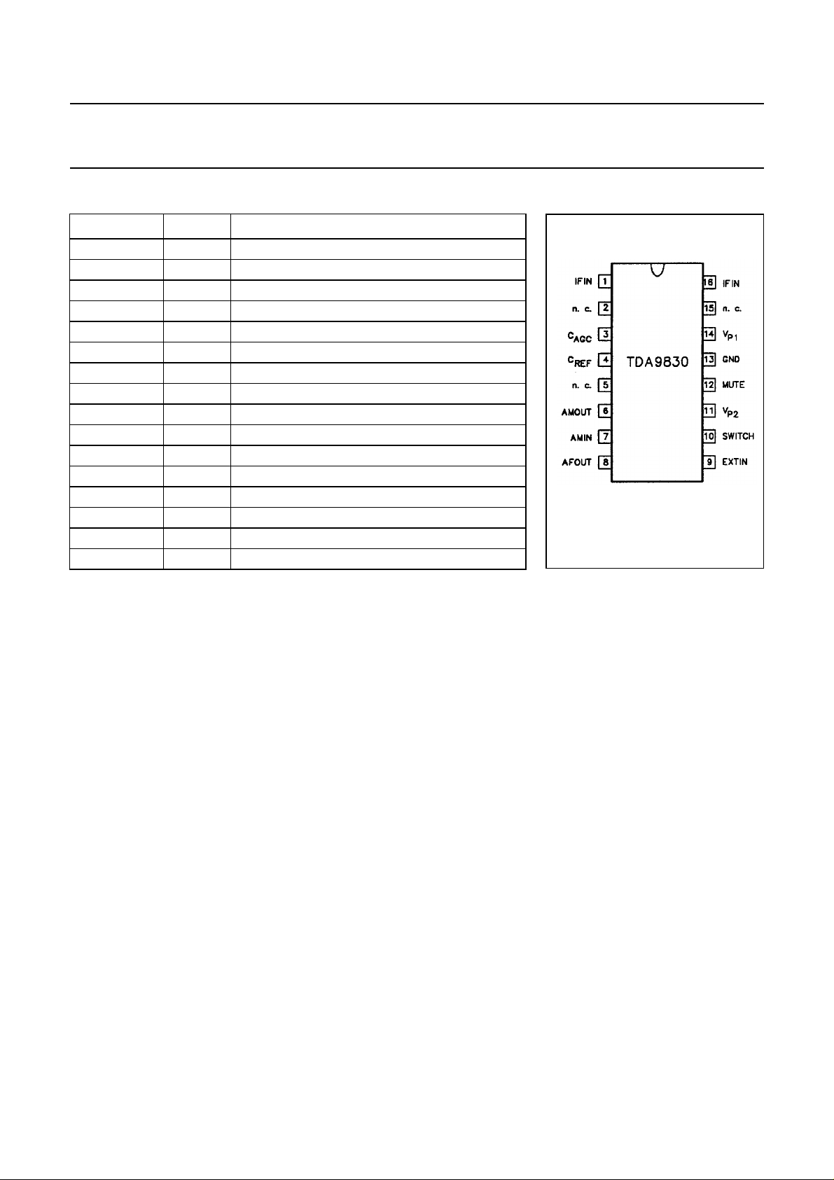
PINNING
SYMBOL PIN DESCRIPTION
IFIN 1 sound IF differential input signal
n.c. 2 not connected
C
AGC
C
REF
n.c. 5 not connected
AMOUT 6 AM demodulator output
AMIN 7 input signal (from AM) to audio switch
AFOUT 8 output signal from audio switch
EXTIN 9 input signal (from external) to audio switch
SWITCH 10 switch input select control
V
p2
MUTE 12 mute control
GND 13 ground (0 V)
V
p1
n.c. 15 not connected
IFIN 16 sound IF differential input signal
3 AGC capacitor
4 REF voltage filtering capacitor
11 supply voltage +12 V (alternative)
14 supply voltage +5 to +8 V
Fig.2 Pin configuration.
FUNCTIONAL DESCRIPTION
Sound IF input
The sound IF amplifier consists of
three AC-coupled differential
amplifier stages each with
approximately 20 dB gain. At the
output of each stage is a multiplier for
gain controlling (→ current
distribution gain control). The overall
control range is approximately −6 to
+60 dB and the frequency response
(−3 dB) of the IF amplifier is
approximately 6 to 70 MHz. The
steepness of gain control is
approximately 10 mV/dB.
IF AGC
The automatic gain control voltage to
maintain the AM demodulator output
signal at a constant level is generated
by a mean level detector. This
AGC-detector charges and
discharges the capacitor at pin 3
controlled by the output signal of the
AM-demodulator compared to an
internal reference voltage. The
maximum charge/discharge current is
approximately 5 µA. This value in
combination with the value of the
AGC capacitor and the AGC
steepness determines the lower
cut-off audio frequency and the
THD-figure at low modulation
frequency of the whole
AM-demodulator. Therefore a large
time constant has to be chosen which
leads to slow AGC reaction at IF level
change. To speed up the AGC in case
of IF signal jump from low to high
level, there is an additional
comparator built in, which can provide
additional discharge current from the
AGC capacitor up to 5 mA in a case of
overloading the AM demodulator by
the internal IF signal.
AM-demodulator
The IF amplifier output signal is fed to
a limiting amplifier (two stages) and to
a multiplier circuit. However the limiter
output signal (which is not any more
AM modulated) is also fed to the
multiplier, which provides AM
demodulation (in phase
demodulation). After lowpass filtering
≈ 400 kHz) for carrier rejection and
(f
g
buffering, the demodulator output
signal is present at pin 6. The AM
demodulator operates over a wide
frequency range, so that in
combination with the frequency
response of the IF amplifier
applications in a frequency range
from approximately 6 MHz up to
70 MHz are possible.
Audio switch
This circuit is an operational amplifier
with three input stages and internal
feedback network determining gain
(0 dB) and frequency response
(f
≈ 700 kHz). Two of the input
g
stages are connected to pin 7 and pin
9, the third input stage to an internal
reference voltage. Controlled by the
switching pins 10 and 12, one of the
three input stages can be activated
and a choice made between two
different AF signals or mute state.
The selected signal is present at
June 1994 4
Page 5
Philips Semiconductors Product specification
TV sound AM-demodulator and audio source switch TDA9830
pin 8. The decoupling capacitors at
the input pins are needed, because
the internally generated bias voltage
for the input stages must not be
influenced by the application in order
to avoid DC-plop in case of switching.
The AM demodulator output is
designed to provide almost the same
DC voltage as the input bias voltage
of the audio switch. But there may be
spread between both voltages.
Therefore it is possible to connect pin
6 directly to pin 7 (without a
decoupling capacitor), but in this
event the DC-plop for switching can
increase up to 100 mV.
Reference circuit
This circuit is a band gap stabilizer in
combination with a voltage regulation
amplifier, which provides an internal
reference voltage of about 3.6 V
nearly independent from supply
voltage and temperature. This
reference voltage is filtered by the
capacitor at pin 4 in order to reduce
noise. It is used as a reference to
generate all important voltages and
currents of the circuit.
For application in 12 V power supply
concepts, there is an internal voltage
divider in combination with a
Darlington transistor in order to
reduce the supply voltage for all IC
function blocks to approximately 6 V.
This is necessary because of use of
modern high frequency IC
technology, where most of the used
integrated components are only
allowed to operate at maximum 9 V
supply voltage.
LIMITING VALUES
In accordance with the Absolute Maximum Rating System (IEC134).
SYMBOL PARAMETER MIN. MAX. UNIT
V
14−13
V
11−13
V
10, 12−13
T
amb
T
stg
supply voltage V
supply voltage V
P1
P2
−0.5 +8.9 V
−0.5 +13.3 V
switching voltage −0.5 VP+ 0.5 V
operating ambient temperature 0 +70 °C
storage temperature −25 +150 °C
Note to the limiting values
1. To avoid an inadmissible increase of ambient temperature, it is not allowed to short-circuit pin 11 for more than 10
seconds to ground.
THERMAL RESISTANCE
SYMBOL PARAMETER THERMAL RESISTANCE
R
th j-a
from junction to ambient in free air
SOT38 74 K/W
SOT109 100 K/W
June 1994 5
Page 6

Philips Semiconductors Product specification
TV sound AM-demodulator and audio source switch TDA9830
CHARACTERISTICS
= 5.0 V at pin 14; T
V
P1
m = 54%. IF input signal (sound carrier): V
SYMBOL PARAMETER CONDITIONS MIN. TYP. MAX. UNIT
V
14−13
V
11−13
I
11/I14
positive supply voltage V
positive supply voltage V
current consumption 24 30 36 mA
IF amplifier and gain control
R
C
V
V
G
I
1−16
1−16
1−16
1−16
v
3
input resistance 1.75 2.2 2.65 kΩ
input capacitance 1.0 1.5 2.2 pF
minimum IF input signal (RMS value) note 2 − 60 100 µV
maximum IF input signal (RMS value) note 3 70 120 − mV
gain control 60 66 − dB
maximum AGC charging/discharging
current
I
3
V
−V13gain control voltage (G
3
fast AGC discharging current −−5mA
B −3 dB IF bandwidth upper cut-off
V
1/16−13
DC potential − 1.7 − V
AM-Demodulator
V
6−13
AF output signal (RMS value) 400 500 600 mV
B −3 dB AF bandwidth upper cut-off
V
V
V
R
6−13
6−13
6−13
6
THD − 0.8 2 %
S/N (weighted acc. CCIR 468-3) 47 53 − dB
DC potential 2.00 2.15 2.30 V
output resistance
(emitter follower with 0.5 mA bias current)
I
6abs
I
6
allowable AC output current −−0.3 mA
allowable DC output current −−−0.5 mA
Audio-switch
V
7,9−13
AF-input-signal for THD < 1.5%
(RMS value)
V
8−13
S/N ratio of audio switch
(in accordance with CCIR 468-3)
B −3 dB AF bandwidth upper limit 100 −−kHz
V
8−13
THD at 1 V
= +25 °C; sound carrier fSC= 32.4 MHz modulated with f = 1 kHz and modulation depth
amb
P1
P2
1-16
10 mV
; unless otherwise specified.
RMS
note 1 4.5 5.0 8.8 V
note 1 10.8 12.0 13.2 V
3.5 5 7 µA
− G
min
) 1.5 − 2.8 V
max
50 70 − MHz
frequency
lower cut-off
− 6 10 MHz
frequency
100 −−kHz
frequency
lower cut-off
−−20 Hz
frequency; note 7
− 300 −Ω
−−1.2 V
reference signal
70 80 − dB
at pin 7/9 is
0.5 V
RMS
input signal at pin 7 or 9 − 0.1 1.0 %
RMS
June 1994 6
Page 7

Philips Semiconductors Product specification
TV sound AM-demodulator and audio source switch TDA9830
SYMBOL PARAMETER CONDITIONS MIN. TYP. MAX. UNIT
V
8−13
V
7,8,9−13
R
7,9−13
G
7,9−8
V
10−13
V
10−13
V
12−13
I
10, 12
V
8-13
R
8
Ripple rejection note 6
RR AF signal output:
crosstalk and mute attenuation 20 Hz to 20 kHz 80 90 − dB
DC-potential 2.00 2.15 2.30 V
input resistance 40 50 60 kΩ
gain of audio switch −0.5 0 +0.5 dB
audio switching voltage to activate pin 7 0 − 0.8 V
audio switching voltage to activate pin 9 note 4 1.5 − V
P
V
input voltage for MUTE-ON 0 − 0.8 V
input voltage for MUTE-OFF note 4 1.5 − V
output current of switching-pins at
V
10, 12-13
= 0 V
DC-plop at AF output pin with switching
note 5 − 510mV
−110 −145 −185 µA
P
V
from internal to external audio signal or
to mute-state or vice-versa
output resistance 70 100 150 Ω
26 30 − dB
αRR=V
AF signal output with AF signal from
ripple
on VP/V
ripple
on V
out
40 44 − dB
external source
Notes to the characteristics
1. In the power supply voltage range VP1= 5.0 V up to 8.0 V the performance will not change essentially.
With power supply from VP2= 12.0 V the performance will be comparable with the performance at VP1= 5.0 V up to
8.0 V.
The unused power supply pin must be not connected.
2. Start of gain control (low IF input signal) at −3 dB AF signal reduction at pin 6.
3. End of gain control (high IF input signal) at +1 dB AF signal expansion at pin 6.
4. This state is also valid for pin left open-circuit.
5. If a DC-plop of about maximum 100 mV is acceptable when switching from internal to external audio-signal or from
internal to mute state or vice versa, the capacitor between pin 6 and 7 can be omitted and pin 6 can be connected
to pin 7.
6. Measured with V
ripple
= 200 mV
at 70 Hz superimposed on supply voltage VP.
(p-p)
7. Dependent on value of AGC capacitor.
June 1994 7
Page 8

Philips Semiconductors Product specification
TV sound AM-demodulator and audio
source switch
TDA9830
June 1994 8
Fig.3 Internal circuits.
Page 9
Philips Semiconductors Product specification
TV sound AM-demodulator and audio source switch TDA9830
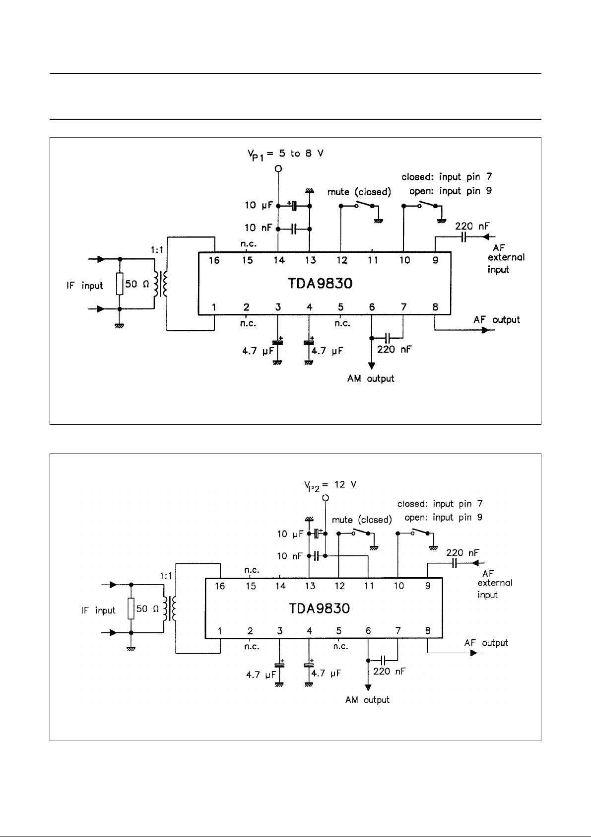
Fig.4 Test circuit 5 to 8 V supply.
Fig.5 Test circuit 12 V supply.
June 1994 9
Page 10

Philips Semiconductors Product specification
TV sound AM-demodulator and audio source switch TDA9830
Fig.6 S/N figure as a function of the IF input signal.
Fig.7 Frequency response at pin 6.
Fig.8 THD at pin 6.
June 1994 10
Page 11

June 1994 11
Philips Semiconductors Product specification
TV sound AM-demodulator and audio
source switch
Fig.9 Proposed tolerance scheme IF filter for standard L.
With an IF filter according to this proposal, the video buzz suppression on the audio output is better than 50 dB (in accordance with CCIR468−3,
m = 54%) for the worst case video modulation with 6 kHz sinewave black-to-white.
TDA9830
Page 12
Philips Semiconductors Product specification
TV sound AM-demodulator and audio source switch TDA9830
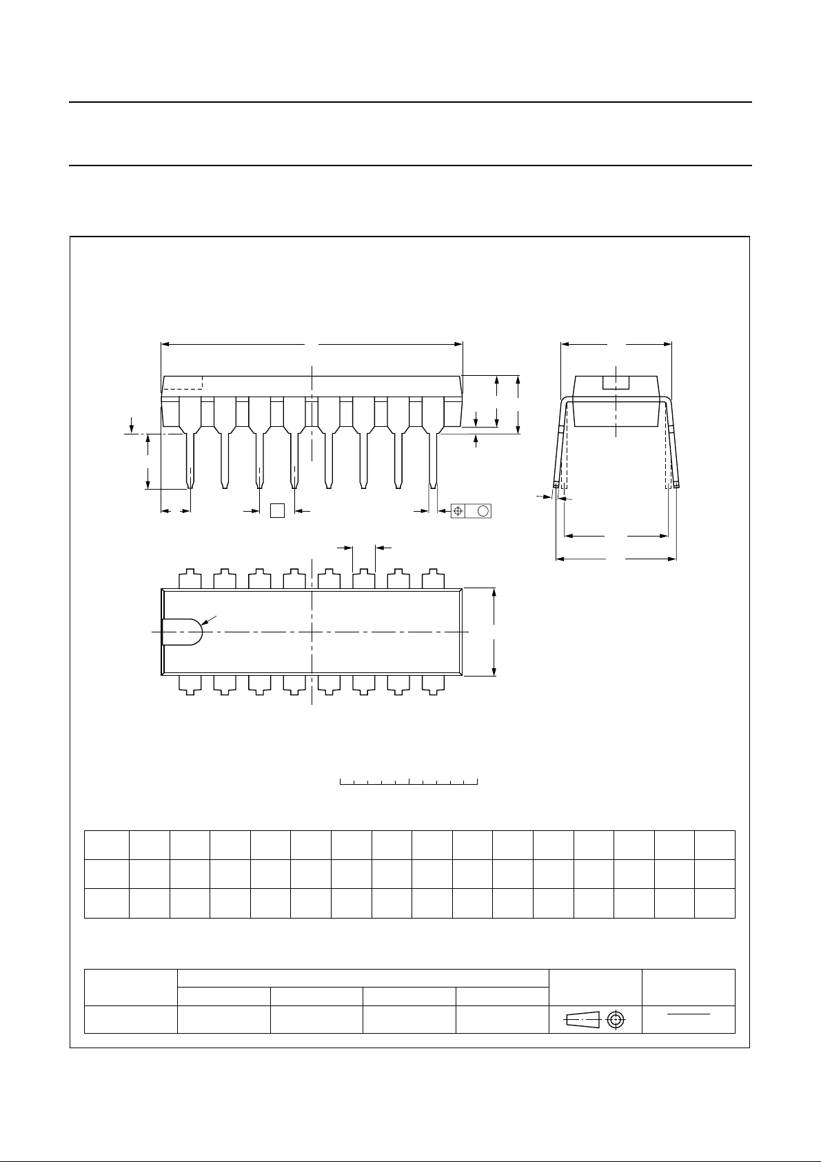
PACKAGE OUTLINES
DIP16: plastic dual in-line package; 16 leads (300 mil); long body
D
seating plane
L
Z
16
pin 1 index
e
b
b
1
9
A
1
w M
SOT38-1
M
E
A
2
A
c
(e )
1
M
H
E
1
0 5 10 mm
scale
DIMENSIONS (inch dimensions are derived from the original mm dimensions)
A
UNIT
mm
inches
Note
1. Plastic or metal protrusions of 0.25 mm maximum per side are not included.
A
max.
4.7 0.51 3.7
OUTLINE
VERSION
SOT38-1
min.
A
1 2
max.
0.15
IEC JEDEC EIAJ
050G09 MO-001AE
b
1.40
1.14
0.055
0.045
b
0.53
0.38
0.021
0.015
1
cEe M
0.32
0.23
0.013
0.009
REFERENCES
(1) (1)
D
21.8
21.4
0.86
0.84
June 1994 12
8
6.48
6.20
0.26
0.24
e
0.30
1
0.15
0.13
M
L
3.9
3.4
E
8.25
7.80
0.32
0.31
EUROPEAN
PROJECTION
H
9.5
0.2542.54 7.62
8.3
0.37
0.010.100.0200.19
0.33
ISSUE DATE
w
92-10-02
95-01-19
Z
max.
2.2
0.087
(1)
Page 13
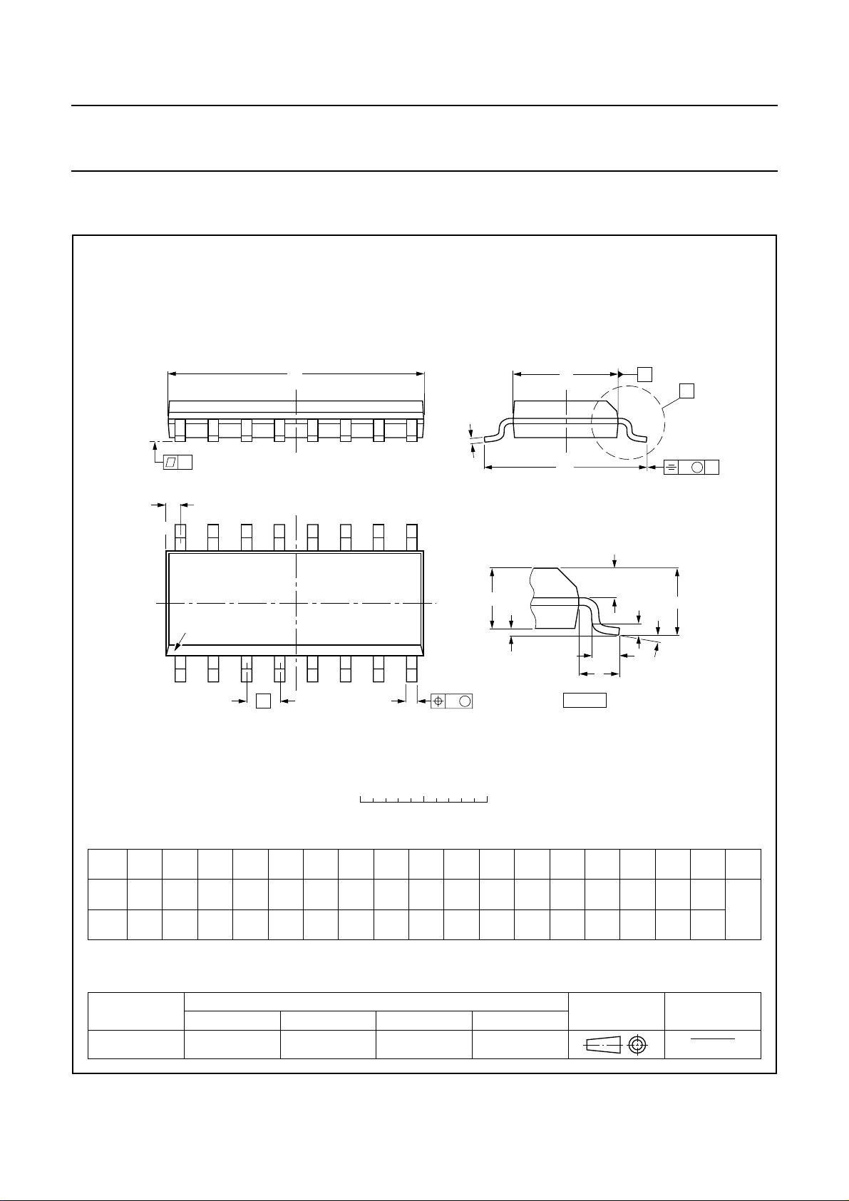
Philips Semiconductors Product specification
TV sound AM-demodulator and audio source switch TDA9830
SO16: plastic small outline package; 16 leads; body width 3.9 mm
D
c
y
Z
16
pin 1 index
1
e
9
8
b
w M
p
SOT109-1
E
H
E
A
2
A
1
L
detail X
A
X
v M
A
Q
(A )
L
p
A
3
θ
0 2.5 5 mm
scale
DIMENSIONS (inch dimensions are derived from the original mm dimensions)
mm
OUTLINE
VERSION
SOT109-1
A
max.
1.75
0.069
A1A2A
0.25
1.45
0.10
1.25
0.010
0.057
0.004
0.049
3
0.25
0.01
IEC JEDEC EIAJ
076E07S MS-012AC
b
p
0.49
0.36
0.019
0.014
0.25
0.19
0.0100
0.0075
UNIT
inches
Note
1. Plastic or metal protrusions of 0.15 mm maximum per side are not included.
(1)E(1) (1)
cD
10.0
4.0
3.8
0.16
0.15
1.27
0.050
9.8
0.39
0.38
REFERENCES
June 1994 13
eHELLpQZywv θ
1.05
0.041
1.0
0.4
0.039
0.016
0.7
0.25
0.6
0.028
0.01 0.004
0.020
EUROPEAN
PROJECTION
0.25 0.1
0.01
0.7
0.3
0.028
0.012
ISSUE DATE
95-01-23
97-05-22
o
8
o
0
6.2
5.8
0.244
0.228
Page 14

Philips Semiconductors Product specification
TV sound AM-demodulator and audio source switch TDA9830
SOLDERING
Introduction
There is no soldering method that is ideal for all IC
packages. Wave soldering is often preferred when
through-hole and surface mounted components are mixed
on one printed-circuit board. However, wave soldering is
not always suitable for surface mounted ICs, or for
printed-circuits with high population densities. In these
situations reflow soldering is often used.
This text gives a very brief insight to a complex technology.
A more in-depth account of soldering ICs can be found in
“IC Package Databook”
our
(order code 9398 652 90011).
DIP
SOLDERING BY DIPPING OR BY WAVE
The maximum permissible temperature of the solder is
260 °C; solder at this temperature must not be in contact
with the joint for more than 5 seconds. The total contact
time of successive solder waves must not exceed
5 seconds.
The device may be mounted up to the seating plane, but
the temperature of the plastic body must not exceed the
specified maximum storage temperature (T
stg max
). If the
printed-circuit board has been pre-heated, forced cooling
may be necessary immediately after soldering to keep the
temperature within the permissible limit.
R
EPAIRING SOLDERED JOINTS
Apply a low voltage soldering iron (less than 24 V) to the
lead(s) of the package, below the seating plane or not
more than 2 mm above it. If the temperature of the
soldering iron bit is less than 300 °C it may remain in
contact for up to 10 seconds. If the bit temperature is
between 300 and 400 °C, contact may be up to 5 seconds.
to the printed-circuit board by screen printing, stencilling or
pressure-syringe dispensing before package placement.
Several techniques exist for reflowing; for example,
thermal conduction by heated belt. Dwell times vary
between 50 and 300 seconds depending on heating
method. Typical reflow temperatures range from
215 to 250 °C.
Preheating is necessary to dry the paste and evaporate
the binding agent. Preheating duration: 45 minutes at
45 °C.
W
AVE SOLDERING
Wave soldering techniques can be used for all SO
packages if the following conditions are observed:
• A double-wave (a turbulent wave with high upward
pressure followed by a smooth laminar wave) soldering
technique should be used.
• The longitudinal axis of the package footprint must be
parallel to the solder flow.
• The package footprint must incorporate solder thieves at
the downstream end.
During placement and before soldering, the package must
be fixed with a droplet of adhesive. The adhesive can be
applied by screen printing, pin transfer or syringe
dispensing. The package can be soldered after the
adhesive is cured.
Maximum permissible solder temperature is 260 °C, and
maximum duration of package immersion in solder is
10 seconds, if cooled to less than 150 °C within
6 seconds. Typical dwell time is 4 seconds at 250 °C.
A mildly-activated flux will eliminate the need for removal
of corrosive residues in most applications.
EPAIRING SOLDERED JOINTS
R
SO
REFLOW SOLDERING
Reflow soldering techniques are suitable for all SO
packages.
Reflow soldering requires solder paste (a suspension of
fine solder particles, flux and binding agent) to be applied
June 1994 14
Fix the component by first soldering two diagonallyopposite end leads. Use only a low voltage soldering iron
(less than 24 V) applied to the flat part of the lead. Contact
time must be limited to 10 seconds at up to 300 °C. When
using a dedicated tool, all other leads can be soldered in
one operation within 2 to 5 seconds between
270 and 320 °C.
Page 15

Philips Semiconductors Product specification
TV sound AM-demodulator and audio source switch TDA9830
DEFINITIONS
Data sheet status
Objective specification This data sheet contains target or goal specifications for product development.
Preliminary specification This data sheet contains preliminary data; supplementary data may be published later.
Product specification This data sheet contains final product specifications.
Limiting values
Limiting values given are in accordance with the Absolute Maximum Rating System (IEC 134). Stress above one or
more of the limiting values may cause permanent damage to the device. These are stress ratings only and operation
of the device at these or at any other conditions above those given in the Characteristics sections of the specification
is not implied. Exposure to limiting values for extended periods may affect device reliability.
Application information
Where application information is given, it is advisory and does not form part of the specification.
LIFE SUPPORT APPLICATIONS
These products are not designed for use in life support appliances, devices, or systems where malfunction of these
products can reasonably be expected to result in personal injury. Philips customers using or selling these products for
use in such applications do so at their own risk and agree to fully indemnify Philips for any damages resulting from such
improper use or sale.
June 1994 15
 Loading...