

Page 1

INTEGRATED CIRCUITS
DATA SH EET
TDA9829T
Downconverter for DVB
Product specification
File under Integrated Circuits, IC02
1998 Nov 09
Page 2

Philips Semiconductors Product specification
Downconverter for DVB TDA9829T
FEATURES
• 5 V supply voltage
• Gain controlled IF-amplifier
GENERAL DESCRIPTION
The TDA9829T is an integrated circuit for DVB-IF
processing.
• Mixer for DVB-IF downconversion
• VCO for Quadrature Amplitude Modulation (QAM)
carrier recovery
• External VCO control
• Internal and external AGC
• DVB output level adjust via AGC adjust
• High level DVB operational output amplifier
• Mute switch for DVB output
• Tuner AGC with adjustable takeover point (TOP)
• AFC detector without extra reference circuit
• Stabilizer circuit for ripple rejection and to achieve
constant output signals.
QUICK REFERENCE DATA
SYMBOL PARAMETER CONDITIONS MIN. TYP. MAX. UNIT
V
P
I
P
V
3-4(rms)
∆ϕ
SSB
α
mute
I
12(sink)
supply voltage note 1 4.5 5.0 5.5 V
supply current 81 96 111 mA
input sensitivity (RMS value) −1 dB DVB signal at output − 100 150 µV
VCO phase noise f = 100 kHz; free-running 103 107 − dBc/Hz
mute attenuation note 2 − 36 − dB
sink current maximum tuner gain
1.5 2 2.6 mA
reduction; see Fig.3
CR
stps(US)
V
11(p-p)
B
−1dB
α
H
PSRR power supply ripple rejection at
control steepness ∆I14/∆fIF for
USA
output voltage
(peak-to-peak value)
fIF= 43.75 MHz;
notes 3 and 4; see Fig.4
CL< 15 pF; RL>5kΩ; with
internal AGC
0.7 0.98 1.3 µA/kHz
1.8 2.1 2.4 V
−1 dB bandwidth CL< 15 pF; RL>5kΩ 11 12 − MHz
suppression of in-band harmonics Vo= 2.0 V (p-p) 30 35 − dB
see Fig.5 26 36 − dB
pin 11
Notes
1. Performance may be decreased at V
= 4.5 V.
P
2. This parameter is not tested during production and is only given as application information for designing the television
receiver.
3. To match the AFC output signal to different tuning systems a current source output is provided. The test circuit is
given in Fig.4. The AFC-steepness can be changed by the resistors at pin 14.
4. Depending on the ratio ∆C/C0 of the LC resonant circuit of VCO (Q0> 50; C0=C
int+Cext
; see Table 2).
1998 Nov 09 2
Page 3
Philips Semiconductors Product specification
Downconverter for DVB TDA9829T
ORDERING INFORMATION
TYPE
NUMBER
NAME DESCRIPTION VERSION
PACKAGE
TDA9829T SO20 plastic small outline package; 20 leads; body width 7.5 mm SOT163-1
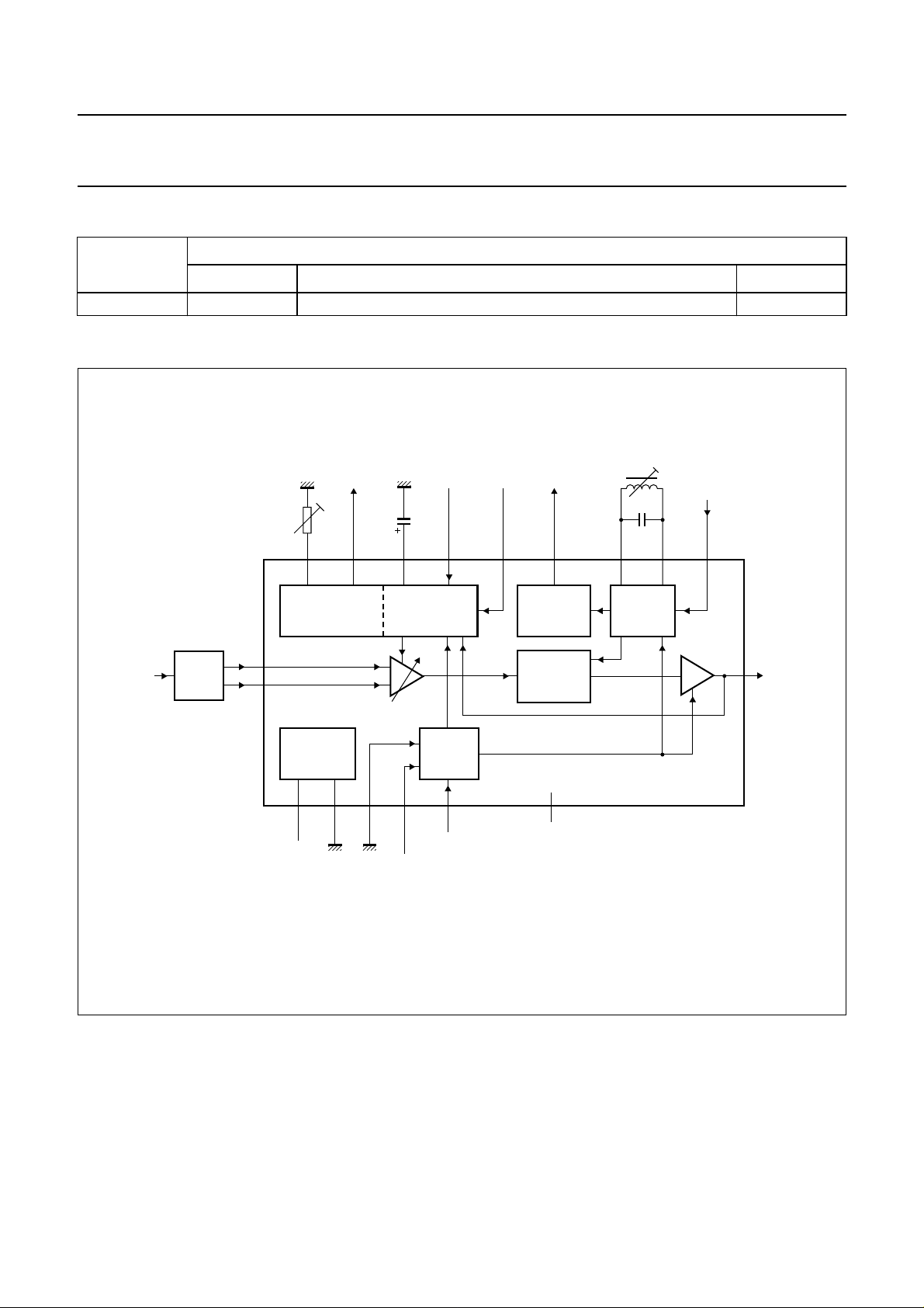
BLOCK DIAGRAM
15
DVB
external
VCO
control
V
10
VCO
11
V
oDVB
2 V (p-p)
handbook, full pagewidth
DVB-IF
input
DVB
IF filter
DVB
C
C
18125
AGC
adjust
AGC
AGC VCO1AFC VCO2TAGC
DVB
AGC
tuner
AGC
TOP
TADJ
TUNER
AGC
V
iIF1
3
4
V
iIF2
DVB
AGC
external
V
AGCAGCADJ
9
8
14
AFC
DETECTOR
DVB
MIXER
2 × f
PC
16
VCO
TWD
INTERNAL
VOLTAGE
STABILIZER
19 17 1 20 6
VPGND
+5 V
V
SID
MUTESWI
Fig.1 Block diagram.
LOGIC
AGCSWI
2, 7, 13
n.c.
TDA9829T
MHB219
1998 Nov 09 3
Page 4
Philips Semiconductors Product specification
Downconverter for DVB TDA9829T
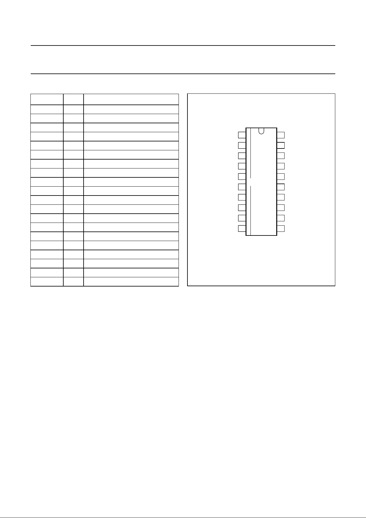
PINNING
SYMBOL PIN DESCRIPTION
V
SID
n.c. 2 not connected
V
iIF1
V
iIF2
TADJ 5 tuner AGC takeover adjust (TOP)
AGCSWI 6 AGC switch input
n.c. 7 not connected
V
AGC
AGCADJ 9 AGC adjust input
V
VCO
V
oDVB
TAGC 12 tuner AGC output
n.c. 13 not connected
AFC 14 AFC output
VCO1 15 VCO1 reference circuit
VCO2 16 VCO2 reference circuit
GND 17 ground
C
AGC
V
P
MUTESWI 20 mute switch input
1 SIF down input
3 IF differential input signal voltage 1
4 IF differential input signal voltage 2
8 AGC voltage input
10 VCO control voltage
11 DVB output
18 AGC capacitor
19 supply voltage (+5 V)
handbook, halfpage
V
1
SID
2
n.c.
V
3
iIF1
V
4
iIF2
TADJ
5
TDA9829T
V
V
n.c.
AGC
VCO
6
7
8
9
10
AGCSWI
AGCADJ
Fig.2 Pin configuration.
MHB220
20
19
18
17
16
15
14
13
12
11
MUTESWI
V
P
C
AGC
GND
VCO2
VCO1
AFC
n.c.
TAGC
V
oDVB
1998 Nov 09 4
Page 5

Philips Semiconductors Product specification
Downconverter for DVB TDA9829T
FUNCTIONAL DESCRIPTION
Vision IF amplifier
The vision IF amplifier consists of three AC-coupled
differential amplifier stages. Each differential stage
comprises a feedback network controlled by emitter
degeneration to control the IF gain.
VCO, Travelling Wave Divider (TWD) and AFC
The VCO operates with a resonance circuit (with L and C
in parallel) at double the IF frequency plus symbol
frequency. The VCO is controlled by integrated variable
capacitors. The control voltage required to tune the VCO
from its free-running frequency to its actual frequency is
fed to the capacitors. This control voltage is amplified and
converted into a current which represents the AFC output
signal. At centre frequency the AFC output current is equal
to zero.
The oscillator signal is divided-by-two with a TWD which
generates a differential output signal for downconverting
the IF signal.
DVB mixer
The gain controlled DVB-IF signal is downconverted to the
symbol frequency by use of a four quadrant multiplier.
The conversion signal is provided by the VCO and TWD.
DVB AGC and tuner AGC
The AGC detector charges/discharges the AGC capacitor
to the required voltage for setting the IF and tuner gain in
order to keep the DVB signal at a constant level.
A peak detector is used for the DVB AGC. The peak value
of (digital) the QAM signal is detected and controlled to a
constant value by the variable gain IF amplifier.
The detector bandwidth is adapted to the symbol
frequency (3 to 11 MHz). The external AGC time constant
is given by the IF AGC capacitor at pin 18.
The AGC capacitor voltage is transferred to an internal IF
control signal, and is fed to the tuner AGC to generate the
tuner AGC output current (open-collector output).
The tuner AGC takeover point can be adjusted. This
allows the tuner and the SWIF filter to be matched to
achieve the optimum IF input level.
The DVB output signal (V
of ±3 dB by a control voltage (∆V
) can be adjusted in a range
oDVB
) at pin 9. The internal
adj
AGC can be switched off at pin 6 and the IF gain can be
controlled by an external voltage at pin 8. The tuner AGC
is active in both instances.
DVB output amplifier
The output amplifier for the DVB signal has a high
bandwidth and delivers a 2 V (p-p) signal. The amplifier
can be switched to a mute state forced by the signal at
pin 20.
Internal voltage stabilizer
A band gap circuit internally generates a voltage of
approximately 1.25 V, independent of supply voltage and
temperature. A voltage regulator circuit, connected to this
voltage, produces a constant voltage of 3.6 V which is
used as an internal reference voltage.
LIMITING VALUES
In accordance with the Absolute Maximum Rating System (IEC 134).
SYMBOL PARAMETER CONDITIONS MIN. MAX. UNIT
V
P
V
n
supply voltage (pin 19) maximum chip temperature of 125 °C 0 5.5 V
voltage at pins
0V
P
1 to 10, 13, 14 and 18 to 20
t
sc(max)
V
12
T
stg
T
amb
V
es
maximum short-circuit time − 10 s
tuner AGC output voltage 0 13.2 V
storage temperature −25 +150 °C
operating ambient temperature −20 +70 °C
electrostatic handling voltage machine model class B −300 +300 V
1998 Nov 09 5
V
Page 6
Philips Semiconductors Product specification
Downconverter for DVB TDA9829T
THERMAL CHARACTERISTICS
SYMBOL PARAMETER CONDITIONS VALUE UNIT
R
th(j-a)
thermal resistance from junction
to ambient
CHARACTERISTICS
=5V; T
V
P
=25°C; see Table 1 for input frequencies; input level V
amb
taken in Fig.8; unless otherwise specified.
SYMBOL PARAMETER CONDITIONS MIN. TYP. MAX. UNIT
Supply (pin 19)
V
P
I
P
IF amplifier (measured at f
∆V
(3-4)(rms)
V
i(3-4)(rms)
supply voltage note 1 4.5 5.0 5.5 V
supply current 81 96 111 mA
= 43.75 MHz; pins 3 and 4)
IF
input sensitivity (RMS value) −1 dB DVB signal at output − 100 150 µV
maximum input signal level
(RMS value)
∆G
IF
total gain control IF amplifier 59 64 − dB
tilt for ∆f ±3 MHz f
R
i(3-4)(diff)
C
i(3-4)(diff)
input resistance (differential) note 2 − 2.2 − kΩ
input capacitance (differential) note 2 − 1.7 − pF
DVB mixer and VCO (pins 10, 15 and 16); see notes 4 and 5 and Table 1
f
VCO(max)
f
VCO(US)
f
VCO(EU)
V
ref(rms)
maximum oscillator frequency 2(fIF+fs) 125 130 − MHz
VCO frequency for USA 2(fIF+fs) − 97.5 − MHz
VCO frequency for Europe 2(fIF+fs) − 86.0 − MHz
oscillator voltage swing between
pins 15 and 16 (RMS value)
∆ϕ
V
R
VCO
SSB
i(VCO)
VCO phase noise f = 100 kHz; free-running 103 107 − dBc/Hz
VCO control range (pin 10) see Figs 6 and 7 0 − V
VCO control input resistance
(pin 10)
CR
stps(VCO)
control steepness ∆fs/∆V
10
in free air 85 K/W
= 10 mV (RMS value); measurements
iIF(3−4)
1 dB DVB signal at output 140 200 − mV
= 6.9 MHz; 40 dB gain − 0.5 1 dB
s
− 60 − mV
P
V
50 63 76 kΩ
see Figs 6 and 7
DVB (USA) − 0.29 − MHz/V
DVB (Europe) − 0.40 − MHz/V
DVB output amplifier (pins 11 and 20)
V
o(DVB)(p-p)
DVB output signal (QAM)
(peak-to-peak value)
I
bias(int)
DC internal bias current for
emitter-follower (pin 11)
I
sink(max)
maximum AC and DC output
sink current (pin 11)
I
source(max)
maximum AC and DC output
source current (pin 11)
1998 Nov 09 6
1.8 2.1 2.4 V
1.9 2.3 2.7 mA
1.5 −−mA
2.0 −−mA
Page 7

Philips Semiconductors Product specification
Downconverter for DVB TDA9829T
SYMBOL PARAMETER CONDITIONS MIN. TYP. MAX. UNIT
α
mute
V
i(mute)
I
IL
DVB AGC detector (pins 8, 9 and 18)
t
resp
I
ch
I
dch
∆V
i(AGC)
∆R
i(AGC)
∆AGC
stps
V
AGC(ext)
R
i(AGC)(ext)
mute attenuation note 2 − 36 − dB
mute switch input voltage
(pin 20)
DVB mute; note 3 1.3 − V
P
DVB no mute 0 − 0.8 V
V
LOW-level input current (pin 20) V20= 0 V 180 230 280 µA
response to an increasing
note 6 − 0.25 − ms/dB
amplitude step in the IF input
signal
response to a decreasing
note 6 − 0.25 − ms/dB
amplitude step in the IF input
signal
charging current (pin 18) − 200 −µA
discharging current (pin 18) − 200 −µA
AGC adjust input voltage range
1 2.5 4.5 V
(pin 9)
AGC adjust input resistance
8 1012kΩ
(pin 9)
AGC adjust steepness 2 V < V9<3V −−5−dB/V
external AGC voltage for DVB
see Fig.3 1 − 4.5 V
(pin 8)
external AGC input resistance
40 −−kΩ
(pin 8)
Tuner AGC (pin 12)
V
i(min)(rms)
IF input signal voltage for
minimum starting point of tuner
takeover (RMS value)
V
i(max)(rms)
IF input signal voltage for
maximum starting point of tuner
takeover (RMS value)
V
o
V
sat
V∆
TOP 12,
----------------------- T∆
I
sink
permissible output voltage from external source; note 2 −−13.2 V
saturation voltage I
variation of takeover point by
temperature
sink current see Fig.3
input at pins 3 and 4;
R
=22kΩ;
TOP
I
= 0.4 mA
TAGC
input at pins 3 and 4;
R
=0Ω; I
TOP
= 1.5 mA −−0.2 V
TAGC
I
= 0.4 mA − 0.03 0.07 dB/K
TAGC
TAGC
= 0.4 mA
no tuner gain reduction;
V
= 13.2 V
TAGC
maximum tuner gain
− 25mV
50 100 − mV
−−5µA
1.5 2 2.6 mA
reduction
1998 Nov 09 7
Page 8

Philips Semiconductors Product specification
Downconverter for DVB TDA9829T
SYMBOL PARAMETER CONDITIONS MIN. TYP. MAX. UNIT
∆G
IF
AFC circuit (pin 14); see notes 7 and 8 and Fig.4
CR
stps(US)
CR
stps(EU)
DVB output signal (IF input to DVB output)
V
o(p-p)
V
O(DC)
B
−1dB
B
−3dB
α
C(DVB)
α
H
PSRR power supply ripple rejection at
IF slip by automatic gain control tuner gain current from
− 68dB
20 to 80%
control steepness ∆I14/∆fIF for
fIF= 43.75 MHz 0.7 0.98 1.3 µA/kHz
USA
control steepness ∆I14/∆fIF for
fIF= 36.15 MHz 0.45 0.70 0.95 µA/kHz
Europe
output voltage (pin 11)
(peak-to-peak value)
CL< 15 pF; RL>5kΩ; with
internal AGC
1.8 2.1 2.4 V
DC output voltage − 2.5 − V
−1 dB bandwidth CL< 15 pF; RL>5kΩ 11 12 − MHz
−3 dB bandwidth − 17 − MHz
fundamental input signal and
35 40 − dB
IF harmonics
suppression of in-band
Vo= 2.0 V (p-p) 30 35 − dB
harmonics
see Fig.5 26 36 − dB
pin 11
Notes
1. Performance may be decreased at VP= 4.5 V.
2. This parameter is not tested during production and is only given as application information for designing the television
receiver.
3. Mute state also can be achieved by leaving pin 20 open-circuit.
4. Resonance circuit of VCO: Q0> 50; C
, C
and L see Table 2.
ext
int
5. Temperature coefficient of external LC-circuit is equal to zero.
6. Response speed valid for an IF input level range of 200 µVupto70mV.
7. To match the AFC output signal to different tuning systems a current source output is provided. The test circuit is
given in Fig.4. The AFC steepness can be changed by the resistors at pin 14.
8. Depending on the ratio ∆C/C0 of the LC resonant circuit of VCO (Q0> 50; C0=C
int+Cext
; see Table 2).
Table 1 Input frequencies, symbol frequencies and VCO frequencies
SYMBOL DESCRIPTION DVB (Europe) DVB (USA) UNIT
f
s
f
IF
f
VCO
Symbol frequency 6.9 5.0 MHz
IF frequency 36.15 43.75 MHz
VCO frequency 86.0 97.5 MHz
1998 Nov 09 8
Page 9

Philips Semiconductors Product specification
Downconverter for DVB TDA9829T
andbook, full pagewidth
(mV RMS)
(1) I
(2) Gain.
0.06
IF input
0.6
60
tuner
; R
TOP
gain
(dB)
70
60
50
40
30
206
10
0
−10
1 2.521.5 3 3.5 4
=22kΩ.
(3) I
(4) I
tuner
tuner
; R
; R
TOP
TOP
=11kΩ.
=0Ω.
(1) (2) (3) (4)
Fig.3 Typical IF and tuner AGC characteristic.
V18 (V)
MHB221
4.5
I
tuner
(mA)
0
1
2
handbook, full pagewidth
P
TDA9829T
VP = 5 V V
22 kΩ
I
14
14
22 kΩ
Fig.4 Measurement conditions and typical AFC characteristic.
1998 Nov 09 9
I
V
14
(V)
4.5
3.5
2.5
1.5
0.5
14
(µA)
−200
−100
0
100
200
35.75
43.45
36.15
43.75
MHB222
(source current)
(sink current)
36.55
fIF (MHz)
44.05
Page 10

Philips Semiconductors Product specification
Downconverter for DVB TDA9829T
handbook, full pagewidth
100
handbook, full pagewidth
f
VCO
(MHz)
99
VP = 5 V
TDA9829T
VP = 5 V
Fig.5 Ripple rejection condition.
100 mV (f
ripple
t
MHB223
= 70 Hz)
MHA661
98
97.5
97
96
95
01 4
L1 = 115 nH and C1 = 15 pF.
Fig.6 VCO control characteristic for DVB (USA).
1998 Nov 09 10
32
5V10 (V)
Page 11

Philips Semiconductors Product specification
Downconverter for DVB TDA9829T
89
handbook, full pagewidth
f
VCO
(MHz)
88
87
86
85
84
83
L1 = 248 nH and C1 = 5.6 pF.
32
Fig.7 VCO control characteristic for DVB (Europe).
MHA662
5V10 (V)01 4
1998 Nov 09 11
Page 12

Philips Semiconductors Product specification
Downconverter for DVB TDA9829T
TEST CIRCUIT
DVB
22 kΩ
n.c.
tuner
AGC
output
2 V (p-p)
VP = 5 VAFC
10 µF
BC546
68 Ω
220 Ω
DVB output
75 Ω
handbook, full pagewidth
(a) no mute
(b) mute
mute switch
VP = 5 V
(b)(a)
C
AGC
2.2
µF
10 nF
22 kΩ
100
nF
L1
(1)
C1
20
19 18 17 16
15 14 13 12 11
TDA9829T
1
2
3
4
5678910
(b)
AGC
switch
n.c.
DVB
AGC external
DVB
AGC adjust
VCO
control
MHB224
DVB-IF input
(1) See Table 2.
51 Ω
n.c.
1
2
3
4
22
kΩ
TOP
(a) AGC internal
(b) AGC external
(a)
Fig.8 Test circuit.
Table 2 Test circuit values
PARAMETER Europe USA
IF frequency 36.15 MHz 43.75 MHz
VCO frequency 86.0 MHz 97.5 MHz
Oscillator circuit
lfpage
(1) C(VCO) = 8.2 pF.
(2) C1 = 5.6 pF.
(3) L1 = 248 nH.
15
(1) (2)
16
lfpage
(3)
MHB225
(1) C(VCO) = 8.2 pF.
(2) C1 = 15 pF.
(3) L1 = 115 nH.
15
(1) (2)
16
(3)
MHB225
Toko coil 5KM 369SNS - 2010Z 5KM 369SNS - 1647Z
Philips ceramic capacitor 2222 632 39478 2222 632 33129
1998 Nov 09 12
Page 13

Philips Semiconductors Product specification
Downconverter for DVB TDA9829T
INTERNAL PIN CONFIGURATIONS
handbook, halfpage
1
+
1.1 kΩ
Fig.9 Pin 1; V
SID
+
3
5
1.1 kΩ
kΩ
3.6 V
kΩ
handbook, halfpage
5
3.6 V
+
2.65 V
4
MHB226
.
Fig.10 Pin 3; V
1.1 kΩ
and pin 4; V
iIF1
iIF2
2.65 V
MHB227
.
handbook, halfpage
30 kΩ
20
kΩ
+
9 kΩ
5
1.9 V
MHB228
3.6 V
Fig.11 Pin 5; TADJ.
1998 Nov 09 13
handbook, halfpage
26 kΩ
+
6
MHB229
Fig.12 Pin 6; AGCSWI.
3.6 V
Page 14

Philips Semiconductors Product specification
Downconverter for DVB TDA9829T
handbook, halfpage
+
8
Fig.13 Pin 8; V
50 kΩ
AGC
.
MHB230
handbook, halfpage
+
9
1.6 kΩ
Fig.14 Pin 9; AGCADJ.
12 kΩ
10.1 kΩ
3.6 V
17.2 kΩ
MHB231
handbook, halfpage
+
+
10
50 kΩ 50 kΩ
12.5 kΩ
2.7 V
Fig.15 Pin 10; V
VCO
VCO
MHB232
5 µA
.
1998 Nov 09 14
handbook, halfpage
+
11
Fig.16 Pin 11; V
+
2.7 mA
5.1 kΩ
5.1 kΩ
oDVB
10 µA
MHB233
.
Page 15

Philips Semiconductors Product specification
Downconverter for DVB TDA9829T
handbook, halfpage
handbook, halfpage
+
+
handbook, halfpage
12
2.5 mA
Fig.17 Pin 12; TAGC.
+
MHB234
14
200 µA
1 kΩ 1 kΩ
MHB235
Fig.18 Pin 14; AFC.
15
420 Ω
+
16
420 Ω
MHB236
2.8 V
Fig.19 Pin 15; VCO1 and pin 16; VCO2.
1998 Nov 09 15
handbook, halfpage
GND
17
MHB237
Fig.20 Pin 17; GND.
Page 16

Philips Semiconductors Product specification
Downconverter for DVB TDA9829T
handbook, halfpage
+
+
18
50 kΩ
++
200 µA
200 µA
Fig.21 Pin 18; C
MHB238
AGC
handbook, halfpage
.
19
Fig.22 Pin 19; VP.
+
MHB239
handbook, halfpage
+
20
13
kΩ
3.6 V
MHB240
Fig.23 Pin 20; MUTESWI.
1998 Nov 09 16
Page 17

Philips Semiconductors Product specification
Downconverter for DVB TDA9829T
PACKAGE OUTLINE
SO20: plastic small outline package; 20 leads; body width 7.5 mm
D
c
y
Z
20
pin 1 index
1
e
11
A
2
10
w M
b
p
SOT163-1
E
H
E
Q
A
1
L
p
L
detail X
(A )
A
X
v M
A
A
3
θ
0 5 10 mm
scale
DIMENSIONS (inch dimensions are derived from the original mm dimensions)
mm
OUTLINE
VERSION
SOT163-1
A
max.
2.65
0.10
A
0.30
0.10
0.012
0.004
A2A
1
2.45
2.25
0.096
0.089
IEC JEDEC EIAJ
075E04 MS-013AC
0.25
0.01
b
3
p
0.49
0.32
0.36
0.23
0.019
0.013
0.014
0.009
UNIT
inches
Note
1. Plastic or metal protrusions of 0.15 mm maximum per side are not included.
(1)E(1) (1)
cD
13.0
7.6
7.4
0.30
0.29
1.27
0.050
12.6
0.51
0.49
REFERENCES
1998 Nov 09 17
eHELLpQ
10.65
10.00
0.419
0.394
1.4
0.055
1.1
0.4
0.043
0.016
1.1
1.0
0.043
0.039
PROJECTION
0.25
0.25 0.1
0.01
0.01
EUROPEAN
ywv θ
Z
0.9
0.4
8
0.004
ISSUE DATE
0.035
0.016
95-01-24
97-05-22
0
o
o
Page 18

Philips Semiconductors Product specification
Downconverter for DVB TDA9829T
SOLDERING
Introduction
There is no soldering method that is ideal for all IC
packages. Wave soldering is often preferred when
through-hole and surface mounted components are mixed
on one printed-circuit board. However, wave soldering is
not always suitable for surface mounted ICs, or for
printed-circuits with high population densities. In these
situations reflow soldering is often used.
This text gives a very brief insight to a complex technology.
A more in-depth account of soldering ICs can be found in
our
“Data Handbook IC26; Integrated Circuit Packages”
(order code 9398 652 90011).
Reflow soldering
Reflow soldering techniques are suitable for all SO
packages.
Reflow soldering requires solder paste (a suspension of
fine solder particles, flux and binding agent) to be applied
to the printed-circuit board by screen printing, stencilling or
pressure-syringe dispensing before package placement.
Several techniques exist for reflowing; for example,
thermal conduction by heated belt. Dwell times vary
between 50 and 300 seconds depending on heating
method. Typical reflow temperatures range from
215 to 250 °C.
Preheating is necessary to dry the paste and evaporate
the binding agent. Preheating duration: 45 minutes at
45 °C.
Wave soldering
Wave soldering techniques can be used for all SO
packages if the following conditions are observed:
• A double-wave (a turbulent wave with high upward
pressure followed by a smooth laminar wave) soldering
technique should be used.
• The longitudinal axis of the package footprint must be
parallel to the solder flow.
• The package footprint must incorporate solder thieves at
the downstream end.
During placement and before soldering, the package must
be fixed with a droplet of adhesive. The adhesive can be
applied by screen printing, pin transfer or syringe
dispensing. The package can be soldered after the
adhesive is cured.
Maximum permissible solder temperature is 260 °C, and
maximum duration of package immersion in solder is
10 seconds, if cooled to less than 150 °C within
6 seconds. Typical dwell time is 4 seconds at 250 °C.
A mildly-activated flux will eliminate the need for removal
of corrosive residues in most applications.
Repairing soldered joints
Fix the component by first soldering two diagonallyopposite end leads. Use only a low voltage soldering iron
(less than 24 V) applied to the flat part of the lead. Contact
time must be limited to 10 seconds at up to 300 °C. When
using a dedicated tool, all other leads can be soldered in
one operation within 2 to 5 seconds between
270 and 320 °C.
1998 Nov 09 18
Page 19

Philips Semiconductors Product specification
Downconverter for DVB TDA9829T
DEFINITIONS
Data sheet status
Objective specification This data sheet contains target or goal specifications for product development.
Preliminary specification This data sheet contains preliminary data; supplementary data may be published later.
Product specification This data sheet contains final product specifications.
Limiting values
Limiting values given are in accordance with the Absolute Maximum Rating System (IEC 134). Stress above one or
more of the limiting values may cause permanent damage to the device. These are stress ratings only and operation
of the device at these or at any other conditions above those given in the Characteristics sections of the specification
is not implied. Exposure to limiting values for extended periods may affect device reliability.
Application information
Where application information is given, it is advisory and does not form part of the specification.
LIFE SUPPORT APPLICATIONS
These products are not designed for use in life support appliances, devices, or systems where malfunction of these
products can reasonably be expected to result in personal injury. Philips customers using or selling these products for
use in such applications do so at their own risk and agree to fully indemnify Philips for any damages resulting from such
improper use or sale.
1998 Nov 09 19
Page 20

Philips Semiconductors – a worldwide company
Argentina: see South America
Australia: 34 Waterloo Road, NORTH RYDE, NSW 2113,
Tel. +61 2 9805 4455, Fax. +61 2 9805 4466
Austria: Computerstr. 6, A-1101 WIEN, P.O. Box 213, Tel. +43 160 1010,
Fax. +43 160 101 1210
Belarus: Hotel Minsk Business Center, Bld. 3, r. 1211, Volodarski Str. 6,
220050 MINSK, Tel. +375 172 200 733, Fax. +375 172 200 773
Belgium: see The Netherlands
Brazil: see South America
Bulgaria: Philips Bulgaria Ltd., Energoproject, 15th floor,
51 James Bourchier Blvd., 1407 SOFIA,
Tel. +359 2 689 211, Fax. +359 2 689 102
Canada: PHILIPS SEMICONDUCTORS/COMPONENTS,
Tel. +1 800 234 7381
China/Hong Kong: 501 Hong Kong Industrial Technology Centre,
72 Tat Chee Avenue, Kowloon Tong, HONG KONG,
Tel. +852 2319 7888, Fax. +852 2319 7700
Colombia: see South America
Czech Republic: see Austria
Denmark: Prags Boulevard 80, PB 1919, DK-2300 COPENHAGEN S,
Tel. +45 32 88 2636, Fax. +45 31 57 0044
Finland: Sinikalliontie 3, FIN-02630 ESPOO,
Tel. +358 9 615800, Fax. +358 9 61580920
France: 51 Rue Carnot, BP317, 92156 SURESNES Cedex,
Tel. +33 1 40 99 6161, Fax. +33 1 40 99 6427
Germany: Hammerbrookstraße 69, D-20097 HAMBURG,
Tel. +49 40 23 53 60, Fax. +49 40 23 536 300
Greece: No. 15, 25th March Street, GR 17778 TAVROS/ATHENS,
Tel. +30 1 4894 339/239, Fax. +30 1 4814 240
Hungary: see Austria
India: Philips INDIA Ltd, Band Box Building, 2nd floor,
254-D, Dr. Annie Besant Road, Worli, MUMBAI 400 025,
Tel. +91 22 493 8541, Fax. +91 22 493 0966
Indonesia: PT Philips Development Corporation, Semiconductors Division,
Gedung Philips, Jl. Buncit Raya Kav.99-100, JAKARTA 12510,
Tel. +62 21 794 0040 ext. 2501, Fax. +62 21 794 0080
Ireland: Newstead, Clonskeagh, DUBLIN 14,
Tel. +353 1 7640 000, Fax. +353 1 7640 200
Israel: RAPAC Electronics, 7 Kehilat Saloniki St, PO Box 18053,
TEL AVIV 61180, Tel. +972 3 645 0444, Fax. +972 3 649 1007
Italy: PHILIPS SEMICONDUCTORS, Piazza IV Novembre 3,
20124 MILANO, Tel. +39 2 6752 2531, Fax. +39 2 6752 2557
Japan: Philips Bldg 13-37, Kohnan 2-chome, Minato-ku,
TOKYO 108-8507, Tel. +81 3 3740 5130, Fax. +81 3 3740 5077
Korea: Philips House, 260-199 Itaewon-dong, Yongsan-ku, SEOUL,
Tel. +82 2 709 1412, Fax. +82 2 709 1415
Malaysia: No. 76 Jalan Universiti, 46200 PETALING JAYA, SELANGOR,
Tel. +60 3 750 5214, Fax. +60 3 757 4880
Mexico: 5900 Gateway East, Suite 200, EL PASO, TEXAS 79905,
Tel. +9-5 800 234 7381
Middle East: see Italy
Netherlands: Postbus 90050, 5600 PB EINDHOVEN, Bldg. VB,
Tel. +31 40 27 82785, Fax. +31 40 27 88399
New Zealand: 2 Wagener Place, C.P.O. Box 1041, AUCKLAND,
Tel. +64 9 849 4160, Fax. +64 9 849 7811
Norway: Box 1, Manglerud 0612, OSLO,
Tel. +47 22 74 8000, Fax. +47 22 74 8341
Pakistan: see Singapore
Philippines: Philips Semiconductors Philippines Inc.,
106 Valero St. Salcedo Village, P.O. Box 2108 MCC, MAKATI,
Metro MANILA, Tel. +63 2 816 6380, Fax. +63 2 817 3474
Poland: Ul. Lukiska 10, PL 04-123 WARSZAWA,
Tel. +48 22 612 2831, Fax. +48 22 612 2327
Portugal: see Spain
Romania: see Italy
Russia: Philips Russia, Ul. Usatcheva 35A, 119048 MOSCOW,
Tel. +7 095 755 6918, Fax. +7 095 755 6919
Singapore: Lorong 1, Toa Payoh, SINGAPORE 319762,
Tel. +65 350 2538, Fax. +65 251 6500
Slovakia: see Austria
Slovenia: see Italy
South Africa: S.A. PHILIPS Pty Ltd., 195-215 Main Road Martindale,
2092 JOHANNESBURG, P.O. Box 7430 Johannesburg 2000,
Tel. +27 11 470 5911, Fax. +27 11 470 5494
South America: Al. Vicente Pinzon, 173, 6th floor,
04547-130 SÃO PAULO, SP, Brazil,
Tel. +55 11 821 2333, Fax. +55 11 821 2382
Spain: Balmes 22, 08007 BARCELONA,
Tel. +34 93 301 6312, Fax. +34 93 301 4107
Sweden: Kottbygatan 7, Akalla, S-16485 STOCKHOLM,
Tel. +46 8 5985 2000, Fax. +46 8 5985 2745
Switzerland: Allmendstrasse 140, CH-8027 ZÜRICH,
Tel. +41 1 488 2741 Fax. +41 1 488 3263
Taiwan: Philips Semiconductors, 6F, No. 96, Chien Kuo N. Rd., Sec. 1,
TAIPEI, Taiwan Tel. +886 2 2134 2865, Fax. +886 2 2134 2874
Thailand: PHILIPS ELECTRONICS (THAILAND) Ltd.,
209/2 Sanpavuth-Bangna Road Prakanong, BANGKOK 10260,
Tel. +66 2 745 4090, Fax. +66 2 398 0793
Turkey: Talatpasa Cad. No. 5, 80640 GÜLTEPE/ISTANBUL,
Tel. +90 212 279 2770, Fax. +90 212 282 6707
Ukraine: PHILIPS UKRAINE, 4 Patrice Lumumba str., Building B, Floor 7,
252042 KIEV, Tel. +380 44 264 2776, Fax. +380 44 268 0461
United Kingdom: Philips Semiconductors Ltd., 276 Bath Road, Hayes,
MIDDLESEX UB3 5BX, Tel. +44 181 730 5000, Fax. +44 181 754 8421
United States: 811 East Arques Avenue, SUNNYVALE, CA 94088-3409,
Tel. +1 800 234 7381
Uruguay: see South America
Vietnam: see Singapore
Yugoslavia: PHILIPS, Trg N. Pasica 5/v, 11000 BEOGRAD,
Tel. +381 11 625 344, Fax.+381 11 635 777
For all other countries apply to: Philips Semiconductors,
International Marketing & Sales Communications, Building BE-p, P.O. Box 218,
5600 MD EINDHOVEN, The Netherlands, Fax. +31 40 27 24825
© Philips Electronics N.V. 1998 SCA60
All rights are reserved. Reproduction in whole or in part is prohibited without the prior written consent of the copyright owner.
The information presented in this document does not form part of any quotation or contract, is believed to be accurate and reliable and may be changed
without notice. No liability will be accepted by the publisher for any consequence of its use. Publication thereof does not convey nor imply any license
under patent- or other industrial or intellectual property rights.
Internet: http://www.semiconductors.philips.com
Printed in The Netherlands 545104/750/01/pp20 Date of release: 1998Nov 09 Document order number: 9397 750 04575
 Loading...