

Page 1

INTEGRATED CIRCUITS
DATA SH EET
TDA9817; TDA9818
Single/multistandard VIF/SIF-PLL
and FM-PLL/AM demodulators
Preliminary specification
Supersedes data of 1997 May 12
File under Integrated Circuits, IC02
2001 Oct 19
Page 2
Philips Semiconductors Preliminary specification
Single/multistandard VIF/SIF-PLL and
FM-PLL/AM demodulators
FEATURES
• 5 V supply voltage
• Applicable for Intermediate Frequencies (IFs) of
38.9, 45.75 and 58.75 MHz
• Gain controlled wide band Video IF (VIF) amplifier
(AC-coupled)
• True synchronous demodulation with active carrier
regeneration (very linear demodulation, good
intermodulation figures, reduced harmonics and
excellent pulse response)
• Robustness for over-modulation better than 105% due
to gated phase detector at L/L accent standard and
PLL-bandwidth controlat negative modulated standards
• Voltage Controlled Oscillator (VCO) frequency
switchablebetweenL and L accent(alignmentexternal)
picture carrier frequency
• VIF Automatic Gain Control (AGC) detector for gain
control, operating as peak sync detector for B/G, peak
white detector for L; signal controlled reaction time for L
• Tuner AGC with adjustable TakeOver Point (TOP)
• Automatic Frequency Control (AFC) detector without
extra reference circuit
TDA9817; TDA9818
• AC-coupled limiter amplifier for sound intercarrier signal
• Alignment-free FM Phase-Locked Loop (PLL)
demodulator with high linearity
• Sound IF (SIF) input for single reference Quasi Split
Sound (QSS) mode (PLL controlled); SIF AGC detector
for gain controlled SIF amplifier; single reference QSS
mixer able to operate in high performance single
reference QSS mode and in intercarrier mode
• AM demodulator without extra reference circuit
• Stabilizer circuit for ripple rejection and to achieve
constant output signals
• ElectroStatic Discharge (ESD) protection for all pins.
GENERAL DESCRIPTION
The TDA9817 is an integrated circuit for single standard
vision IF signal processing and FM demodulation.
The TDA9818 is an integrated circuit for multistandard
vision IF signal processing, sound AM and FM
demodulation.
ORDERING INFORMATION
TYPE NUMBER
NAME DESCRIPTION VERSION
TDA9817 SDIP24 plastic shrink dual in-line package; 24 leads (400 mil) SOT234-1
TDA9817T SO24 plastic small outline package; 24 leads; body width 7.5 mm SOT137-1
TDA9817TS SSOP24 plastic shrink small outline package; 24 leads; body width 5.3 mm SOT340-1
TDA9818 SDIP24 plastic shrink dual in-line package; 24 leads (400 mil) SOT234-1
TDA9818T SO24 plastic small outline package; 24 leads; body width 7.5 mm SOT137-1
TDA9818TS SSOP24 plastic shrink small outline package; 24 leads; body width 5.3 mm SOT340-1
PACKAGE
2001 Oct 19 2
Page 3

Philips Semiconductors Preliminary specification
Single/multistandard VIF/SIF-PLL and
TDA9817; TDA9818
FM-PLL/AM demodulators
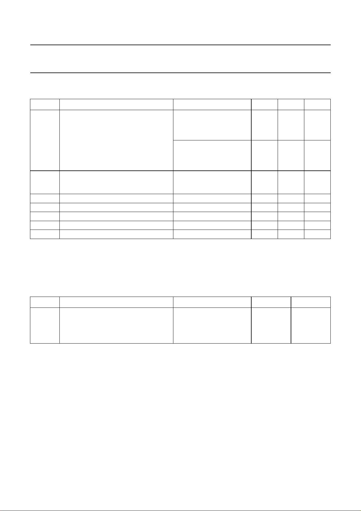
QUICK REFERENCE DATA
SYMBOL PARAMETER CONDITIONS MIN. TYP. MAX. UNIT
V
P
I
P
V
i(VIF)(rms)
V
o(CVBS)(p-p)
B
v(−3dB)
S/N
W
α
IM(1.1)
α
IM(3.3)
α
H(sup)
V
i(SIF)(rms)
V
o(FM)(rms)
V
o(AM)(rms)
THD
audio
S/N
W(audio)
supply voltage 4.5 5 5.5 V
supply current 76 90 104 mA
vision IF input signal voltagesensitivity
−1 dB video at output − 60 100 µV
(RMS value)
video output signal voltage
0.97 1.1 1.23 V
(peak-to-peak value)
−3 dB video bandwidth on pin CVBS B/G and L standard;
78−MHz
CL< 50 pF; RL>1kΩ; AC load
weighted signal-to-noise ratio for video 56 60 − dB
intermodulation attenuation at ‘blue’ f = 1.1 MHz 58 64 − dB
intermodulation attenuation at ‘blue’ f = 3.3 MHz 58 64 − dB
suppression of video signal harmonics 35 40 − dB
sound IF input signal voltage
−3 dB at intercarrier output − 50 100 µV
sensitivity (RMS value)
audio output signal voltage for FM
(RMS value)
B/G standard; 27 kHz,
54% modulation
M/N standard;
0.4 0.5 0.6 V
0.36 0.45 0.54 V
25 kHz modulation
audio output signal voltage for AM
L standard; 54% modulation 0.4 0.5 0.6 V
(RMS value)
total harmonic distortion audio signal 54% modulation
FM − 0.2 0.5 %
AM − 0.5 1.0 %
weighted signal-to-noise ratio audio
54% modulation
signal
FM 55 60 − dB
AM 47 53 − dB
2001 Oct 19 3
Page 4
This text is here in white to force landscape pages to be rotated correctly when browsing through the pdf in the Acrobat reader.This text is here in
_white to force landscape pages to be rotated correctly when browsing through the pdf in the Acrobat reader.This text is here inThis text is here in
white to force landscape pages to be rotated correctly when browsing through the pdf in the Acrobat reader. white to force landscape pages to be ...
2001 Oct 19 4
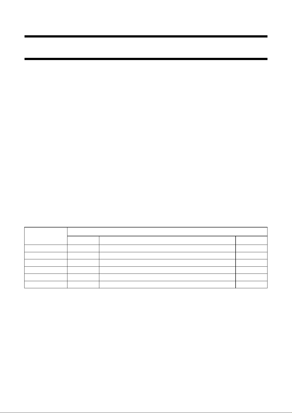
L/L accent switch
and adjust
2 × f
pc
C
VIF
SAW
SIF
SAW
TAGC
VIF1
VIF2
SIF1
SIF2
C
14
TUNER
AGC
1
2
23
24
VIF AMPLIFIER FPLL
SIF AMPLIFIER
VAGC
BLTOP LADJ VCO2 VCO1
(1)
422
VIF
AGC
T
PLL
615
(1)
7
QSS MIXER
INTERCARRIER MIXER
AM DEMODULATOR
VCO
TWD
AFC
DETECTOR
VIDEO
DEMODULATOR
AND AMPLIFIER
AFC
V
P
VOLTAGE
REFERENCE
GND
2021171819
16
8
CVBS
1.1 V (p-p)
AF
SOUND
TRAP
video
1 V (p-p)
audio
BLOCK DIAGRAM
Philips Semiconductors Preliminary specification
Single/multistandard VIF/SIF-PLL and
FM-PLL/AM demodulators
intercarrier
mode
SIF
AGC
(1) Not connected for TDA9817, TDA9817T and TDA9817TS.
INTERCARRIER
MODE SWITCH
5
C
SAGC
standards
selection
switch
(1)
3
TDA9817
TDA9818
Fig.1 Block diagram.
12
QSSSTD
5.5 MHz
handbook, full pagewidth
13
FM
FM-PLL
DEMODULATOR
10 11
9
V
in
de-em
mute
switch
C
de-em
C
DEC
MHA663
TDA9817; TDA9818
Page 5
Philips Semiconductors Preliminary specification
Single/multistandard VIF/SIF-PLL and
FM-PLL/AM demodulators
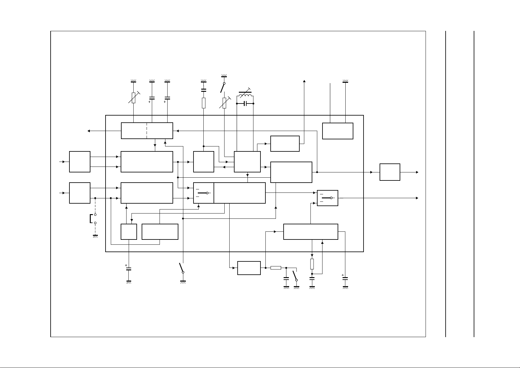
PINNING
SYMBOL PIN DESCRIPTION
VIF1 1 VIF differential input signal voltage 1
VIF2 2 VIF differential input signal voltage 2
STD 3 standards selection switch; note 1
C
VAGC
C
SAGC
T
PLL
LADJ 7 L/L accent switch and adjust; note 1
AF 8 audio output
V
de-em
C
de-em
C
DEC
QSS 12 single reference QSS/intercarrier
FM
in
TAGC 14 tuner AGC output
C
BL
CVBS 16 composite video output voltage
AFC 17 AFC output
VCO1 18 VCO1 resonance circuit
VCO2 19 VCO2 resonance circuit
GND 20 ground
V
P
TOP 22 tuner AGC takeover point adjust
SIF1 23 SIF differential input signal voltage1
SIF2 24 SIF differential input signal voltage2
4 VIF AGC capacitor
5 SIF AGC capacitor
6 PLL filter
9 de-emphasis output
10 de-emphasis input
11 decoupling capacitor
output voltage
13 sound intercarrier input voltage
15 black level detector; note 1
21 supply voltage
handbook, halfpage
C
C
LADJ
V
C
(1) Not connected for TDA9817.
VIF1
VIF2
STD
VAGC
SAGC
T
PLL
de-em
de-em
C
DEC
QSS
AF
1
2
(1)
3
4
5
6
(1)
7
8
9
10
11
12
Fig.2 Pin configuration SDIP24.
TDA9817; TDA9818
SIF2
24
SIF1
23
TOP
22
V
21
P
GND
20
VCO2
MHA664
19
VCO1
18
AFC
17
CVBS
16
(1)
C
15
BL
TAGC
14
13
FM
in
TDA9818
TDA9817
Note
1. Not connected for TDA9817, TDA9817T and
TDA9817TS.
2001 Oct 19 5
Page 6
Philips Semiconductors Preliminary specification
Single/multistandard VIF/SIF-PLL and
FM-PLL/AM demodulators
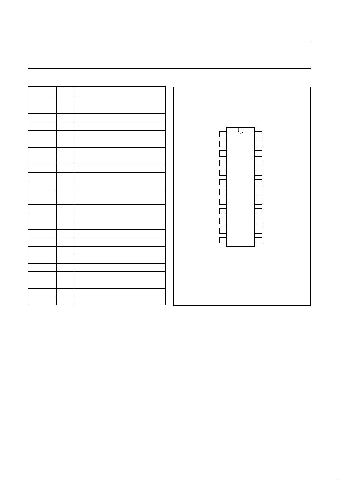
handbook, halfpage
STD
C
VAGC
C
SAGC
T
LADJ
V
de-em
C
de-em
C
VIF1
VIF2
PLL
AF
DEC
QSS
1
2
(1)
3
4
5
6
TDA9818T
7
8
9
10
11
12
TDA9817T
(1)
MGU397
24
SIF2
23
SIF1
22
TOP
21
V
P
GND
20
VCO2
19
VCO1
18
AFC
17
CVBS
16
(1)
15
C
BL
14
TAGC
FM
13
in
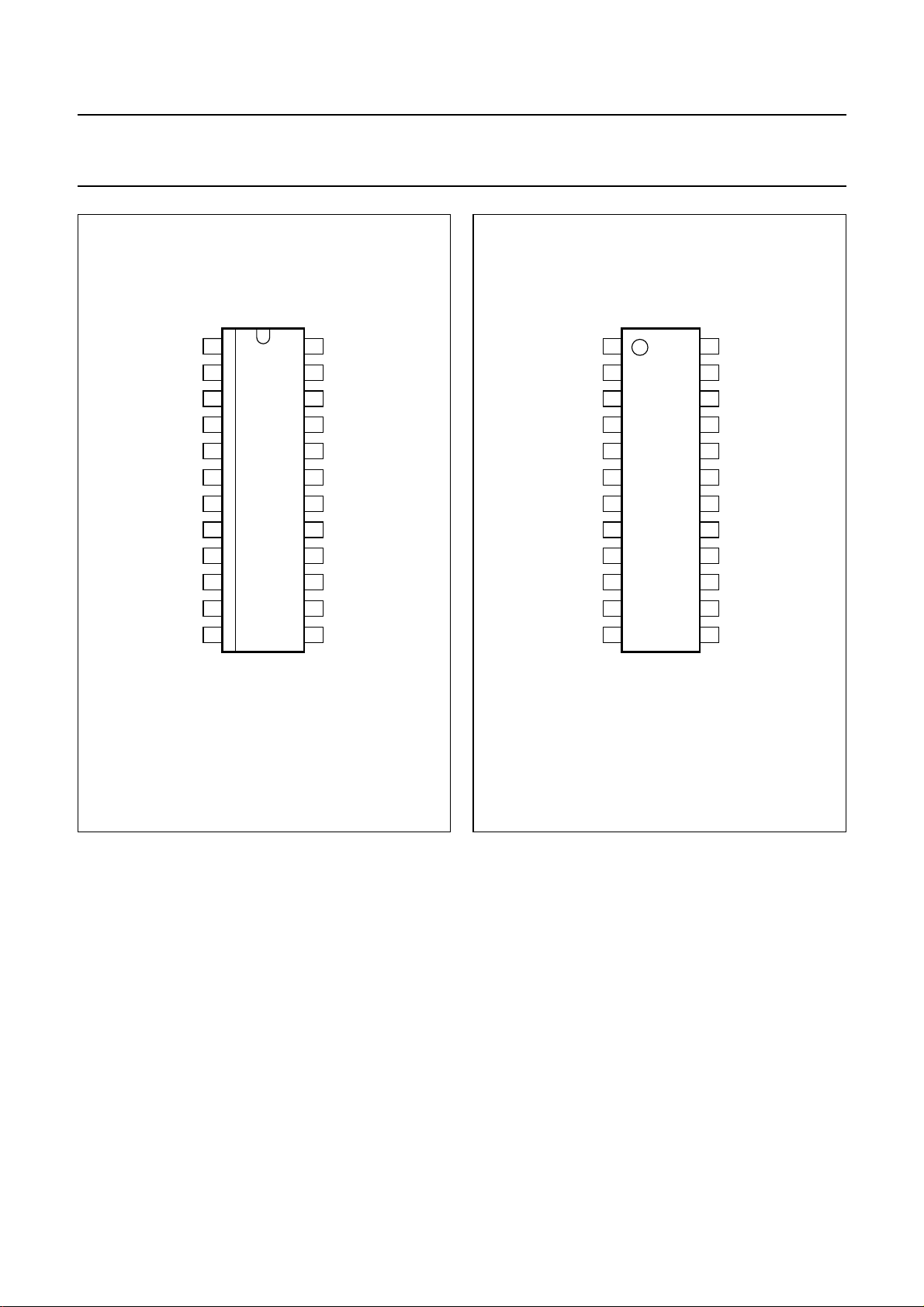
handbook, halfpage
STD
C
VAGC
C
SAGC
T
LADJ
V
de-em
C
de-em
C
VIF1
VIF2
PLL
AF
DEC
QSS
(1)
(1)
10
11
12
TDA9817; TDA9818
1
2
3
4
5
6
TDA9818TS
TDA9817TS
7
8
9
MGU398
24
SIF2
23
SIF1
22
TOP
21
V
P
20
GND
19
VCO2
18
VCO1
17
AFC
CVBS
16
(1)
15
C
BL
14
TAGC
FM
13
in
(1) Not connected for TDA9817T.
Fig.3 Pin configuration SO24.
2001 Oct 19 6
(1) Not connected for TDA9817TS.
Fig.4 Pin configuration SSOP24.
Page 7

Philips Semiconductors Preliminary specification
Single/multistandard VIF/SIF-PLL and
FM-PLL/AM demodulators
FUNCTIONAL DESCRIPTION
The integrated circuit comprises the functional blocks as
shown in Fig.1:
• Vision IF amplifier and VIF AGC detector
• Tuner AGC
• Frequency Phase Locked Loop detector (FPLL)
• VCO, Travelling Wave Divider (TWD) and AFC
• Video demodulator and amplifier
• Sound IF amplifier and SIF AGC
• Single reference QSS mixer
• AM demodulator
• FM-PLL demodulator
• Audio Frequency (AF) signal processing
• Internal voltage stabilizer.
Vision IF amplifier and VIF AGC detector
The vision IF amplifier consists of three AC-coupled
differential amplifier stages. Each differential stage
comprises a feedback network controlled by emitter
degeneration.
The AGC detector generates therequired VIF gain control
voltage for constant video output by charging/discharging
the AGC capacitor. Therefore for negative video
modulation the sync level and for positive video
modulation the peak white level of the video signal is
detected. In order to reduce the reaction time for positive
modulation, where a very large time constant is needed,
an additional level detector increases the discharging
current of the AGC capacitor (fast mode) in the event of a
decreasing VIF amplitude step. The additional level
information is given by the black-level detector voltage.
Tuner AGC
The AGC capacitor voltage is converted to an internal
IF control signal, and is fed to the tuner AGC to generate
the tuner AGC output current at pin TAGC (open-collector
output). The tuner AGC takeover point can be adjusted at
pin TADJ. This allows to match the tuner to the SAW filter
in order to achieve the optimum IF input level.
Frequency Phase Locked Loop detector (FPLL)
The VIF-amplifier output signal is fed into a frequency
detector and into a phase detector via a limiting amplifier.
During acquisition the frequency detector produces a
DC current proportional to the frequency difference
between the input and the VCO signal. After frequency
lock-in the phase detector produces a DC current
TDA9817; TDA9818
proportionalto the phase differencebetween the VCO and
the input signal. The DC current of either frequency
detector or phase detector is converted into a DC voltage
viathe loop filter, whichcontrols the VCO frequency.Inthe
event of positive modulated signals the phase detector is
gated by composite sync in order to avoid signal distortion
for overmodulated VIF signals.
VCO, Travelling Wave Divider (TWD) and AFC
The VCO operates with a resonance circuit (with L and C
in parallel) at double the picture carrier frequency. The
VCO is controlled by two integrated variable capacitors.
The control voltage required to tune the VCO from its
free-running frequency to actually double the picture
carrier frequency is generated by the frequency-phase
detector (FPLL) and fed via the loop filter to the first
variable capacitor. This control voltage is amplified and
additionally converted into a current which represents the
AFC output signal. At centre frequency the AFC output
current is equal to zero.
For TDA9818: the VCO centre frequency can be
decreased (required for L accent standard) by activating
an additional internal capacitor. This is achieved by using
the L accent switch. In this event the second variable
capacitor can be controlled by a variable resistor at the
L accentswitchforsettingtheVCOcentrefrequencytothe
required L accent value.
The oscillator signal is divided by 2 with a TWD which
generates two differential output signals with a 90 degree
phase difference independent of the frequency.
Video demodulator and amplifier
The video demodulator is realized by a multiplier which is
designed for low distortion and large bandwidth. The
vision IF input signal is multiplied with the ‘in phase’ signal
of the travelling wave divider output. In the demodulator
stage the video signal polarity can be switched in
accordance with the TV standard.
The demodulator output signal is fed via an integrated
low-pass filter for attenuation of the carrier harmonics to
the video amplifier. The video amplifier is realized by an
operational amplifier with internal feedback and high
bandwidth. A low-pass filter is integrated to achieve an
attenuation of the carrier harmonics for B/G and
L standard. The standard dependent level shift in this
stage delivers the same sync level for positive and
negative modulation. The video output signal at pin CVBS
is 1.1 V (p-p) for nominal vision IF modulation, in order to
achieve 1 V (p-p) at sound trap output.
2001 Oct 19 7
Page 8

Philips Semiconductors Preliminary specification
Single/multistandard VIF/SIF-PLL and
FM-PLL/AM demodulators
Sound IF amplifier and SIF AGC
The sound IF amplifier consists of two AC-coupled
differential amplifier stages. Each differential stage
comprises a controlled feedback network provided by
emitter degeneration.
The SIF AGC detector is related to the SIF input signal
(average level of AM or FM carrier) and controls the SIF
amplifier to provide a constant SIF signal to the
AM demodulator and single reference QSS mixer. At
L standard (AM sound) the SIF AGC reaction time is set to
‘slow’ for nominal video conditions. But with a decreasing
VIF amplitude step the SIF AGC is set to ‘fast’ mode
controlled by the VIF AGC detector. In FM mode this
reaction time is always ‘fast’.
Single reference QSS mixer
The single reference QSS mixeris realized by a multiplier.
The SIF amplifier output signal is fed to the single
reference QSS mixer and converted to intercarrier
frequency by the regenerated picture carrier (VCO). The
mixer output signal is fed via a high-pass for attenuation of
the video signal components to the output pin QSS. With
this system a high performance hi-fi stereo sound
processing can be achieved.
For a simplified application without a sound IF SAW filter
the single reference QSS mixer can be switched to the
intercarrier mode byconnecting pin SIF2 to ground. In this
mode the sound IF passes the vision IF SAW filter and the
composite IF signal is fed to the single reference QSS
mixer. This IF signal is multiplied with the 90 degree TWD
output signal for converting the sound IF to intercarrier
frequency. This composite intercarrier signal is fed to the
output pin QSS, too. By using this quadrature detection,
the low frequency video signals are removed.
AM demodulator
The AM demodulator is realized by a multiplier. The
modulated SIF amplifier output signal is multiplied in
phase with the limited (AM is removed) SIF amplifier
output signal. The demodulator output signal is fed via an
integrated low-pass filter for attenuation of the carrier
harmonics to the AF amplifier.
TDA9817; TDA9818
FM-PLL demodulator
The FM-PLL demodulator consists of a limiter and an
FM-PLL. The limiter provides the amplification and
limitation of the FM sound intercarrier signal. The result is
high sensitivity and AM suppression. The amplifier
consists of 7 stages which are internally AC-coupled in
order to minimize the DC offset.
Furthermore the AF output signal can be muted by
connecting a resistor between the limiter input pin FM
and ground.
TheFM-PLL consists of anintegrated relaxation oscillator,
an integrated loop filter and a phase detector. The
oscillator is locked to the FM intercarrier signal, output
from the limiter. As a result of locking, the oscillator
frequency tracks with the modulation of the input signal
and the oscillator control voltage is superimposed by the
AF voltage. The FM-PLL operates as an FM demodulator.
Audio Frequency signal processing
The AF amplifier consists of two parts:
1. The AF pre-amplifier for FM sound is an operational
amplifier with internal feedback, high gain and high
common mode rejection. The AF voltage from the
PLL demodulator, by principle a small output signal, is
amplified by approximately 33 dB. The low-pass
characteristicoftheamplifierreducestheharmonicsof
the intercarrier signal at the sound output terminal
pin V
sound is applied. An additional DC control circuit is
implemented to keep the DC level constant,
independent of process spread.
2. The AF output amplifier (10 dB) provides the required
output level by a rail-to-rail outputstage. This amplifier
makes use of an input selector for switching to AM,
FM de-emphasis or mute state, controlled by the
standard switching voltage and the mute switching
voltage.
Internal voltage stabilizer
The bandgap circuit internally generates a voltage of
approximately 1.25 V, independent of supply voltage and
temperature. A voltage regulator circuit, connected to this
voltage, produces a constant voltage of 3.6 V which is
used as an internal reference voltage.
at which the de-emphasis network for FM
de-em
in
2001 Oct 19 8
Page 9
Philips Semiconductors Preliminary specification
Single/multistandard VIF/SIF-PLL and
TDA9817; TDA9818
FM-PLL/AM demodulators
LIMITING VALUES
In accordance with the Absolute Maximum Rating System (IEC 60134).
SYMBOL PARAMETER CONDITIONS MIN. MAX. UNIT
V
P
V
n
t
sc(max)
V
TAGC
T
stg
T
amb
V
esd
supply voltage TDA9817, TDA9817T,
TDA9818 and TDA9818T:
maximum chip temperature
of 120 °C; note 1
TDA9817TS and
TDA9818TS: maximum chip
temperature of 130 °C;
note 1
voltage at pins VIF1, VIF2, STD, C
C
, T
SAGC
PLL
, V
de-em
, C
de-em
, C
DEC
VAGC
, FMin,
,
TAGC, CBL, AFC, VP, TOP, SIF1 and SIF2
maximum short-circuit time to ground or V
P
tuner automatic gain control output voltage 0 13.2 V
storage temperature −25 +150 °C
ambient temperature −20 +70 °C
electrostatic handling voltage note 2 −300 +300 V
− 5.5 V
− 5.5 V
0V
P
− 10 s
V
Notes
1. I
= 104 mA; T
P
TDA9818T, R
=70°C; R
amb
= 110 K/W for TDA9817TS and TDA9818TS.
th(j-a)
= 65 K/W for TDA9817 and TDA9818, R
th(j-a)
= 85 K/W for TDA9817T and
th(j-a)
2. Machine model class B (L = 2.5 µH).
THERMAL CHARACTERISTICS
SYMBOL PARAMETER CONDITIONS VALUE UNIT
R
th(j-a)
thermal resistance from junction to ambient in free air
TDA9817; TDA9818 65 K/W
TDA9817T; TDA9818T 85 K/W
TDA9817TS; TDA9818TS 110 K/W
2001 Oct 19 9
Page 10
Philips Semiconductors Preliminary specification
Single/multistandard VIF/SIF-PLL and
TDA9817; TDA9818
FM-PLL/AM demodulators
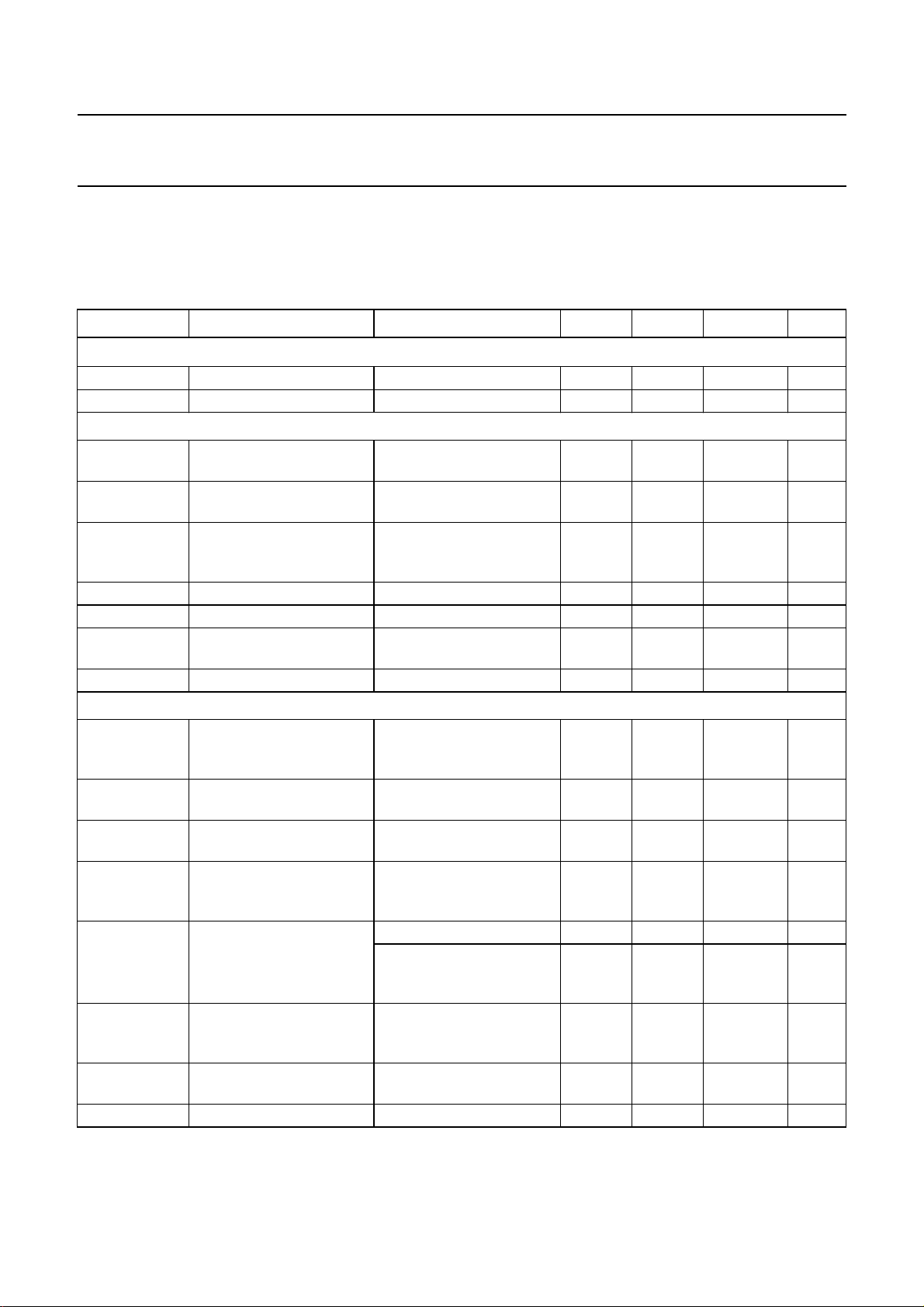
CHARACTERISTICS
VP=5V; T
peak white level for L); IF input from 50 Ω via broadband transformer 1 : 1; video modulation DSB; residual carrier
B/G: 10%; L = 3%; video signal in accordance with
Fig.15; unless otherwise specified.
SYMBOL PARAMETER CONDITIONS MIN. TYP. MAX. UNIT
Supply (pin V
V
P
I
P
Vision IF amplifier (pins VIF1 and VIF2)
V
i(VIF)(rms)
V
i(VIF)(max)(rms)
∆V
(IF)(int)
G
IF(ctrl)
R
i(dif)
C
i(dif)
V
I(VIF)
True synchronous video demodulator; note 3
f
VCO(max)
∆f
/∆T oscillator drift as a function
osc
∆f
/∆V
osc
V
VCO(rms)
f
cr(pc)
∆f
pc(fr)
f
algn(Laccent)
t
acq
=25°C; see Table 1 for input frequencies and levels; input level V
amb
“CCIR, line 17”
)
P
or
supply voltage note 1 4.5 5 5.5 V
supply current 76 90 104 mA
input signal voltage
sensitivity (RMS value)
maximum input signal
voltage (RMS value)
internal IF amplitude
difference between picture
and sound carrier
B/G standard; −1 dB video
at output
B/G standard; 1 dB video
at output
within AGC range;
B/G standard;
∆f = 5.5 MHz
IF gain control range see Fig.5 65 70 − dB
differential input resistance note 2 1.7 2.2 2.7 kΩ
differential input
note 2 1.2 1.7 2.5 pF
capacitance
DC input voltage note 2 − 3.4 − V
maximum oscillator
f=2f
pc
frequency for carrier
regeneration
oscillator is free-running;
of temperature
P
oscillator shift as a
function of supply voltage
I
= 0; note 4
AFC
oscillator is free-running;
note 4
oscillator voltage swing at
pins VCO1 and VCO2
(RMS value)
picture carrier capture
range
picture carrier frequency
(free-running) accuracy
L accent alignment
B/G, M/N and L standard ±1.4 ±1.8 − MHz
L accent standard;
f
= 33.9 MHz;
pc
R
= 5.6 kΩ
LADJ
L accent standard;
fpc= 33.9 MHz;
R
= 5.6 kΩ
LADJ
L accent standard; I
AFC
frequency range
acquisition time BL = 70 kHz; note 5 −−30 ms
i(VIF)(rms)
“NTC-7 Composite”
= 10 mV (sync level for B/G,
; measurements taken in
− 60 100 µV
120 200 − mV
− 0.7 1 dB
125 130 − MHz
−−±20 × 10−6K
−−±1.5 × 10⁻³V
50 80 110 mV
±0.9 ±1.2 − MHz
−±200 ±400 kHz
=0 ±400 ±600 − kHz
−1
−1
2001 Oct 19 10
Page 11

Philips Semiconductors Preliminary specification
Single/multistandard VIF/SIF-PLL and
TDA9817; TDA9818
FM-PLL/AM demodulators
SYMBOL PARAMETER CONDITIONS MIN. TYP. MAX. UNIT
V
i(VIF)(sens)(rms)
Composite video amplifier (pin CVBS); sound carrier off
V
o(CVBS)(p-p)
V/S ratio between video
∆V
o(CVBS)
V
sync
V
clip(u)
V
clip(l)
R
o
I
bias(int)
I
o(sink)(max)
I
o(source)(max)
∆V
o(CVBS)(B/G)
∆V
o(BL)(B/G)
∆V
o(BL)(L)
G
dif
ϕ
dif
B
v(−1dB)
B
v(−3dB)
S/N
W
S/N unweightedsignal-to-noise
VIF input signal voltage
maximum IF gain; note 6 − 30 70 µV
sensitivity for PLL to be
locked (RMS value);
pins VIF1 and VIF2
output signal voltage
see Fig.10 0.97 1.1 1.23 V
(peak-to-peak value)
1.9 2.33 3.0
(black-to-white) and sync
level
output signal voltage
difference
difference between B/G
and L standard
−−±12 %
sync voltage level B/G and L standard 1.4 1.5 1.6 V
upper video clipping
VP− 1.1 VP− 1 − V
voltage level
lower video clipping
− 0.7 0.9 V
voltage level
output resistance note 2 −−10 Ω
internal DC bias current for
2.2 3.0 − mA
emitter-follower
maximum AC and DC
1.6 −− mA
output sink current
maximum AC and DC
2.9 −− mA
output source current
deviation of CVBS output
signal voltage at
50 dB gain control −−0.5 dB
30 dB gain control −−0.1 dB
B/G standard
black level tilt in
gain variation; note 7 −−1%
B/G standard
vertical black level tilt for
worst case in L standard
vision carrier modulated by
test line (VITS) only; gain
−−1.9 %
variation; note 7
differential gain
differential phase
−1 dB video bandwidth B/G and L standard;
“CCIR, line 330”
“CCIR, line 330”
− 25 %
− 1 2 deg
56− MHz
CL< 50 pF; RL> 1kΩ;
AC load
−3 dB video bandwidth B/G and L standard;
78− MHz
CL< 50 pF; RL> 1kΩ;
AC load
weighted signal-to-noise
see Fig.7; note 8 56 60 − dB
ratio
see Fig.7; note 8 49 53 − dB
ratio
2001 Oct 19 11
Page 12

Philips Semiconductors Preliminary specification
Single/multistandard VIF/SIF-PLL and
TDA9817; TDA9818
FM-PLL/AM demodulators
SYMBOL PARAMETER CONDITIONS MIN. TYP. MAX. UNIT
α
IM(1.1)
α
IM(3.3)
∆f
unwanted(p-p)
∆ϕ robustness for modulator
α
vc(rms)
α
H(sup)
α
H(spur)
PSRR power supply ripple
VIF AGC detector (pins C
I
ch
I
dch
t
resp(inc)
t
resp(dec)
∆IF VIF amplitude step for
V
th(CBL)
intermodulation
attenuation at ‘blue’
intermodulation
attenuation at ‘yellow’
intermodulation
attenuation at ‘blue’
intermodulation
attenuation at ‘yellow’
robustness for unwanted
frequency deviation of
picture carrier
(peak-to-peak value)
imbalance
f = 1.1 MHz; see Fig.8;
note 9
f = 1.1 MHz; see Fig.8;
note 9
f = 3.3 MHz; see Fig.8;
note 9
f = 3.3 MHz; see Fig.8;
note 9
L standard;
residual carrier: 3%;
serration pulses: 50%;
note 2
L standard;
residual carrier: 0%;
58 64 − dB
60 66 − dB
58 64 − dB
59 65 − dB
−−12 kHz
−−3%
serration pulses: 50%;
note 2
residual vision carrier
(RMS value)
fundamental wave and
harmonics; B/G and
− 25 mV
L standard
suppression of video
note 10a 35 40 − dB
signal harmonics
spurious elements note 10b 40 −− dB
video signal; grey level;
rejection at pin CVBS
see Fig.13
B/G standard 30 35 − dB
L standard 26 30 − dB
and CBL)
VAGC
charging current B/G and L standard; note 7 0.75 1 1.25 mA
additional charging current L standard in event of
1.9 2.5 3.1 µA
missing VITS pulses and
no white video content
discharging current B/G standard 15 20 25 µA
normal mode L 225 300 375 nA
fast mode L 30 40 50 µA
AGC response to an
increasing VIF step
AGC response to a
decreasing VIF step
B/G and L standard;
− 0.05 0.1 ms/dB
note 11
B/G standard − 2.2 3.5 ms/dB
fast mode L − 1.1 1.8 ms/dB
normal mode L; note 11 − 150 240 ms/dB
L standard −2 −6 −10 dB
activating fast AGC mode
threshold voltage level
additional charging current
see Fig.10
L standard 1.95 2.0 2.05 V
L standard; fast mode L 1.6 1.66 1.72 V
2001 Oct 19 12
Page 13

Philips Semiconductors Preliminary specification
Single/multistandard VIF/SIF-PLL and
TDA9817; TDA9818
FM-PLL/AM demodulators
SYMBOL PARAMETER CONDITIONS MIN. TYP. MAX. UNIT
Tuner AGC (pin TAGC)
V
i(rms)
IF input signal voltage for
minimum starting point of
tuner takeover
(RMS value)
IF input signal voltage for
maximum starting point of
tuner takeover
(RMS value)
V
o(TAGC)
V
sat(TAGC)
∆V
TOP(TAGC)
permissible output voltage from external source;
saturation voltage I
/∆T variation of takeover point
by temperature
I
TAGC(sink)
∆G
IF
sink current see Fig.5
IF slip by automatic gain
control
AFC circuit (pin AFC); see Fig.9; note 12
CR
stps
∆f
/∆T frequency variation by
IF
control steepness ∆I
AFC
temperature
V
o(AFC)
I
o(source)(AFC)
I
o(sink)(AFC)
∆I
AFC(p-p)
output voltage upper limit VP− 0.6 VP− 0.3 − V
output source current 150 200 250 µA
output sink current 150 200 250 µA
residual video modulation
current
(peak-to-peak value)
input at pins VIF1
and VIF2; R
I
TAGC
TOP
= 0.4 mA
input at pins VIF1
and VIF2; R
I
TAGC
TOP
= 0.4 mA
=22kΩ;
=0Ω;
− 25 mV
50 100 − mV
−−13.2 V
note 2
= 1.5 mA −−0.2 V
TAGC
I
= 0.4 mA − 0.03 0.07 dB/K
TAGC
no tuner gain reduction;
V
= 13.2 V
TAGC
maximum tuner gain
−−5 µA
1.5 2 2.6 mA
reduction
tuner gain current from
− 68 dB
20% to 80%
/∆f note 13
33.9 MHz 0.5 0.75 1.0 µA/kHz
38.9 MHz 0.5 0.75 1.0 µA/kHz
45.75 MHz 0.45 0.65 0.85 µA/kHz
58.75 MHz 0.38 0.55 0.72 µA/kHz
B/G and L standard;
I
= 0; note 4
AFC
L accent standard;
I
= 0; note 4
AFC
−−±20 × 10−6K
−−±60 × 10−6K
lower limit − 0.3 0.6 V
B/G and L standard − 20 30 µA
−1
−1
2001 Oct 19 13
Page 14

Philips Semiconductors Preliminary specification
Single/multistandard VIF/SIF-PLL and
TDA9817; TDA9818
FM-PLL/AM demodulators
SYMBOL PARAMETER CONDITIONS MIN. TYP. MAX. UNIT
Sound IF amplifier (pins SIF1 and SIF2)
V
i(SIF)(rms)
input signal voltage
sensitivity (RMS value)
V
i(max)(rms)
maximum input signal
voltage (RMS value)
G
SIF(ctrl)
R
i(dif)
C
i(dif)
SIF gain control range FM and AM mode;
differential input resistance note 2 1.7 2.2 2.7 kΩ
differential input
capacitance
V
I(SIF)
α
SIF,VIF
DC input voltage − 3.4 − V
crosstalk attenuation
between SIF and VIF
inputs
SIF AGC detector (pin C
I
ch(CSAGC)
I
dch(CSAGC)
charging current FM mode 8 12 16 µA
discharging current FM mode 8 12 16 µA
SAGC
)
Single reference QSS intercarrier mixer (B/G standard; pin QSS)
V
o(rms)
IF intercarrier output level
(RMS value)
V
o(peak)
IF intercarrier output level
(peak value)
B
s(−3dB)
−3 dB intercarrier
bandwidth
α
sc(rms)
residual sound carrier
(RMS value)
FM mode; −3 dB at
− 50 100 µV
intercarrier output pin QSS
AM mode; −3 dB at
− 50 100 µV
AF output pin AF
FM mode; 1 dB at
65 100 − mV
intercarrier output pin QSS
AM mode; 1 dB at
65 100 − mV
AF output pin AF
60 66 − dB
see Fig.6
note 2 1.2 1.7 2.5 pF
between pins VIF1
50 −− dB
and VIF2, and pins SIF1
and SIF2; note 14
AM mode 0.8 1.2 1.6 µA
normal mode AM 1 1.4 1.8 µA
fast mode AM 60 85 110 µA
QSS mode;
100 140 180 mV
sound carrier 1;
sound carrier 2 off
L standard; without
100 140 180 mV
modulation
intercarrier mode;
− note 15 − mV
sound carrier 1;
sound carrier 2 off
QSS mode 141 198 225 mV
L standard;
255 356 458 mV
80% AM modulation
upper limit 7.5 9 − MHz
QSS mode; fundamental
− 25 mV
wave and harmonics
intercarrier mode;
− 25 mV
fundamental wave and
harmonics
2001 Oct 19 14
Page 15

Philips Semiconductors Preliminary specification
Single/multistandard VIF/SIF-PLL and
TDA9817; TDA9818
FM-PLL/AM demodulators
SYMBOL PARAMETER CONDITIONS MIN. TYP. MAX. UNIT
α
vc(rms)
α
H(sup)
R
o(QSS)
V
O(QSS)
I
int(QSS)
I
sink(max)(QSS)
I
source(max)(QSS)
Limiter amplifier (pin FMin); note 16
residual vision carrier
(RMS value)
QSS mode; fundamental
wave and harmonics
intercarrier mode;
− 25 mV
− 520 mV
fundamental wave and
harmonics
suppression of video
signal harmonics
intercarrier mode;
f
≤ 5 MHz
video
39 −− dB
output resistance note 2 −−25 Ω
DC output voltage − 2.0 − V
DC internal bias current for
1.9 2.5 − mA
emitter follower
maximum AC and DC
1.4 1.9 − mA
output sink current
maximum AC and DC
3.0 3.5 − mA
output source current
V
i(FMin)(rms)
input signal voltage for
lock-in (RMS value)
V
i(FMin)(rms)
input signal voltage
(RMS value)
allowed input signal
voltage (RMS value)
α
AM
R
i(FMin)
V
I(FMin)
AM suppression 50 µs de-emphasis;
input resistance note 2 480 600 720 Ω
DC input voltage − 2.8 − V
FM-PLL demodulator
f
f
t
cr
hr
acq
catching range of PLL upper limit 7.0 −− MHz
holding range of PLL upper limit 9.0 −− MHz
acquisition time −−4 µs
−−100 µV
SN+
-------------N
weighted
− 250 400 µV
40 dB=
200 −− mV
46 50 − dB
AM: f = 1 kHz; m = 0.3
refer to 27 kHz
(54% FM deviation)
lower limit −−4.0 MHz
lower limit −−3.5 MHz
2001 Oct 19 15
Page 16

Philips Semiconductors Preliminary specification
Single/multistandard VIF/SIF-PLL and
TDA9817; TDA9818
FM-PLL/AM demodulators
SYMBOL PARAMETER CONDITIONS MIN. TYP. MAX. UNIT
FM operation (B/G standard; pin AF); notes 16 and 16a
V
o(AF)(rms)
AF output signal voltage
(RMS value)
V
o(AF)(clip)
AF output clipping signal
voltage level
∆f
AF
∆V
/∆T temperature drift of
o
frequency deviation THD < 1.5%; note 17 −−±53 kHz
AF output signal voltage
V
de-em(DC)
DC voltage at decoupling
capacitor
R
AF
V
AF
I
sink(max)(AF)
output resistance note 2 −−100 Ω
DC output voltage − 2.3 − V
maximum AC and DC
output sink current
I
source(max)(AF)
maximum AC and DC
output source current
B
AF(−3dB)
−3 dB audio frequency
bandwidth
THD total harmonic distortion 27 kHz
S/N
W
weighted signal-to-noise
ratio
α
sc(rms)
residual sound carrier
(RMS value)
α
AF
mute attenuation of
AF signal
∆V
AF
DC jump voltage of
AF output terminal for
switching AF output to
mute state and vice versa
PSRR power supply ripple
rejection at pin AF
27 kHz
(54% FM deviation);
see Fig.15; note 17
R
= 470 Ω 200 250 300 mV
x
R
=0Ω 400 500 600 mV
x
25 kHz
360 450 540 mV
(50% FM deviation);
=0Ω; see Fig.15;
R
x
note 17
THD < 1.5% 1.0 − 1.2 V
−3
voltagedependentonVCO
− 3 × 10−37 × 10
1.2 − 3.0 V
frequency; note 18
−−0.5 mA
−−0.5 mA
without de-emphasis
100 125 − kHz
capacitor
− 0.2 0.5 %
(54% FM deviation)
FM-PLL only; with 50 µs
55 60 − dB
de-emphasis; 27 kHz
(54% FM deviation);
“CCIR 468-4”
fundamental wave and
−−75 mV
harmonics
B/G and L standard 70 75 − dB
FM-PLL in lock mode −±50 ±150 mV
=0Ω; f = 70 Hz;
R
x
20 26 − dB
see Figs 13 and 15
dB/K
2001 Oct 19 16
Page 17

Philips Semiconductors Preliminary specification
Single/multistandard VIF/SIF-PLL and
TDA9817; TDA9818
FM-PLL/AM demodulators
SYMBOL PARAMETER CONDITIONS MIN. TYP. MAX. UNIT
Single reference QSS AF performance for FM operation (B/G standard); see Table 1; notes 19, 20 and 21
S/N
W
weighted signal-to-noise
ratio
Intercarrier AF performance for FM operation (standard B/G); see Table 1; notes 19, 20 and 22
S/N
W
weighted signal-to-noise
ratio
AM operation (L standard; pin AF); note 23
V
o(AF)(rms)
AF output signal voltage
(RMS value)
THD total harmonic distortion 54% modulation − 0.5 1.0 %
B
AF(−3dB)
S/N
W
−3 dB AF bandwidth 100 125 − kHz
weighted signal-to-noise
ratio
V
AF
DC potential voltage − 2.3 − V
PSRR power supply ripple
rejection at pin AF
Switching level for standard switch (pin STD)
V
logic
DC potential for logic
HIGH or pin not connected
DC potential for logic LOW L/L accent standard 0 − 0.8 V
I
IL
LOW level input current Vi= 0 V 190 250 310 µA
pc/sc1 ratio at pins VIF1
40 −− dB
and VIF2; 27 kHz
(54% FM deviation);
“CCIR 468-4”
black picture 53 58 − dB
white picture 50 55 − dB
6 kHz sine wave
42 48 − dB
(black-to-white
modulation)
sound carrier
45 51 − dB
subharmonics;
f = 2.75 MHz ±3 kHz
pc/sc1 ratio at pins VIF1
27 −− dB
andVIF2;27 kHz(54% FM
deviation);
“CCIR 468-4”
black picture 47 51 − dB
white picture 47 51 − dB
6 kHz sine wave
40 46 − dB
(black-to-white
modulation)
sound carrier
35 39 − dB
subharmonics;
f = 2.75 MHz ±3 kHz
54% modulation 400 500 600 mV
“CCIR 468-4”
47 53 − dB
see Fig.13 20 26 − dB
B/G standard 2.8 − V
P
V
2001 Oct 19 17
Page 18

Philips Semiconductors Preliminary specification
Single/multistandard VIF/SIF-PLL and
TDA9817; TDA9818
FM-PLL/AM demodulators
Notes
1. Values of video and sound parameters are decreased at VP= 4.5 V.
2. This parameter is not tested during production and is only given as an application information for designing the
television receiver.
3. Loop bandwidth BL = 70 kHz (natural frequency fn= 12 kHz; damping factor d ≈ 3; calculated with sync level within
gain control range). Resonance circuit of VCO: Q0> 50; C
approximately 2.7 V).
4. Temperature coefficient of external LC circuit is equal to zero.
5. V
i(VIF)(rms)
= 10 mV; ∆f = 1 MHz (VCO frequency offset related to picture carrier frequency); white picture
video modulation.
6. VIF signal for nominal video signal.
7. The leakage current of the AGC capacitor should not exceed 1 µA at B/G standard, respectively 10 nA current at
L standard. Larger currents will increase the tilt.
8. S/N is the ratio of black-to-white amplitude to the black level noise voltage (RMS value, pin CVBS). B=5MHz
weighted in accordance with
“CCIR 567”
.
9. The intermodulation figures are defined:
at 4.4 MHz
V
o
α
1.1
α
3.3
20
20
--------------------------------------
at 1.1 MHz
V
o
V
at 4.4 MHz
o
log=
--------------------------------------
at 3.3 MHz
V
o
3.6 dB+log=
; α
; α
value at 1.1 MHz referenced to black/white signal;
1.1
value at 3.3 MHz referenced to colour carrier.
3.3
10. Measurements taken with SAW filter K3953 (sound carrier suppression: 40 dB); loop bandwidth BL = 70 kHz:
a) Modulation VSB; sound carrier off; f
b) Sound carrier on; SIF SAW filter K9453; f
video
> 0.5 MHz.
= 10 kHz to 10 MHz.
video
11. Response speed valid for a VIF input level range of 200 µVupto70mV.
12. To match the AFC output signal to different tuning systems a current source output is provided. The test circuit is
given in Fig.9. The AFC-steepness can be changed by the resistors at pin AFC.
13. Depending on the ratio ∆C/C0 of the LC resonant circuit of VCO (Q0> 50; note 3; C0=C
14. Source impedance: 2.3 kΩ in parallel to 12 pF (SAW filter); fIF= 38.9 MHz.
15. Without using an SIF SAW filter the mixer can be switched to intercarrier mode by connecting pin SIF1 and/or
pin SIF2 to ground. In this mode the SIF passes the VIF SAW filter and IF intercarrier levels are depending on the
sound shelf of the VIF SAW filter. The intercarrier output signal at pin QSS can becalculated by thefollowing formula
taking into account the video output signal at pin CVBS (V
V
i(sc)
dB()6dB 3dB±+
-----------V
i(pc)
V
o(rms)
1.1 V p p–()
× 10
---------- 22
1
------------------------------------------------------------- -
×=
20
= 8.2 pF ±0.25 pF; C
ext
o(CVBS)(p-p)
= 1.1 V typical) as a reference:
where:
≈ 8.5 pF (loop voltage
int
int+Cext
).
1
a) = correction term for RMS value
---------- 22
V
i(sc)
b) = sound-to-picture carrier ratio at VIF inputs in dB
------------- V
i(pc)
(dB)
c) 6 dB = correction term of internal circuitry
d) ±3 dB = tolerance of video output and intercarrier output amplitude V
2001 Oct 19 18
o(rms)
Page 19

Philips Semiconductors Preliminary specification
Single/multistandard VIF/SIF-PLL and
TDA9817; TDA9818
FM-PLL/AM demodulators
e) Example for SAW filter G1962: sound shelf value = 20 dB,
V
i(sc)
------------V
i(pc)
16. Input level for second IF from an external generator with 50 Ω source impedance. AC-coupled with 10 nF capacitor,
f
= 1 kHz, 27 kHz (54% FM deviation) of audio references. A VIF/SIF input signal is not permitted. Pins C
mod
and C
SAGC
taken at 50 µs de-emphasis at pin V
steepness ∆V
a) Second IF input level 10 mV (RMS value).
17. Measured with an FM deviation of 27 kHz the typical AF output signal is 500 mV (RMS) (Rx=0Ω). By using
Rx= 470 Ω the AF output signal is attenuated by 6 dB [250 mV (RMS)]. For handling a frequency deviation of more
than 53 kHz the AF output signal has to be reduced by using Rx in order to avoid clipping (THD < 1.5%). For an
FM deviation up to 100 kHz an attenuation of 6 dB is recommended with Rx= 470 Ω.
18. The leakage current of the decoupling capacitor (2.2 µF) should not exceed 1 µA.
19. For all S/N measurements the used vision IF modulator has to meet the following specifications:
a) Incidental phase modulation for black-to-white jump less than 0.5 degrees
b) QSS AF performance, measured with the television demodulator AMF2 (audio output, weighted S/N ratio) better
than 60 dB (deviation 27 kHz) for 6 kHz sine wave black-to-white video modulation
c) Picture-to-sound carrier ratio; pc/sc1 = 13 dB (transmitter).
20. The pc/sc1 ratio is calculated as the addition of TV transmitter pc/sc1 ratio and SAW filter pc/sc1 ratio. This pc/sc1
ratio is necessary to achieve the S/NW values as noted. A different pc/sc1 ratio will change these values.
21. Measurements taken with SAW filter K3953 for vision IF (suppressed sound carrier) and K9453 for sound IF
(suppressed picture carrier). Input level V
22. Measurements taken with SAW filter G1962 (sound shelf: 20 dB) for vision and sound IF. Pin SIF1 and/or pin SIF2
has to be connected to ground for switching the single reference QSS mixer to intercarrier mode.
23. Measurements taken with SAW filter K9453 (Siemens) for AM sound IF (suppressed picture carrier).
27 dB– V
o(rms)
32 mV (typical value)=⇒=
VAGC
have to be connected to positive supply voltage for minimum IF gain. S/N and THD measurements are
(modulator pre-emphasis has to be activated). The FM demodulator
de-em
/∆fAF is positive.
o(AF)
i(SIF)(rms)
= 10 mV, 27 kHz (54% FM deviation).
Table 1 Input frequencies and carrier ratios
DESCRIPTION SYMBOL B/G STANDARD M/N STANDARD L STANDARD
picture or IF carrier f
sound carrier f
pc
or f
sc1
f
sc2
IF
38.9 45.75/58.75 38.9 33.9 MHz
33.4 41.25/54.25 32.4 40.4 MHz
33.158 −−−MHz
L ACCENT
STANDARD
picture-to-sound carrier sc1 13 7 10 10 dB
sc2 20 −−−dB
2001 Oct 19 19
UNIT
Page 20

Philips Semiconductors Preliminary specification
Single/multistandard VIF/SIF-PLL and
FM-PLL/AM demodulators
; R
70
gain
(dB)
600.06
50
40
30
206
10
060
−10
1 2.521.5 3 3.5 4
TOP
=22kΩ.
(3) I
(4) I
tuner
tuner
; R
; R
TOP
TOP
=11kΩ.
=0Ω.
handbook, full pagewidth
V
i(VIF)(rms)
(mV)
0.6
(1) I
tuner
(2) Gain.
TDA9817; TDA9818
(1) (2) (3) (4)
V
CVAGC
MHA665
(V)
4.5
I
tuner
(mA)
0
1
2
handbook, full pagewidth
V
100
i(SIF)(rms)
(mV)
10
1
0.1
0.01
(dBµV)
Fig.5 Typical VIF and tuner AGC characteristics.
110
100
90
80
70
60
50
40
30
20
1 2.521.5 3 3.5 4
V
CSAGC
MHA666
(V)
4.5
Fig.6 Typical SIF AGC characteristic (FM and AM mode).
2001 Oct 19 20
Page 21

Philips Semiconductors Preliminary specification
Single/multistandard VIF/SIF-PLL and
FM-PLL/AM demodulators
75
handbook, halfpage
S/N
(dB)
50
25
0
−60 −40 −20 20
0.06 0.6 6 60060
TDA9817; TDA9818
MED684
0
V
i(VIF)(rms)
10
V
i(VIF)(rms)
(dB)
(mV)
Fig.7 Typical signal-to-noise ratio as a function of IF input voltage.
handbook, halfpage
13.2 dB
27 dB
sc cc pc sc cc pc
sc = sound carrier, with respect to sync level.
cc = chrominance carrier, with respect to sync level.
pc = picture carrier, with respect to sync level.
The sound carrier levels are taking into account a sound shelf attenuation of 20 dB (SAW filter G1962).
3.2 dB
13.2 dB
27 dB
BLUE YELLOW
10 dB
MED685
Fig.8 Input signal conditions.
2001 Oct 19 21
Page 22

Philips Semiconductors Preliminary specification
Single/multistandard VIF/SIF-PLL and
FM-PLL/AM demodulators
handbook, full pagewidth
P
TDA9817
TDA9818
17
VP = 5 VV
I
AFC
22 kΩ V
22 kΩ
100
nF
AFC
V
AFC
(V)
2.5
I
AFC
(µA)
−200
−100
0
100
200
38.5 38.9 39.3
TDA9817; TDA9818
MHA667
(source current)
(sink current)
f (MHz)
handbook, full pagewidth
Fig.9 Measurement conditions and typical AFC characteristic.
2.6 V
1.83 V
1.5 V
B/G and M/N standard
2.6 V
2.0 V
1.83 V
1.66 V
1.5 V
L standard
white level
black level
sync level
white level
threshold level
black level
threshold level
sync level
MHA668
Fig.10 Typical video signal levels on output pin CVBS (sound carrier off).
2001 Oct 19 22
Page 23

Philips Semiconductors Preliminary specification
Single/multistandard VIF/SIF-PLL and
FM-PLL/AM demodulators
90
Vi (dBµV)
MHA669
10
handbook, halfpage
(dB)
−10
−30
−50
−70
30
(1) Signal.
(2) AM rejection.
(3) Noise.
(1)
(2)
(3)
50
70 110
10
handbook, halfpage
(dB)
−10
−30
−50
−70
30
(1) Signal.
(2) THD.
(3) Noise.
TDA9817; TDA9818
(1)
(2)
(3)
50
70 110
90
Vi (dBµV)
MHA670
1.6
THD
(%)
1.2
0.8
0.4
0
Fig.11 Typical audio level, noise and AM rejection
(54% FM deviation) for FM.
handbook, full pagewidth
VP = 5 V
TDA9817
TDA9818
MHA671
VP = 5 V
Fig.12 Typical audio level, noise and THD
(54% AM modulation) for AM.
100 mV
(f
= 70 Hz)
ripple
t
Fig.13 Ripple rejection condition.
2001 Oct 19 23
Page 24

Philips Semiconductors Preliminary specification
Single/multistandard VIF/SIF-PLL and
FM-PLL/AM demodulators
(dBµV)
140
120
100
(1)
80
tuning gain
control range
handbook, full pagewidth
antenna input
SAW insertion
loss 14 dB
IF slip
6 dB
TDA9817; TDA9818
10
IF signals
RMS value
(V)
video 1.1 V (p-p)
1
−1
10
−2
10
(TOP)
70 dB
VIF AGC
(1) Depends on TOP.
−3
MHA672
10
0.66 × 10
−4
10
−5
10
0.66 × 10
−3
−5
60
SAW insertion
loss 14 dB
40
40 dB
RF gain
20
10
VHF/UHF tuner VIF
tuner SAW filter
VIF amplifier, demodulator
and video
TDA9817; TD A9818
Fig.14 Front end level diagram.
2001 Oct 19 24
Page 25

Philips Semiconductors Preliminary specification
Single/multistandard VIF/SIF-PLL and
FM-PLL/AM demodulators
INTERNAL CIRCUITRY
Table 2 Equivalent pin circuits and pin voltages
PIN
NO.
1 VIF1 3.4
2 VIF2 3.4
3 STD
PIN
SYMBOL
(1)
DC VOLT AGE
(V)
0toV
P
EQUIVALENT CIRCUIT (WITHOUT ESD PROTECTION CIRCUIT)
TDA9817; TDA9818
+
1
1.1 kΩ
1.1 kΩ800 Ω
2
3.4 V
3.6 V
26 kΩ
650 µA
+
650 µA
MHA673
4C
VAGC
1.5 to 4.0
3
3.6 V
16 kΩ
24 kΩ
MHA674
40 µA
4
I
b
1 mA
2.5 µA
0.3/20/40 µA
MHA675
2001 Oct 19 25
Page 26

Philips Semiconductors Preliminary specification
Single/multistandard VIF/SIF-PLL and
FM-PLL/AM demodulators
PIN
NO.
5C
6 PLL 1.5 to 4.0
PIN
SYMBOL
SAGC
DC VOLT AGE
(V)
1.5 to 4.0
EQUIVALENT CIRCUIT (WITHOUT ESD PROTECTION CIRCUIT)
TDA9817; TDA9818
+
15 µA
5
I
b
+++
±1 µA
MHA676
++++
7 LADJ
(1)
0toV
I
+
b
6
VCO
200 µA
MHA677
P
7
17 kΩ
3.6 V
+
100 µA
+
100 µA
9 kΩ 9 kΩ
7.6 kΩ
7.2 kΩ
1 V
2.5 V
MHA678
2001 Oct 19 26
Page 27

Philips Semiconductors Preliminary specification
Single/multistandard VIF/SIF-PLL and
FM-PLL/AM demodulators
PIN
NO.
8 AF 2.3
9V
10 C
PIN
SYMBOL
de-em
de-em
DC VOLT AGE
(V)
2.3
2.3
EQUIVALENT CIRCUIT (WITHOUT ESD PROTECTION CIRCUIT)
21.7 kΩ
8
23.7 kΩ
9
25 pF
TDA9817; TDA9818
++
120 Ω
MHA679
+
10 pF
39 kΩ
5.6 kΩ
8.4 kΩ
8.4 kΩ
11 C
DEC
1.2 to 3.0
290 Ω27.4 kΩ
5.6 kΩ
10
++
11
+
3.5 kΩ
MHA680
+
90 µA
1 kΩ
MHA681
2001 Oct 19 27
Page 28

Philips Semiconductors Preliminary specification
Single/multistandard VIF/SIF-PLL and
FM-PLL/AM demodulators
PIN
NO.
12 QSS 2.0
13 FM
PIN
SYMBOL
in
DC VOLT AGE
(V)
2.65
EQUIVALENT CIRCUIT (WITHOUT ESD PROTECTION CIRCUIT)
12
13
2.65 V 35 µA
14.7 kΩ
400 Ω
40 kΩ640 Ω
TDA9817; TDA9818
+
150 Ω
1.9 mA
MHA682
600 µA
MHA683
14 TAGC 0 to 13.2
15 C
BL
(1)
0 to 3.2
14
MHA684
+
+
+
+
10 µA
10 µA
MHA685
+
5 µA
+
2.5 µA
15
30 µA
2.5 µA
0.15 µA
16 µA
2.5 µA
2001 Oct 19 28
Page 29

Philips Semiconductors Preliminary specification
Single/multistandard VIF/SIF-PLL and
FM-PLL/AM demodulators
PIN
NO.
16 CVBS sync level: 1.5
17 AFC 0.3 to V
PIN
SYMBOL
DC VOLT AGE
(V)
− 0.3
P
EQUIVALENT CIRCUIT (WITHOUT ESD PROTECTION CIRCUIT)
TDA9817; TDA9818
+
100 Ω
2.1 pF
16
++
17
3.0 mA
I
AFC
±200 µA
MHA686
18 VCO1 2.7
19 VCO2 2.7
20 GND 0
21 V
P
V
MHA687
++
420 Ω420 Ω
18
B/G
19
500 µA
P
50 Ω
2.8 V
20 kΩ
20 kΩ
L accent
MHA688
2001 Oct 19 29
Page 30

Philips Semiconductors Preliminary specification
Single/multistandard VIF/SIF-PLL and
FM-PLL/AM demodulators
PIN
NO.
22 TOP 0 to 1.9
23 SIF1 3.4
24 SIF2 3.4
PIN
SYMBOL
DC VOLT AGE
(V)
EQUIVALENT CIRCUIT (WITHOUT ESD PROTECTION CIRCUIT)
23
1.1 kΩ
TDA9817; TDA9818
30 kΩ
22
5 kΩ
9 kΩ
1.9 V
20 kΩ 3.6 V
MHA689
+
+
100 µA
400 µA
10 kΩ
1.1 kΩ
24
Note
1. Not connected for TDA9817, TDA9817T and TD9817TS.
800 Ω
3.4 V
1.8 V
+
400 µA
MHA690
2001 Oct 19 30
Page 31

This text is here in white to force landscape pages to be rotated correctly when browsing through the pdf in the Acrobat reader.This text is here in
_white to force landscape pages to be rotated correctly when browsing through the pdf in the Acrobat reader.This text is here inThis text is here in
white to force landscape pages to be rotated correctly when browsing through the pdf in the Acrobat reader. white to force landscape pages to be ...
2001 Oct 19 31
TEST AND APPLICATION INFORMATION
Philips Semiconductors Preliminary specification
Single/multistandard VIF/SIF-PLL and
FM-PLL/AM demodulators
SIF
input
VIF
input
V
P
22 kΩ
100 nF
1:1
1
2
50
Ω
1
2
50
Ω
3
intercarrier
mode
1:1
3
5
4
24
1
5
4
TOP
22
kΩ
2223 1821 20
(2)
3
2456
standards
selection
switch
VIF
AGC
10 nF
2.2
µF
GND
SIF
AGC
2.2
µF
(1)
19
TDA9817
TDA9818
330
Ω
220
nF
loop
L/L accent
filter
and adjust
22 kΩ
(2)
7
switch
AFC
1.1 V (p-p)
video
C
17 16
8 9 10 11
22
kΩ
AF
output
2.4
kΩ
22 nF
de-emphasis
≈50 µs
BL
15
tuner AGC
100
nF
(2)
C
DEC
5.6 kΩ
14
13
12
QSS
intercarrier
R
output
x
560 Ω
22
µF
10 nF
5.5 MHz
MHA691
mute
switch
(3)
TDA9817; TDA9818
(1) See Table 3.
(2) Not connected for TDA9817, TDA9817T and TDA9817TS.
(3) Depends on TV standard.
handbook, full pagewidth
Fig.15 Test circuit.
Page 32

This text is here in white to force landscape pages to be rotated correctly when browsing through the pdf in the Acrobat reader.This text is here in
_white to force landscape pages to be rotated correctly when browsing through the pdf in the Acrobat reader.This text is here inThis text is here in
white to force landscape pages to be rotated correctly when browsing through the pdf in the Acrobat reader. white to force landscape pages to be ...
2001 Oct 19 32
1 V (p-p)
V
P
22 kΩ
AFC
video
Philips Semiconductors Preliminary specification
Single/multistandard VIF/SIF-PLL and
FM-PLL/AM demodulators
IF
input
100 nF
VIF
AGC
10 nF
2.2
µF
GND
SIF
AGC
2.2
µF
19
TDA9817
TDA9818
loop
filter
SAW
FILTER
K9453
(3)
intercarrier
mode
SAW
FILTER
50
Ω
K3953
(3)
SIF
24
1
VIF
TOP
22
kΩ
2223 1821 20
(2)
3
2456
standards
selection
switch
(1)
330
Ω
220
nF
L/L accent
and adjust
(2)
7
switch
22 kΩ
22
kΩ
15
µH
330
Ω
17 16
8 9 10 11
AF
output
de-emphasis
C
2.4
kΩ
22 nF
BL
100
nF
(2)
15
C
DEC
≈50 µs
tuner AGC
14
R
22
µF
x
13
12
QSS
intercarrier
output
560 Ω
5.6 kΩ
10 nF
5.5 MHz
MHA692
mute
switch
(3)
TDA9817; TDA9818
(1) See Table 3.
(2) Not connected for TDA9817, TDA9817T and TDA9817TS.
(3) Depends on TV standard.
handbook, full pagewidth
Fig.16 Application circuit.
Page 33

Philips Semiconductors Preliminary specification
Single/multistandard VIF/SIF-PLL and
TDA9817; TDA9818
FM-PLL/AM demodulators
Table 3 Oscillator circuit for the different TV standards
PARAMETER EUROPE USA JAPAN
IF frequency 38.9 MHz 45.75 MHz 58.75 MHz
VCO frequency 77.8 MHz 91.5 MHz 117.5 MHz
Oscillator circuit
C
VCO
8.5 pF
e.g. Toko coil 5KM 369SNS-2010Z 5KMC V369SCS-2370Z MC 139 NE545SNAS100108
Philips ceramic
capacitor
18
C(C9)
8.2 pF
19
L(F4)
251 nH
MHA693
C
VCO
8.5 pF
18
19
C(C9)
10 pF
L(F4)
163 nH
MHA694
C
VCO
8.5 pF
18
C(C9)
19
15 pF
L(F4)
78 nH
MHA695
2222 632 51828 inside of coil 15 pF SMD; size = 0805
2001 Oct 19 33
Page 34

Philips Semiconductors Preliminary specification
Single/multistandard VIF/SIF-PLL and
FM-PLL/AM demodulators
PACKAGE OUTLINES
SDIP24: plastic shrink dual in-line package; 24 leads (400 mil)
D
seating plane
L
Z
24
e
b
b
13
TDA9817; TDA9818
SOT234-1
M
E
A
2
A
A
1
w M
1
c
(e )
M
1
H
pin 1 index
1
0 5 10 mm
scale
DIMENSIONS (mm are the original dimensions)
A
A
A
UNIT b
max.
mm
Note
1. Plastic or metal protrusions of 0.25 mm maximum per side are not included.
4.7 0.51 3.8
OUTLINE
VERSION
SOT234-1
12
min.
max.
IEC JEDEC EIAJ
1.3
0.8
b
1
0.53
0.40
REFERENCES
cEe M
0.32
0.23
(1) (1)
D
22.3
21.4
12
9.1
8.7
E
(1)
Z
L
3.2
2.8
EUROPEAN
PROJECTION
M
10.7
10.2
E
12.2
10.5
e
1
w
H
0.181.778 10.16
ISSUE DATE
92-11-17
95-02-04
max.
1.6
2001 Oct 19 34
Page 35

Philips Semiconductors Preliminary specification
Single/multistandard VIF/SIF-PLL and
FM-PLL/AM demodulators
SO24: plastic small outline package; 24 leads; body width 7.5 mm
D
c
y
Z
24
13
TDA9817; TDA9818
SOT137-1
E
H
E
A
X
v M
A
pin 1 index
1
e
0 5 10 mm
DIMENSIONS (inch dimensions are derived from the original mm dimensions)
mm
A
max.
2.65
0.10
A
1
0.30
0.10
0.012
0.004
A2A
2.45
2.25
0.096
0.089
0.25
0.01
b
3
p
0.49
0.32
0.36
0.23
0.019
0.013
0.014
0.009
UNIT
inches
Note
1. Plastic or metal protrusions of 0.15 mm maximum per side are not included.
(1)E(1) (1)
cD
15.6
15.2
0.61
0.60
12
w M
b
p
scale
eHELLpQ
7.6
1.27
7.4
0.30
0.050
0.29
10.65
10.00
0.419
0.394
A
1.4
0.055
Q
2
A
1
detail X
1.1
1.1
0.4
0.043
0.016
1.0
0.043
0.039
0.25
0.01
L
p
L
(A )
0.25 0.1
0.01
A
3
θ
ywv θ
Z
0.9
0.4
0.035
0.004
0.016
o
8
o
0
OUTLINE
VERSION
SOT137-1
IEC JEDEC EIAJ
075E05 MS-013
REFERENCES
2001 Oct 19 35
EUROPEAN
PROJECTION
ISSUE DATE
97-05-22
99-12-27
Page 36

Philips Semiconductors Preliminary specification
Single/multistandard VIF/SIF-PLL and
FM-PLL/AM demodulators
SSOP24: plastic shrink small outline package; 24 leads; body width 5.3 mm
D
c
y
Z
24 13
TDA9817; TDA9818
E
H
E
A
SOT340-1
X
v M
A
pin 1 index
112
w M
b
e
DIMENSIONS (mm are the original dimensions)
mm
A
max.
2.0
0.21
0.05
1.80
1.65
0.25
b
3
p
0.38
0.20
0.25
0.09
UNIT A1A2A
Note
1. Plastic or metal protrusions of 0.20 mm maximum per side are not included.
p
0 2.5 5 mm
scale
(1)E(1) (1)
cD
8.4
8.0
eHELLpQZywv θ
5.4
0.65 1.25
5.2
7.9
7.6
Q
A
2
A
1
detail X
1.03
0.9
0.63
0.7
(A )
L
p
L
0.13 0.10.2
A
3
θ
0.8
0.4
o
8
o
0
OUTLINE
VERSION
SOT340-1 MO-150
IEC JEDEC EIAJ
REFERENCES
2001 Oct 19 36
EUROPEAN
PROJECTION
ISSUE DATE
95-02-04
99-12-27
Page 37

Philips Semiconductors Preliminary specification
Single/multistandard VIF/SIF-PLL and
FM-PLL/AM demodulators
SOLDERING
Introduction
Thistextgives a very brief insight toacomplextechnology.
A more in-depth account of soldering ICs can be found in
our
“Data Handbook IC26; Integrated Circuit Packages”
(document order number 9398 652 90011).
There is no soldering method that is ideal for all IC
packages. Wave soldering is often preferred when
through-holeandsurfacemountcomponentsaremixedon
one printed-circuit board. Wave soldering can still be used
for certain surface mount ICs, but it is not suitable for fine
pitch SMDs. In these situations reflow soldering is
recommended.
Through-hole mount packages
SOLDERING BY DIPPING OR BY SOLDER WAVE
The maximum permissible temperature of the solder is
260 °C; solder at this temperature must not be in contact
with the joints for more than 5 seconds. The total contact
time of successive solder waves must not exceed
5 seconds.
The device may be mounted up to the seating plane, but
the temperature of the plastic body must not exceed the
specified maximum storage temperature (T
printed-circuit board has been pre-heated, forced cooling
may be necessary immediately after soldering to keep the
temperature within the permissible limit.
MANUAL SOLDERING
Apply the soldering iron (24 V or less) to the lead(s) of the
package, either below the seating plane or not more than
2 mm above it. If the temperature of the soldering iron bit
is less than 300 °C it may remain in contact for up to
10 seconds. If the bit temperature is between
300 and 400 °C, contact may be up to 5 seconds.
Surface mount packages
REFLOW SOLDERING
Reflow soldering requires solder paste (a suspension of
fine solder particles, flux and binding agent) to be applied
tothe printed-circuit board by screenprinting, stencilling or
pressure-syringe dispensing before package placement.
Several methods exist for reflowing; for example,
convection or convection/infrared heating in a conveyor
type oven. Throughput times (preheating, soldering and
cooling) vary between 100 and 200 seconds depending
on heating method.
stg(max)
). If the
TDA9817; TDA9818
Typical reflow peak temperatures range from
215 to 250 °C. The top-surface temperature of the
packages should preferable be kept below 220 °C for
thick/large packages, and below 235 °C for small/thin
packages.
WAVE SOLDERING
Conventional single wave soldering is not recommended
forsurfacemountdevices (SMDs) or printed-circuit boards
with a high component density, as solder bridging and
non-wetting can present major problems.
To overcome these problems the double-wave soldering
method was specifically developed.
If wave soldering is used the following conditions must be
observed for optimal results:
• Use a double-wave soldering method comprising a
turbulent wave with high upward pressure followed by a
smooth laminar wave.
• For packages with leads on two sides and a pitch (e):
– larger than or equal to 1.27mm, the footprint
longitudinal axis is preferred to be parallel to the
transport direction of the printed-circuit board;
– smaller than 1.27mm, the footprint longitudinal axis
must be parallel to the transport direction of the
printed-circuit board.
The footprint must incorporate solder thieves at the
downstream end.
• Forpackageswithleads on four sides, the footprint must
be placed at a 45° angle to the transport direction of the
printed-circuit board. The footprint must incorporate
solder thieves downstream and at the side corners.
During placement and before soldering, the package must
be fixed with a droplet of adhesive. The adhesive can be
applied by screen printing, pin transfer or syringe
dispensing. The package can be soldered after the
adhesive is cured.
Typical dwell time is 4 seconds at 250 °C.
A mildly-activated flux will eliminate the need for removal
of corrosive residues in most applications.
MANUAL SOLDERING
Fix the component by first soldering two
diagonally-opposite end leads. Use a low voltage (24 V or
less) soldering iron applied to the flat part of the lead.
Contact time must be limited to 10 seconds at up to
300 °C. When using a dedicated tool, all other leads can
be soldered in one operation within 2 to 5 seconds
between 270 and 320 °C.
2001 Oct 19 37
Page 38

Philips Semiconductors Preliminary specification
Single/multistandard VIF/SIF-PLL and
TDA9817; TDA9818
FM-PLL/AM demodulators
Suitability of IC packages for wave, reflow and dipping soldering methods
MOUNTING PACKAGE
Through-hole mount DBS, DIP, HDIP, SDIP, SIL suitable
Surface mount BGA, HBGA, LFBGA, SQFP, TFBGA not suitable suitable −
HBCC, HLQFP, HSQFP, HSOP, HTQFP,
HTSSOP, HVQFN, SMS
(4)
PLCC
LQFP, QFP, TQFP not recommended
SSOP, TSSOP, VSO not recommended
Notes
1. All surface mount (SMD) packages are moisture sensitive. Depending upon the moisture content, the maximum
temperature (with respect to time) and body size of the package, there is a risk that internal or external package
cracks may occur due to vaporization of the moisture in them (the so called popcorn effect). For details, refer to the
Drypack information in the
2. For SDIP packages, the longitudinal axis must be parallel to the transport direction of the printed-circuit board.
3. These packages are not suitable for wave soldering as a solder joint between the printed-circuit board and heatsink
(at bottom version) can not be achieved, and as solder may stick to the heatsink (on top version).
4. If wave soldering is considered, then the package must be placed at a 45° angle to the solder wave direction.
The package footprint must incorporate solder thieves downstream and at the side corners.
5. Wave soldering is only suitable for LQFP, QFP and TQFP packages with a pitch (e) equal to or larger than 0.8 mm;
it is definitely not suitable for packages with a pitch (e) equal to or smaller than 0.65 mm.
6. Wave soldering is only suitable for SSOP and TSSOP packages with a pitch (e) equal to or larger than 0.65 mm; it is
definitely not suitable for packages with a pitch (e) equal to or smaller than 0.5 mm.
, SO, SOJ suitable suitable −
“Data Handbook IC26; Integrated Circuit Packages; Section: Packing Methods”
not suitable
SOLDERING METHOD
WAVE REFLOW
(2)
(3)
− suitable
suitable −
(4)(5)
suitable −
(6)
suitable −
(1)
DIPPING
.
2001 Oct 19 38
Page 39

Philips Semiconductors Preliminary specification
Single/multistandard VIF/SIF-PLL and
TDA9817; TDA9818
FM-PLL/AM demodulators
DATA SHEET STATUS
PRODUCT
DATA SHEET STATUS
Objective data Development This data sheet contains data from the objective specification for product
Preliminary data Qualification This data sheet contains data from the preliminary specification.
Product data Production This data sheet contains data from the product specification. Philips
Notes
1. Please consult the most recently issued data sheet before initiating or completing a design.
2. The product status of the device(s) described in this data sheet may have changed since this data sheet was
published. The latest information is available on the Internet at URL http://www.semiconductors.philips.com.
(1)
STATUS
(2)
development. Philips Semiconductors reserves the right to change the
specification in any manner without notice.
Supplementary data will be published at a later date. Philips
Semiconductors reserves the right to change the specification without
notice, in order to improve the design and supply the best possible
product.
Semiconductors reserves the right to make changes at any time in order
to improve the design, manufacturing and supply. Changes will be
communicated according to the Customer Product/Process Change
Notification (CPCN) procedure SNW-SQ-650A.
DEFINITIONS
DEFINITIONS
Short-form specification The data in a short-form
specification is extracted from a full data sheet with the
same type number and title. For detailed information see
the relevant data sheet or data handbook.
Limiting values definition Limiting values given are in
accordance with the Absolute Maximum Rating System
(IEC 60134). Stress above one or more of the limiting
values may cause permanent damage to the device.
These are stress ratings only and operation of the device
attheseor at any other conditionsabovethosegiven in the
Characteristics sections of the specification is not implied.
Exposure to limiting values for extended periods may
affect device reliability.
Application information Applications that are
described herein for any of these products are for
illustrative purposes only. Philips Semiconductors make
norepresentationorwarrantythatsuch applications will be
suitable for the specified use without further testing or
modification.
DISCLAIMERS
Life support applications These products are not
designed for use in life support appliances, devices, or
systems where malfunction of these products can
reasonably be expected to result in personalinjury. Philips
Semiconductorscustomersusingorsellingtheseproducts
for use in such applications do so at their own risk and
agree to fully indemnify Philips Semiconductors for any
damages resulting from such application.
Right to make changes Philips Semiconductors
reserves the right to make changes, without notice, in the
products, including circuits, standard cells, and/or
software, described or contained herein in order to
improve design and/or performance. Philips
Semiconductors assumes no responsibility or liability for
theuseofany of these products, conveys no licence ortitle
under any patent, copyright, or mask work right to these
products,and makes no representations orwarrantiesthat
these products are free from patent, copyright, or mask
work right infringement, unless otherwise specified.
2001 Oct 19 39
Page 40

Philips Semiconductors – a w orldwide compan y
Contact information
For additional information please visit http://www.semiconductors.philips.com. Fax: +31 40 27 24825
For sales offices addresses send e-mail to: sales.addresses@www.semiconductors.philips.com.
© Koninklijke Philips Electronics N.V. 2001
All rights are reserved. Reproduction in whole or in part is prohibited without the prior written consent of the copyright owner.
The information presented in this document does not form part of any quotation or contract, is believed to be accurate and reliable and may be changed
without notice. No liability will be accepted by the publisher for any consequence of its use. Publication thereof does not convey nor imply any license
under patent- or other industrial or intellectual property rights.
Printed in The Netherlands 753504/02/pp40 Date of release: 2001 Oct 19 Document order number: 9397 750 08403
SCA73
 Loading...