

Page 1

INTEGRATED CIRCUITS
DATA SH EET
TDA9809M
Single standard multimedia IF-PLL
and FM radio demodulator
Preliminary specification
File under Integrated Circuits, IC02
1998 Jan 08
Page 2

Philips Semiconductors Preliminary specification
Single standard multimedia IF-PLL and FM
radio demodulator
FEATURES
• 5 V supply voltage
• Applicable at Intermediate Frequencies (IFs) of 38.9 and
45.75 MHz
• Gain controlled wideband Video IF (VIF) amplifier
(AC-coupled)
• True synchronous demodulation with active carrier
regeneration (very linear demodulation, good
intermodulation figures, reduced harmonics,
excellent pulse response)
• Robustness for over-modulation better than 105% due
to PLL bandwidth control for negative modulation
standards
• VIF AGC (Automatic Gain Control) detector for gain
control, operating as peak sync detector for negative
modulation standards
• Tuner AGC with adjustable TakeOver Point (TOP)
• AFC (Automatic Frequency Control) detector without
extra reference circuit
• AC-coupled limiting amplifier for sound intercarrier
signal
• Alignment-free FM PLL (Phase-Locked Loop)
demodulator with high linearity; integrated de-emphasis
resistor
• Integrated level detector
• Alignment-free FM radio AFC detector with external
resonator
• RIF (Radio IF) amplifier for 10.7 MHz
• Stabilizer circuit for ripple rejection and to achieve
constant output signals
• ESD (Electrostatic Discharge) protection for all pins.
GENERAL DESCRIPTION
The TDA9809M is an integrated circuit for single standard
vision IF signal processing, FM demodulation and FM
radio demodulation in multimedia sets.
TDA9809M
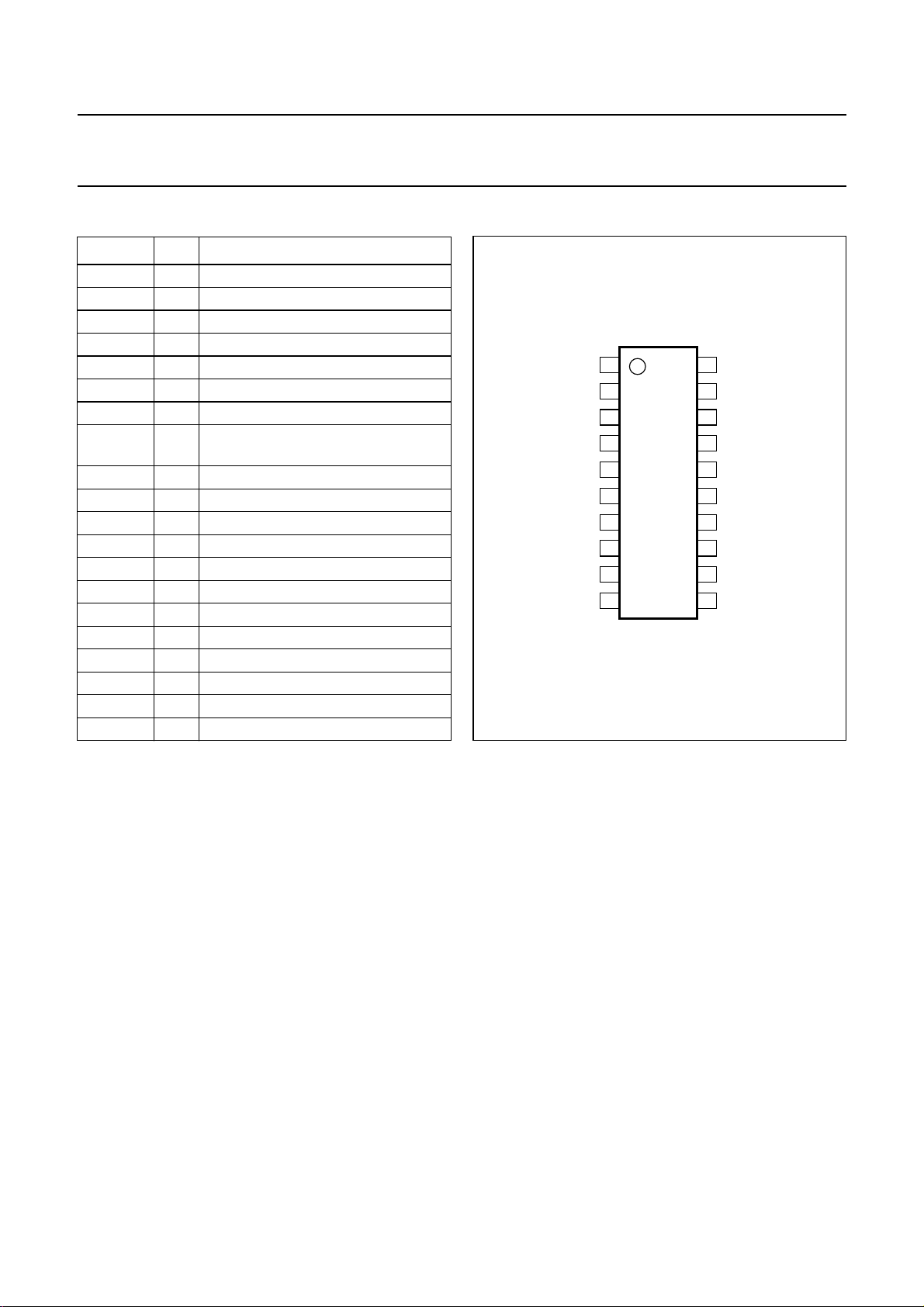
ORDERING INFORMATION
TYPE NUMBER
NAME DESCRIPTION VERSION
TDA9809M SSOP20 plastic shrink small outline package; 20 leads; body width 5.3 mm SOT339-1
1998 Jan 08 2
PACKAGE
Page 3

Philips Semiconductors Preliminary specification
Single standard multimedia IF-PLL and FM
TDA9809M
radio demodulator
QUICK REFERENCE DATA
SYMBOL PARAMETER CONDITIONS MIN. TYP. MAX. UNIT
Supply (pin 19)
V
P
I
P
Television mode
V
i(VIF)(rms)
V
o(video)(p-p)
B
−3dB
S/N
W(video)
α
IM(0.92/1.1)
α
IM(2.76/3.3)
α
H(sup)
V
i(SIF)(rms)
V
o(audio)(rms)
THD
video
S/N
W(audio)
supply voltage 4.5 5 5.5 V
supply current TV mode 76 89 102 mA
radio mode 29 35 41 mA
power-down mode 5 8 11 mA
minimum vision IF input signal
−1 dB video at output − 60 100 µV
voltage (RMS value)
video output signal voltage
0.97 1.1 1.23 V
(peak-to-peak value)
−3 dB video bandwidth on pin 13 CL< 30 pF; RL> 1.5 kΩ;
78−MHz
AC load
weighted signal-to-noise ratio for
54 58 − dB
video
intermodulation attenuation at ‘blue’ f = 0.92 or 1.1 MHz 52 58 − dB
intermodulation attenuation at ‘blue’ f = 2.76 or 3.3 MHz 52 58 − dB
suppression of harmonics in video
35 40 − dB
signal
minimum sound IF input signal
−3 dB at intercarrier output − 30 70 µV
voltage (RMS value)
audio output signal voltage for FM
0.4 0.5 0.6 V
(RMS value)
total harmonic distortion for video − 0.5 1.0 %
weighted signal-to-noise ratio for
50 55 − dB
audio
Radio mode
V
i(RIF)(rms)
V
i(FM)(rms)
/log∆Vioutput voltage slope according to
∆V
LD
minimum radio IF input signal
voltage (RMS value)
minimum FM limiter input signal
voltage (RMS value)
d3< 60 dB intermodulation;
note 1
SN+
unweighted 26 dB=
-------------N
FM limiter input voltage
V
o(audio)(rms)
audio output signal voltage for radio
22.5 kHz modulation 200 250 300 mV
(peak-to-peak value)
THD
S/N
audio
W(audio)
total harmonic distortion for audio 22.5 kHz modulation − 0.5 1.0 %
weighted signal-to-noise ratio for
audio
22.5 kHz modulation;
15 kHz bandwidth
Note
is the ratio of the intermodulation product at 10.3 MHz to the level of V
1. d
3
1998 Jan 08 3
−−20 mV
− 100 −µV
− 50 − mV/dBµV
59 64 − dB
i(4)(max)(rms)
.
Page 4
This text is here in white to force landscape pages to be rotated correctly when browsing through the pdf in the Acrobat reader.This text is here in
_white to force landscape pages to be rotated correctly when browsing through the pdf in the Acrobat reader.This text is here inThis text is here in
white to force landscape pages to be rotated correctly when browsing through the pdf in the Acrobat reader. white to force landscape pages to be ...
1998 Jan 08 4
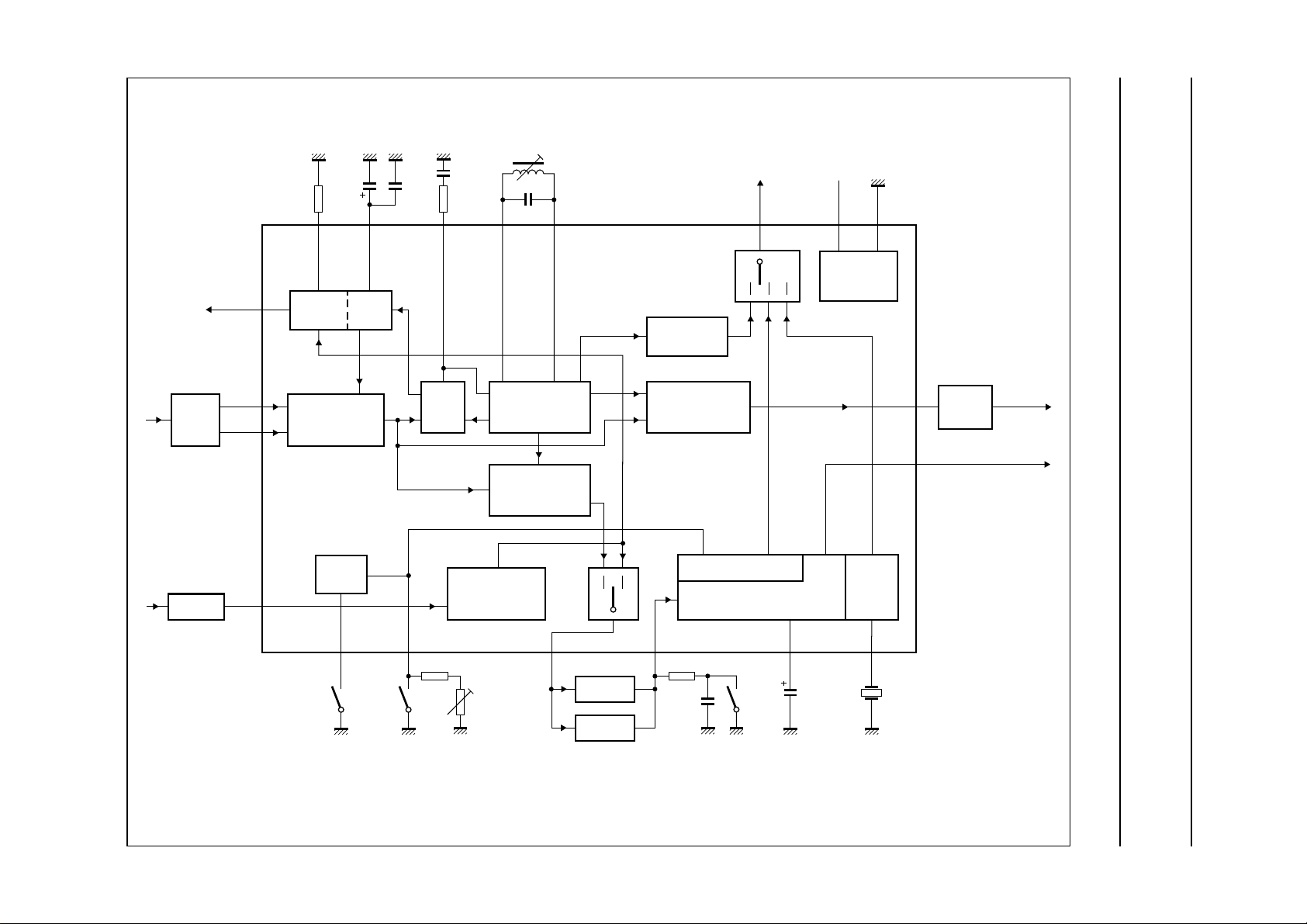
handbook, full pagewidth
BLOCK DIAGRAM
Single standard multimedia IF-PLL and FM
radio demodulator
Philips Semiconductors Preliminary specification
TV/radio
tuner AGC
VIF
SAW
10.7 MHz
TAGC
V
iVIF1
V
iVIF2
V
iRIF
TADJ
12
TUNER
AGC
1
VIF AMPLIFIER
2
AGC DETECTOR
4
AND
LOGIC
C
VAGC
VIF
AGC
T
PLL
FPLL
RIF AMPLIFIER
AGC DETECTOR
2 × f
PC
VCO
TWD
AND TV AFC
INTERCARRIER
MIXER
AND
AFC/RIF
level
14 1916156520 17
TV AFC
DETECTOR
VIDEO
DEMODULATOR
AND AMPLIFIER
TDA9809M
LEVEL DETECTOR
FM-PLL DEMODULATOR AND
AF SIGNAL PROCESSING
GNDV
P
INTERNAL
VOLTAGE
STABILIZER
RADIO
AFC
13
7
SOUND
TRAP
1.1 V (p-p)
video
1 V (p-p)
V
oAF
3
LP0
8
LP2
soft mute
threshold
adjust
V
o(int)
4.5 MHz
10.7 MHz
Fig.1 Block diagram.
9181110
V
iFM
forced
mute
C
DEC
10.7 MHz
ceramic
resonator
MHA957
TDA9809M
Page 5
Philips Semiconductors Preliminary specification
Single standard multimedia IF-PLL and FM
radio demodulator
PINNING
SYMBOL PIN DESCRIPTION
V
iVIF1
V
iVIF2
LP0 3 logic port 0
V
iRIF
C
VAGC
T
PLL
V
oAF
LP2
C
DEC
V
o(int)
V
iFM
TAGC 12 TV/radio tuner AGC output
V
o(vid)
AFC 14 AFC/RIF level output
VCO1 15 VCO1 resonance circuit
VCO2 16 VCO2 resonance circuit
GND 17 ground
CERRES 18 ceramic resonator 10.7 MHz
V
P
TADJ 20 tuner AGC takeover point adjustment
1 VIF differential input signal voltage 1
2 VIF differential input signal voltage 2
4 RIF input
5 VIF AGC capacitor
6 PLL loop filter
7 audio output
logic port 2 and soft mute threshold
8
adjustment
9 decoupling capacitor
10 intercarrier output voltage
11 sound intercarrier input voltage
13 composite video output voltage
19 supply voltage
handbook, halfpage
V
1
iVIF1
V
2
iVIF2
LP0
3
V
4
iRIF
C
VAGC
T
PLL
V
oAF
LP2
C
DEC
V
o(int)
5
TDA9809M
6
7
8
9
10
MHA958
Fig.2 Pin configuration.
TDA9809M
TADJ
20
19
V
P
18
CERRES
17
GND
16
VCO2
VCO1
15
AFC
14
V
13
o(vid)
TAGC
12
V
11
iFM
FUNCTIONAL DESCRIPTION
The TDA9809M is comprised of the functional blocks
shown in Fig.1:
• Vision IF amplifier and AGC detector
• Tuner (TV/radio) and VIF AGC
• Frequency Phase-Locked Loop (FPLL) detector
• VCO, Travelling Wave Divider (TWD) and TV AFC
• Video demodulator and amplifier
• Intercarrier mixer
• RIF amplifier and AGC detector
• FM-PLL demodulator, level detector and radio AFC
• Audio Frequency (AF) signal processing
• Internal voltage stabilizer
• Logic.
1998 Jan 08 5
Vision IF amplifier and AGC detector
The vision IF amplifier contains three AC-coupled
differential amplifier stages. Each differential stage
includes a feedback network controlled by emitter
degeneration.
The AGC detector generates the required VIF gain control
voltage for constant video output by charging/discharging
the AGC capacitor. The sync level of the video signal is
therefore detected for negative video modulation.
Tuner (TV/radio) and VIF AGC
For TV operation, the AGC capacitor voltage is converted
to an internal IF control signal and then fed to the tuner
AGC to generate the tuner AGC output current at
pin TAGC (open-collector output). The tuner AGC
takeover point can be adjusted at pin TADJ. This allows
the tuner to be matched to the SAW filter in order to
achieve the optimum IF input level.
For FM radio operation, an AGC detector is provided to
obtain some adjacent channel protection.
Page 6

Philips Semiconductors Preliminary specification
Single standard multimedia IF-PLL and FM
radio demodulator
Frequency Phased-Locked Loop detector (FPLL)
The VIF amplifier output signal is fed, via a limiting
amplifier, to a frequency and phase detector. During
acquisition, the frequency detector generates a DC current
that is proportional to the difference in frequency between
the input signal and the VCO signal.
After frequency lock-in, the phase detector generates a
DC current proportional to the phase difference between
the input signal and the VCO signal. The DC current
generated by the frequency or phase detector is converted
to a DC voltage via the loop filter, which controls the VCO
frequency.
VCO, TWD and TV AFC
The VCO operates with a resonance circuit (with L and C
in parallel) at double the Picture Carrier (PC) frequency.
The VCO is controlled by two integrated variable
capacitors. The control voltage required to tune the VCO
from its free-running frequency to double the PC frequency
is generated by the FPLL and fed via the loop filter to the
first variable capacitor. This control voltage is amplified
and converted into a current which represents the AFC
output signal. At the centre frequency, the AFC output
current is zero.
The TWD divides the oscillator signal by 2 and generates
two differential output signals with a 90° phase difference
independent of frequency.
TDA9809M
Intercarrier mixer
The intercarrier mixer is realized by a multiplier.
The sound IF signal passes through the vision IF SAW
filter and the composite IF signal is then fed to the
intercarrier mixer. Here, the IF signal is multiplied by the
90° TWD output signal to convert the sound IF to the
intercarrier frequency. By using this quadrature detection,
the low frequency video signals are removed. The mixer
output signal is fed, via a high-pass filter used to attenuate
the video signal components, at output pin 10.
RIF amplifier and AGC detector
The radio IF amplifier amplifies the 10.7 MHz radio IF
signal. This signal is supplied by the tuner and is fed to the
RIF input (pin 4) via a matching circuit and a ceramic
band-pass filter. This amplifier contains two stages.
The first stage, a conventional 0 dB differential amplifier
designed for optimal dynamic range, is followed by a
switchable differential amplifier stage with a gain of 10 dB.
Either the radio IF or the TV IF signal can be selected at
the output (pin 10).
The RIF output signal is fed via ceramic band-pass filters
to the FM-PLL demodulator and the radio IF AGC detector.
The AGC threshold is very high and is designed to obtain
some adjacent channel protection. The AGC detector
output is fed to the tuner AGC output stage (pin 12) to
control the tuner.
Video demodulator and amplifier
Video demodulation is realized by a multiplier designed for
low distortion and wide bandwidth. The vision IF input
signal and the ‘in-phase’ signal of the travelling wave
divider output are multiplied together.
The demodulated output signal is fed to the video amplifier
via an integrated low-pass filter used to attenuate the
carrier harmonics. This is an operational amplifier with
internal feedback and wide bandwidth. A low-pass filter is
integrated to attenuate the carrier harmonics. The video
output signal at V
modulation, in order to achieve 1 V (p-p) at the sound trap
output.
1998 Jan 08 6
is 1.1 V (p-p) for nominal vision IF
o(vid)
FM-PLL demodulator, level detector and radio AFC
The FM-PLL demodulator consists of a limiter and an FM
phase-locked loop. The 8-stage internally AC-coupled
limiter amplifies and limits the TV FM sound intercarrier or
the radio FM intermediate frequency signal prior to
demodulation. The limiter is designed for high sensitivity
and AM suppression with low DC offset and needs no
external pins for DC coupling.
Furthermore, the AF output signal can be force muted by
connecting a resistor between pin 11 and ground. The soft
mute function can be disabled by connecting a resistor
between pin 11 and the power supply. See the application
circuit in Fig.16.
Page 7

Philips Semiconductors Preliminary specification
Single standard multimedia IF-PLL and FM
radio demodulator
The FM-PLL consists of an integrated relaxation oscillator,
an integrated loop filter and a phase detector.
The oscillator is locked to the FM intercarrier signal output
from the limiter. As a result of locking, the oscillator
frequency tracks with the modulation of the input signal
and the oscillator control voltage is superimposed on the
AF voltage. The FM-PLL operates as an FM demodulator.
The level detector detects, rectifies and amplifies the
output signals from the first 5 limiter stages. These signals
are then summed and the composite signal passed
through a low-pass filter, followed by a 6 dB output
amplifier. A DC voltage dependent on the limiter input level
is generated for controlling the behaviour of the AF soft
mute. The 6 dB output amplifier can be switched off via the
control logic and the level detector output signal fed to
pin 14. Furthermore, the steepness of the level detector
output signal tracks that of the power supply voltage.
The radio Automatic Frequency Control (AFC) stage is
comprised of a 10.7 MHz phase shifting network, a phase
detector (quadrature demodulator), a differential amplifier
input stage (which receives the limiting amplifier output
signal) and a current mode output stage.
A ceramic resonator is used for phase shifting. This
permits alignment-free operation.
AF signal processing
TDA9809M
Soft mute occurs when the internal level detector output
voltage is lower than the mute threshold voltage at pin 8
(provided an external resistor is not connected between
the limiter input, pin 11, and the supply voltage). The mute
stage reduces the AF signal by 25 dB, with an internal time
constant of approximately 7 ms.
If a resistor is connected between pin 11 and ground
(forced mute), the mute stage will reduce the AF signal by
more than 70 dB with the same time constant.
Otherwise, the AF signal will not be reduced.
The AF post-amplifier, which was designed to include a
rail-to-rail output stage, provides the required AF output
level at pin 7.
Internal voltage stabilizer
The bandgap circuit generates a voltage of approximately
1.25 V internally, independent of supply voltage and
temperature. A voltage regulator circuit connected to this
voltage generates a constant 3.6 V which is used as an
internal reference voltage.
Logic
The logic circuit detects the logic levels and threshold
voltages at ports LP0 and LP2 and controls the internal
functions as described in Table 2.
The AF signal processing stage consists of a pre-amplifier
for the FM-PLL demodulator output signal, an AF source
selector, a soft and forced mute stage with an integrated
time constant and an AF post-amplifier.
The FM demodulator output signal is pre-amplified by an
operational amplifier (30 dB gain) with internal feedback,
high gain and high common mode rejection. The feedback
circuit, together with external capacitor C
pin 9, keeps the DC level at the pre-amplifier output
constant (2.3 V). An external resistor connected in series
with C
The low-pass filter characteristic (130 kHz bandwidth) of
the amplifier reduces the harmonics of the IF signal at the
sound signal output.
provides a gain reduction capability.
DEC
connected to
DEC
1998 Jan 08 7
Page 8
Philips Semiconductors Preliminary specification
Single standard multimedia IF-PLL and FM
TDA9809M
radio demodulator
LIMITING VALUES
In accordance with the Absolute Maximum Rating System (IEC 134).
SYMBOL PARAMETER CONDITIONS MIN. MAX. UNIT
V
P
V
n
t
sc
V
TAGC
T
stg
T
amb
V
es
Notes
1. I
= 102 mA; T
P
2. Machine model class B (L = 2.5 µH).
supply voltage (pin 19) maximum chip temperature of
− 5.5 V
130 °C; note 1
input voltage at pins 1 to 9, 11, 12, 14
0V
P
and 17 to 20
short-circuit time − 10 s
tuner AGC output voltage 0 13.2 V
storage temperature −25 +150 °C
ambient operating temperature −20 +70 °C
electrostatic handling note 2 −300 +300 V
=70°C; R
amb
th(j-a)
= 120 K/W.
V
THERMAL CHARACTERISTICS
SYMBOL PARAMETER CONDITIONS VALUE UNIT
R
th(j-a)
thermal resistance from junction to ambient in free air 120 K/W
CHARACTERISTICS
=5V; T
V
P
V
i(FM)(rms)
B/G: 10%; video signal in accordance with
=25°C; see Table 1 for input frequencies; input level V
amb
i(VIF)(rms)
= 10 mV (sync-level for B/G);
= 10 mV; IF input from 50 Ω via broadband transformer 1 : 1; video modulation DSB; residual carrier
“CCIR, line 17”
or
“NTC-7 Composite”
; test circuit in Fig.15 used for
measurements; unless otherwise specified.
SYMBOL PARAMETER CONDITIONS MIN. TYP. MAX. UNIT
Supply (pin 19)
V
P
I
P
supply voltage note 1 4.5 5 5.5 V
supply current TV mode 76 89 102 mA
radio mode 29 35 41 mA
power-down mode 5 8 11 mA
Television mode
V
ISION IF AMPLIFIER (PINS 1 AND 2)
V
i(VIF)(rms)
minimum vision IF
input signal voltage
fPC= 38.9 or 45.75 MHz;
−1 dB video at output
− 60 100 µV
(RMS value)
maximum vision IF
input signal voltage
= 38.9 or 45.75 MHz;
f
PC
+1 dB video at output
120 200 − mV
(RMS value)
1998 Jan 08 8
Page 9

Philips Semiconductors Preliminary specification
Single standard multimedia IF-PLL and FM
TDA9809M
radio demodulator
SYMBOL PARAMETER CONDITIONS MIN. TYP. MAX. UNIT
∆V
o(int)
G
VIF(CR)
B
VIF(−3dB)
R
i(dif)
C
i(dif)
V
I
TRUE SYNCHRONOUS VIDEO DEMODULATOR; note 3
f
VCO(max)
/∆T oscillator drift as a
∆f
osc
V
VCO(rms)
f
cr(PC)
t
acq
V
i(VIF)(rms)
COMPOSITE VIDEO AMPLIFIER (PIN 13; SOUND CARRIER OFF)
V
o(video)(p-p)
V/S ratio of video
V
sync
V
clu
V
cll
R
o
internal IF amplitude
difference between
within AGC range;
∆f = 4.5 MHz
− 0.7 1 dB
picture and sound
carrier
VIF gain control range see Fig.3 65 70 − dB
−3 dB VIF bandwidth lower limit − 15 25 MHz
upper limit 70 100 − MHz
differential input
note 2 1.7 2.2 2.7 kΩ
resistance
differential input
note 2 1.2 1.7 2.5 pF
capacitance
DC input voltage note 2 − 3.4 − V
maximum oscillator
f=2f
PC
125 130 − MHz
frequency for carrier
regeneration
−6K−1
function of
oscillator is free-running;
I
= 0; note 4
AFC
−−±20 × 10
temperature
oscillator voltage
swing at
pins 15 and 16
fPC= 38.9 MHz 50 80 110 mV
f
= 45.75 MHz 40 65 90 mV
PC
(RMS value)
picture carrier capture
±1.4 ±1.8 − MHz
range
acquisition time Black Level (BL) = 70 kHz
−−30 ms
note 5
minimum vision IF
maximum IF gain; note 6 − 30 70 µV
input signal voltage for
PLL to be locked
(RMS value)
output signal voltage
see Fig.7 0.97 1.1 1.23 V
(peak-to-peak value)
1.9 2.33 3.0 −
(black-to-white) to
sync level
sync voltage level 1.4 1.5 1.6 V
upper video clipping
VP− 1.1 VP− 1 − V
voltage level
lower video clipping
− 0.7 0.9 V
voltage level
output resistance note 2 −−10 Ω
1998 Jan 08 9
Page 10

Philips Semiconductors Preliminary specification
Single standard multimedia IF-PLL and FM
TDA9809M
radio demodulator
SYMBOL P ARAMETER CONDITIONS MIN. TYP. MAX. UNIT
I
bias(int)
I
o(sink)(max)
I
o(source)(max)
∆V
o(CVBS)
∆V
o(bl)(BG)
G
dif
ϕ
dif
B
v(−1dB)
B
v(−3dB)
S/N
W
S/N unweighted
α
IM(0.92/1.1)
α
IM(2.76/3.3)
α
r(vc)(rms)
α
H(sup)
α
H(spur)
PSRR power supply ripple
internal DC bias
current for
emitter-follower
maximum AC and DC
output sink current
maximum AC and DC
output source current
deviation of CVBS
output signal voltage
black level tilt in B/G
50 dB gain control −−0.5 dB
30 dB gain control −−0.1 dB
gain variation; note 7 −−1%
standard
differential gain
“CCIR, line 330”
or
“NTC-7 Composite”
differential phase
“CCIR, line 330”
or
“NTC-7 Composite”
−1 dB video bandwidth CL< 50 pF; RL>1kΩ;
AC load
−3 dB video bandwidth CL< 50 pF; RL>1kΩ;
AC load
weighted
see Fig.4 and note 8 54 58 − dB
signal-to-noise ratio
see Fig.4 and note 8 47 51 − dB
signal-to-noise ratio
intermodulation
attenuation at ‘blue’
intermodulation
attenuation at ‘yellow’
intermodulation
attenuation at ‘blue’
intermodulation
attenuation at ‘yellow’
residual vision carrier
(RMS value)
harmonics
fIM= 0.92 or 1.1 MHz;
see Fig.5 and note 9
= 0.92 or 1.1 MHz;
f
IM
see Fig.5 and note 9
fIM= 2.76 or 3.3 MHz;
see Fig.5 and note 9
f
= 2.76 or 3.3 MHz;
IM
see Fig.5 and note 9
fundamental wave and
harmonics
note 10a 35 40 − dB
suppression in video
signal
spurious element
note 10b 40 −− dB
suppression
video signal; grey level; see
rejection at pin 13
Fig.9
2.2 3.0 − mA
1.6 −− mA
2.9 −− mA
− 25 %
− 2 4 deg
56− MHz
78− MHz
52 58 − dB
54 60 − dB
52 58 − dB
54 60 − dB
− 25 mV
30 35 − dB
1998 Jan 08 10
Page 11

Philips Semiconductors Preliminary specification
Single standard multimedia IF-PLL and FM
TDA9809M
radio demodulator
SYMBOL PARAMETER CONDITIONS MIN. TYP. MAX. UNIT
VIF-AGC DETECTOR (PIN 5)
I
ch
I
dch
t
res(AGC)(r)
t
res(AGC)(f)
TV TUNER AGC (PIN 12)
V
i(rms)
V
o(max)
V
sat
∆V
/∆T variation of takeover
TOP
I
sink
∆G
IF
TV AFC DETECTOR (PIN 14); see Fig.6 and note 12
CR
stps
∆f
/∆T frequency variation
IF
V
o(max)
V
o(min)
I
o(source)
I
o(sink)
∆I
r(mod)(p-p)
charge current note 7 0.75 1 1.25 mA
discharge current 15 20 25 µA
AGC response time to
note 11 − 0.05 0.1 ms/dB
a rising VIF step
AGC response time to
− 2.2 3.5 ms/dB
a falling VIF step
IF input signal voltage
for minimum onset of
input at pins 1 and 2;
R
=22kΩ; I12= 0.4 mA
TOP
− 25 mV
tuner takeover
(RMS value)
IF input signal voltage
for maximum onset of
input at pins 1 and 2;
R
=0Ω; I12= 0.4 mA
TOP
50 100 − mV
tuner takeover
(RMS value)
tuner takeover point
=13kΩ; I12= 0.4 mA 5 − 20 mV
R
TOP
accuracy (RMS value)
maximum output
voltage
from external source;
note 2
−−13.2 V
saturation voltage I12= 1.5 mA −−0.2 V
I12= 0.4 mA − 0.03 0.07 dB/K
point with temperature
sink current see Fig.3
no tuner gain reduction;
V
= 13.2 V
12
maximum tuner gain
−−1 µA
1.5 2 2.6 mA
reduction
IF slip by automatic
gain control
control steepness
∆I14/∆f
tuner gain current from
− 68 dB
20 to 80%
fPC= 38.9 MHz; note 13 0.5 0.75 1.0 µA/kHz
= 45.75 MHz; note 13 0.4 0.65 0.9 µA/kHz
f
PC
I
= 0; note 4 −−±20 × 10
AFC
−6K−1
with temperature
output voltage upper
limit
output voltage lower
see Fig.6 without external
components
VP− 0.6 VP− 0.3 − V
− 0.3 0.6 V
limit
output source current 150 200 250 µA
output sink current 150 200 250 µA
residual video
− 20 30 µA
modulation current
(peak-to-peak value)
1998 Jan 08 11
Page 12

Philips Semiconductors Preliminary specification
Single standard multimedia IF-PLL and FM
TDA9809M
radio demodulator
SYMBOL PARAMETER CONDITIONS MIN. TYP. MAX. UNIT
INTERCARRIER MIXER (PIN 10)
V
o(intercarrier)(rms)
IF intercarrier level
(RMS value)
B
−3dB
−3 dB intercarrier
bandwidth
α
r(SC)(rms)
residual sound carrier
(RMS value)
α
r(VC)(rms)
residual vision carrier
(RMS value)
α
H(sup)
suppression of video
signal harmonics
R
o
V
O
I
bias(int)
output resistance note 2 − 25 −Ω
DC output voltage − 2.0 − V
DC internal bias
current for
emitter-follower
I
o(sink)(max)
maximum AC and DC
output sink current
I
o(source)(max)
maximum AC and DC
output source current
LIMITER AMPLIFIER (PIN 11); note 15
V
i(FM)(rms)
input signal voltage for
lock-in (RMS value)
input signal voltage
(RMS value)
allowed input signal
voltage (RMS value)
α
AM
R
i
V
I
AM suppression 50 µs de-emphasis;
input resistance note 2 480 600 720 Ω
DC input voltage − 2.65 − V
FM-PLL DEMODULATOR
f
cr(PLL)
f
hr(PLL)
t
acq
catching range of PLL upper limit 7.0 −− MHz
holding range of PLL upper limit 9.0 −− MHz
acquisition time −−4 µs
sound carrier 1 (SC1);
− 32 − mV
SC2off; note 14
upper limit 7.5 9 − MHz
fundamental wave and
− 25 mV
harmonics
fundamental wave and
− 25 mV
harmonics
intercarrier mode;
f
≤ 5 MHz
video
39 −− dB
2.7 3.4 − mA
1.5 2.0 − mA
2.5 −− mA
−−100 µV
SN+
-------------N
weighted 40 dB=
− 250 500 µV
200 −− mV
46 50 − dB
AM: f
= 1 kHz; m = 0.3
mod
referenced to 27 kHz
(54% FM deviation)
lower limit −−4.0 MHz
lower limit −−3.5 MHz
1998 Jan 08 12
Page 13

Philips Semiconductors Preliminary specification
Single standard multimedia IF-PLL and FM
TDA9809M
radio demodulator
SYMBOL PARAMETER CONDITIONS MIN. TYP. MAX. UNIT
FM OPERATION (PIN 7); notes 15 and 15a
V
o(AF)(rms)
AF output signal
voltage (RMS value)
V
o(AF)(cl)(rms)
AF output clipping
signal voltage level
(RMS value)
∆f
AF
∆V
/∆T temperature drift of AF
o
frequency deviation THD < 1.5%; note 16 −−±53 kHz
output signal voltage
V
9
DC voltage at
decoupling capacitor
R
o
V
O
I
o(sink)(max)
output resistance note 2 −−150 Ω
DC output voltage − 2.3 − V
maximum AC and DC
output sink current
I
o(source)(max)
maximum AC and DC
output source current
B
aud(−3dB)
−3 dB audio
frequency bandwidth
THD total harmonic
distortion
S/N
W
weighted
signal-to-noise ratio
α
r(SC)(rms)
residual sound carrier
(RMS value)
α
mute(AF)
mute attenuation of AF
signal
∆V
7
DC jump voltage of AF
output terminal for
switching AF output to
mute state and vice
versa
PSRR power supply ripple
rejection at pin 7
Rx=0Ω; see Fig.15 and
note 16
27 kHz
400 500 600 mV
(54% FM deviation)
25 kHz
360 460 560 mV
(50% FM deviation)
THD < 1.5% 1.0 − 1.2 V
−3
voltage dependent on VCO
− 3 × 10−37 × 10
1.2 − 3.0 V
frequency; note 17
−−0.5 mA
−−0.5 mA
100 125 − kHz
27 kHz (54% FM deviation) − 0.5 1.0 %
FM-PLL only; with 50 µs
50 55 − dB
de-emphasis; 27 kHz
(54% FM deviation);
“CCIR 468-4”
fundamental wave and
; see Fig.8
−−75 mV
harmonics
70 75 − dB
FM-PLL in lock mode −±50 ±150 mV
R
x
=0Ω; f
mod
= 70 Hz;
20 26 − dB
see Figs 9 and 15
dB/K
1998 Jan 08 13
Page 14

Philips Semiconductors Preliminary specification
Single standard multimedia IF-PLL and FM
TDA9809M
radio demodulator
SYMBOL PARAMETER CONDITIONS MIN. TYP. MAX. UNIT
INTERCARRIER AF PERFORMANCE FOR FM OPERATION; notes 18, 19 and 20; see Table 1
S/N
W(SC1)
weighted
signal-to-noise ratio
for SC
1
Radio mode
RIF
AMPLIFIER (PINS 4 AND 10)
V
i(4)(max)(rms)
maximum input signal
voltage (RMS value)
V
o(10)(cl)(rms)
RF amplifier output
clipping signal voltage
level (RMS value)
G
RIF
B
RIF(−3dB)
R
i(SE)
RIF gain 10 13 16 dB
−3 dB RIF bandwidth lower limit − 100 − kHz
single-ended input
resistance
C
i(SE)
single-ended input
capacitance
R
o
V
I(4)
output resistance note 2 − 25 −Ω
DC input voltage note 2 − 2.7 − V
RADIO TUNER AGC (PIN 12)
I
sink
V
o(max)
sink current maximum tuner gain
maximum output
voltage
V
o(10)(rms)
AGC onset
(RMS value)
PC/SC1 ratio at pins 1
27 −− dB
and 2; 27 kHz (54% FM
deviation);
“CCIR 468-4”
;
50 µs (75 µs at M standard)
black picture 41 47 − dB
white picture 41 47 − dB
6 kHz sine wave
35 40 − dB
(black-to-white
modulation)
sound carrier
30 35 − dB
subharmonics;
f
= 2.75 MHz ±3 kHz
mod
d3<60dB
10 20 − mV
intermodulation;
notes 21 and 22
−1 dB gain compression
400 − 900 mV
point; note 21
upper limit − 25 − MHz
note 2 240 330 420 Ω
note 2 1.5 2 2.5 pF
1.5 2 2.6 mA
reduction
from external source;
−−13.2 V
note 2
RIF amplifier output;
− 180 − mV
I12= 0.4 mA
1998 Jan 08 14
Page 15

Philips Semiconductors Preliminary specification
Single standard multimedia IF-PLL and FM
TDA9809M
radio demodulator
SYMBOL PARAMETER CONDITIONS MIN. TYP. MAX. UNIT
RADIO AFC DETECTOR (PIN 14); see Fig.11 and note 12a
CR
stps
control steepness
∆I14/∆f
∆f
IF
frequency variation by
input level
V
o(max)
output voltage upper
limit
V
o(min)
output voltage lower
limit
I
o(source)
I
o(sink)
output source current 150 200 250 µA
output sink current 150 200 250 µA
LIMITER AMPLIFIER (PIN 11); note 15
V
i(FM)(rms)
input signal voltage
(RMS value)
allowed input signal
voltage (RMS value)
α
AM
R
i
V
I
AM suppression 50 µs de-emphasis;
input resistance note 2 240 330 420 Ω
DC input voltage − 2.65 − V
LEVEL DETECTOR (PIN 14); note 12
∆V
/log ∆V
LD
output voltage slope
i
according to FM limiter
input voltage
V
O(LD)(min)
minimum DC output
voltage
V
O(LD)
V
O(LD)(max)
DC output voltage V
maximum DC output
voltage
∆V
O
/∆V
P
output voltage
variation with V
∆V
/∆T output voltage
O
variation with
temperature
FM-PLL DEMODULATORS
f
cr(PLL)
f
hr(PLL)
t
acq
catching range of PLL upper limit 11.5 −− MHz
holding range of PLL upper limit 13.0 −− MHz
acquisition time −−4 µs
P
note 23 0.59 0.9 1.22 µA/kHz
note 2 −−50 × 10
see Fig.11 without external
VP− 0.6 VP− 0.3 − V
−6
components
− 0.3 0.6 V
−3 dB AF signal at pin 7 − 50 −µV
∆f = 22.5 kHz;
SN+
unweighted 26 dB=
-------------N
− 100 −µV
200 −− mV
40 45 − dB
AM: f
= 1 kHz; m = 0.3
mod
referenced to 22.5 kHz
− 50 − mV/dBµV
V
=56µV (35 dBµV) 0 − 1.0 V
i(11)
= 32 mV (90 dBµV) − 3.00 − V
i(11)
−−V
−1.0 V
P
0.5 0.7 0.9 V/V
−−±100 × 10−6V/K
lower limit −−9.0 MHz
lower limit −−8.0 MHz
(dBµV)
−1
1998 Jan 08 15
Page 16

Philips Semiconductors Preliminary specification
Single standard multimedia IF-PLL and FM
TDA9809M
radio demodulator
SYMBOL PARAMETER CONDITIONS MIN. TYP. MAX. UNIT
FM OPERATION (PIN 7); notes 15 and 15a
V
o(AF)(rms)
AF output signal
voltage (RMS value)
V
o(AF)(cl)(rms)
AF output clipping
signal voltage level
(RMS value)
∆f
AF
∆V
/∆T temperature drift of AF
o
frequency deviation THD < 1.5%; note 16 −−±75 kHz
output signal voltage
V
9
DC voltage at
decoupling capacitor
R
o
V
O
I
o(sink)(max)
output resistance note 2 −−150 Ω
DC output voltage − 2.3 − V
maximum AC and DC
output sink current
I
o(source)(max)
maximum AC and DC
output source current
B
AF(−3dB)
−3 dB AF bandwidth 22.5 kHz 100 125 − kHz
THD total harmonic
distortion
S/N unweighted
signal-to-noise ratio
∆V
7
DC jump voltage of AF
output terminal for
switching AF output to
mute state and vice
versa
PSRR power supply ripple
rejection at pin 7
MUTE BEHAVIOUR; note 15
α
mute
forced mute
attenuation
soft mute attenuation RIF level dependent;
I
11(forced)
forced mute switching
current
I
11(soft)(dis)
current for disabling
soft mute
V
th(8)
soft mute threshold
adjustment voltage
t
mute
time constant mute on or off 3 − 7ms
22.5 kHz; Rx=0Ω;
200 250 300 mV
see Fig.15 and note 16
THD < 1.5% 1.0 − 1.2 V
−3
voltage dependent on VCO
− 3 × 10−37 × 10
1.2 − 3.0 V
frequency; note 17
−−0.5 mA
−−0.5 mA
22.5 kHz − 0.5 1.0 %
FM-PLL only; with 50 µs
59 64 − dB
de-emphasis; 22.5 kHz;
15 kHz bandwidth
FM-PLL in lock mode −±50 ±150 mV
R
=0Ω; f
x
mod
= 70 Hz;
20 26 − dB
see Figs 9 and 15
pin 11 at V
P
70 75 − dB
20 25 30 dB
see Fig.12
α7>70dB − 350 −µA
α7>0dB −−350 −µA
V
=56µV 0.8 1.0 1.2 V
i(11)
V
= 560 µV 1.2 1.4 1.6 V
i(11)
dB/K
1998 Jan 08 16
Page 17

Philips Semiconductors Preliminary specification
Single standard multimedia IF-PLL and FM
TDA9809M
radio demodulator
SYMBOL PARAMETER CONDITIONS MIN. TYP. MAX. UNIT
Switching levels for logic port 0; see also Table 2
V
logic
DC potential for logic 1
or pin not connected
DC potential for logic 0 0 − 0.8 V
I
IL
LOW-level input
V
=0V 507090 µA
3,8
current
Switching levels for logic port 2; see also Table 2 and Fig.12
V
logic
DC potential for logic 1
or pin not connected
DC potential for logic 0 0 − 0.8 V
I
IL
LOW-level input
V11= 0 V 110 150 190 µA
current
Notes
1. Video and sound parameters are degraded at VP≤ 4.5 V.
2. This parameter is not tested during production and is provided as application information for use in designing the
television receiver.
3. Loop bandwidth BL = 70 kHz (natural frequency fn= 12 kHz; damping factor d ≈ 3; calculated for peak level).
Resonance circuit of VCO: Q0> 50; C
= 8.2 pF ± 0.25 pF; C
VCO
4. Temperature coefficient of external LC circuit is equal to zero.
5. V
i(VIF)(rms)
=10mV;∆f = 1 MHz (VCO frequency offset related to picture carrier frequency); white picture
video modulation.
6. V
signal for nominal video signal.
i(VIF)
7. The leakage current of the AGC capacitor should not exceed 1 µA to avoid larger tilt.
8. S/N is the ratio of black-to-white amplitude to the black level noise voltage (RMS value, pin 13). B = 5 MHz weighted
in accordance with
“CCIR 567”
.
9. The intermodulation figures are defined:
at 3.58 (4.4) MHz
V
0
α
IM(0.92/1.1)
20
------------------------------------------------------at 0.92 (1.1) MHz
V
0
3.6 dB+log=
; α
IM(0.92/1.1)
black/white signal;
α
IM(2.76/3.3)
20
log=
------------------------------------------------------at 2.76 (3.3) MHz
V
0
; α
IM(2.76/3.3)
value at 2.76 or 3.3 MHz referenced to colour carrier.
V
at 3.58 (4.4) MHz
0
10. Measurements taken with SAW filter G1962 (sound shelf: 20 dB); loop bandwidth = 70 kHz.
a) Modulation VSB; sound carrier off; f
b) Sound carrier on; SIF SAW filter K9453; f
video
> 0.5 MHz.
= 10 kHz to 10 MHz.
video
11. Response speed valid for a VIF input level range of 200 µVupto70mV.
12. A current source output is provided to match the AFC output signal to different tuning systems. The test circuit is
given in Fig.6 for TV mode and in Fig.11 for radio mode. The AFC steepness can be changed by the resistors at
pin 14.
a) A voltage output is provided to match the AFC output signal to different tuning systems. The DC load current
should not exceed 180 µA.
13. Depending on the ratio ∆C/C0 of the LC resonant circuit of the VCO (Q0> 50; see note 3; C0=C
2.8 − V
0.8 − V
≈ 8.5 pF (loop voltage ≈ 2.7 V).
int
P
P
value at 0.92 or 1.1 MHz referenced to
int+Cext
V
V
).
1998 Jan 08 17
Page 18

Philips Semiconductors Preliminary specification
Single standard multimedia IF-PLL and FM
TDA9809M
radio demodulator
14. The intercarrier output signal at pin 10 can be calculated with the following formula using the video output signal at
pin 13 (V
V
with = correction term for RMS value,
o(video)(p-p)
o rms()
1
---------- -
1.1 V p p–()
22
V
i(SC)
-------------V
i(PC)
= sound-to-picture carrier ratio at VIF input (pins 1 and 2) in dB,
(dB)
6 dB = correction term of internal circuitry and ±3 dB = tolerance of video output and intercarrier output amplitude
V
.
o(rms)
Example: SAW filter G1962 (sound shelf: 20 dB) .
15. Input level for second IF from an external generator with 50 Ω source impedance. AC-coupled with 10 nF capacitor,
f
= 1 kHz, 27 kHz (54% FM deviation) of audio reference. A VIF/SIF input signal is not permitted. Pin 5 has to be
mod
connected to the positive supply voltage for minimum IF gain. S/N and THD measurements are taken at 50 µs (75 µs
at M standard) de-emphasis (modulator pre-emphasis has to be activated). The FM demodulator steepness
∆V
/∆fAF is positive.
o(AF)
a) Second IF input level 10 mV (RMS).
16. Measured with an FM deviation of 27 kHz, the typical AF output signal is 500 mV (RMS) (Rx=0Ω). By using
Rx= 680 Ω the AF output signal is attenuated by 6 dB (250 mV RMS). For handling a frequency deviation of more
than 53 kHz the AF output signal has to be reduced by using Rx in order to avoid clipping (THD < 1.5%). For an
FM deviation up to 100 kHz an attenuation of 6 dB is recommended with Rx= 680 Ω.
17. The leakage current of the decoupling capacitor (2.2 µF) should not exceed 1 µA.
18. For all S/N measurements, the vision IF modulator used must meet the following specifications:
a) Incidental phase modulation for black-to-white jump less than 0.5 degrees.
b) QSS AF performance, measured with the television-demodulator AMF2 (audio output, weighted S/N ratio) better
than 60 dB (deviation ±27 kHz) for 6 kHz sine wave black-to-white video modulation.
c) Picture-to-sound carrier ratio; PC/SC1= 13 dB; (transmitter).
19. The PC/SC1 ratio at pins 1 and 2 is calculated as the addition of TV transmitter PC/SC1 ratio and SAW filter PC/SC
ratio. This PC/SC1 ratio is necessary to achieve the S/NW values as noted. A different PC/SC1 ratio will change
these values.
20. Measurements taken with SAW filter G1962 (sound shelf: 20 dB) for vision and sound IF.
21. The RIF amplifier output (pin 10) must be connected to a multistandard application ceramic filter for
5.5, 6.0 and 10.7 MHz. This total load constitutes an impedance of 250 Ω.
22. d3 tested using two signals with frequencies of f1= 10.5 MHz and f2= 10.7 MHz, and with a level of V
each signal. d3 is the ratio of the intermodulation product at 10.3 MHz to the output level of V
23. The control steepness of the radio AFC detector is dependent on the characteristic of the ceramic resonator, pin 18.
The figure given here will be obtained when applying a typical resonator of the type CDA 10.7 MC1-A (Murata).
The spread of the control steepness depends on the spread of the ceramic resonator characteristic (see Fig.11).
= 1.1 V typical) as a reference:
V
iSC()
dB()6dB3dB±+
---------------- V
iPC()
1
× 10
×=
---------- -
-------------------------------------------------------------------20
22
V
i(SC)
-------------V
i(PC)
27 dB– V
o(rms)
32 mV (typ.)=⇒=⇒
i(4)(max)(rms)
i(4)(max)(rms)
.
for
1
1998 Jan 08 18
Page 19

Philips Semiconductors Preliminary specification
Single standard multimedia IF-PLL and FM
TDA9809M
radio demodulator
Table 1 Input frequencies and carrier ratios
DESCRIPTION SYMBOL B/G STANDARD M/N STANDARD FM RADIO UNIT
Picture/IF carrier f
Sound carrier f
Picture-to-sound carrier PC/SC
or f
PC
SC1
f
SC2
PC/SC
IF
1
2
Table 2 Switch logic
FUNCTION LP2 LP0 REMARKS
Power-down 0 0
TV mode negative modulation 0 1
Radio mode AFC soft mute active 1 0 RIF level dependent (25 dB)
RIF level 1 1
handbook, full pagewidth
V
i(VIF)(rms)
(mV)
0.6
gain
(dB)
70
600.06
50
40
38.9 45.75 10.7 MHz
33.4 41.25 − MHz
33.158 −−MHz
13 7 − dB
20 −−dB
MHA959
I
tuner
(mA)
0
(1) I
tuner
(2) Gain.
; R
30
206
10
060
−10
1 2.521.5 3 3.5 4
TOP
=22kΩ.
(3) I
(4) I
tuner
tuner
; R
; R
TOP
TOP
=13kΩ.
=0Ω.
(1) (2) (3) (4)
Fig.3 Typical VIF and tuner AGC characteristic.
V5 (V)
1
2
4.5
1998 Jan 08 19
Page 20

Philips Semiconductors Preliminary specification
Single standard multimedia IF-PLL and FM
radio demodulator
70
handbook, halfpage
60
S/N
(dB)
50
40
30
20
10
0
−60 −40 −20 20
0.06 0.6 6 60060
10
V
i(VIF)(rms)
V
i(VIF)(rms)
Fig.4 Typical signal-to-noise ratio as a function of
IF input voltage.
MHA960
0
(dB)
(mV)
handbook, halfpage
13.2 dB
27 dB
SC CC PC SC CC PC
3.2 dB
13.2 dB
27 dB
BLUE YELLOW
SC = sound carrier, with respect to sync level.
CC = chrominance carrier, with respect to sync level.
PC = picture carrier, with respect to sync level.
The sound carrier levels are taking into account
a sound shelf attenuation of 20 dB (SAW filter G1962).
Fig.5 Input signal conditions.
TDA9809M
10 dB
MED685 - 1
handbook, full pagewidth
P
TDA9809M
14
VP = 5 VV
I
14
22 kΩ V
22 kΩ
100
nF
AFC
Fig.6 Measurement conditions and typical AFC characteristic for TV operation.
1998 Jan 08 20
V
AFC
(V)
2.5
I
14
(µA)
−200
−100
0
100
200
38.5 38.9 39.3
MHA961
(source current)
(sink current)
f (MHz)
Page 21

Philips Semiconductors Preliminary specification
Single standard multimedia IF-PLL and FM
radio demodulator
2.6 V
handbook, halfpage
1.83 V
1.5 V
B/G and M/N standard
white level
black level
sync level
MHA962
10
handbook, halfpage
(dB)
−10
−30
−50
−70
30
(1) Signal.
(2) AM rejection.
(3) Noise.
TDA9809M
MHA669
(1)
(2)
(3)
50
70 110
90
Vi (dBµV)
Fig.7 Typical video signal levels on output pin 13
(sound carrier off).
handbook, full pagewidth
VP = 5 V
TDA9809M
MHA963
VP = 5 V
Fig.8 Typical audio level, noise and AM rejection
(54% FM deviation) for FM (TV).
100 mV (f
ripple
t
= 70 Hz)
Fig.9 Ripple rejection condition.
1998 Jan 08 21
Page 22

Philips Semiconductors Preliminary specification
Single standard multimedia IF-PLL and FM
radio demodulator
antenna
input
(dBµV)
120
100
(1)
80
tuning gain
control range
handbook, full pagewidth
SAW insertion
loss 14 dB
IF slip
6 dB
70 dB
VIF AGC
TDA9809M
1
video 1.1 V (p-p)
−1
10
IF signals
RMS value
(V)
−2
10
(TOP)
−3
MHA964
10
0.66 × 10
−4
10
−5
10
0.66 × 10
−3
−5
60
SAW insertion
loss 14 dB
40
40 dB
RF gain
20
10
VHF/UHF tuner VIF
tuner SAW filter
VIF amplifier, demodulator
and video
TDA9809M
(1) Depends on TOP.
Fig.10 Front-end level diagram for TV operation.
1998 Jan 08 22
Page 23

Philips Semiconductors Preliminary specification
Single standard multimedia IF-PLL and FM
radio demodulator
V
handbook, full pagewidth
P
TDA9809M
VP = 5 VV
I
14
14
22 kΩ
22 kΩ V
100
nF
AFC
AFC
(V)
2.5
I
14
(µA)
−200
−100
100
200
TDA9809M
(source current)
0
(sink current)
10.7
f (MHz)
3.75
V
∆FL
(V)
3.0
2.25
1.5
0.75
0
25
45
Typical level detector characteristic at radio operation
65 85 105
V
i(11)
2-terminal type equivalent circuit of ceramic resonator
(dBµV)
V
AFC
(V)
2.5
125
C
L
1
1
C
0
0
R
(1)
1
50
∆f (kHz)
MHA965
(1) Equivalent compliance C1= 2.35 pF.
Equivalent mass L1= 101 µH.
Equivalent resistance R1=55Ω.
Parallel equivalent capacity C0= 18 pF.
Fig.11 Measurement conditions and typical AFC characteristic for radio operation.
1998 Jan 08 23
Page 24

Philips Semiconductors Preliminary specification
Single standard multimedia IF-PLL and FM
radio demodulator
10
handbook, full pagewidth
α
mute
(dB)
0
−10
−20
−30
25 35 75 9565 8555
(1) AF level; R8=0Ω.
(2) AF level; R8=5kΩ.
(3) AF level; R8=11kΩ.
end of
level detector range
(1)
45
(4) AF level; R8=16kΩ.
(5) AF level; R8=22kΩ.
(2) (3) (4) (5)
start of
level detector range
TDA9809M
MHA966
V
(dBµV)
i(11)
125115105
(1) Signal.
(2) AM rejection.
(3) Noise.
Fig.12 Typical soft mute attenuation as a function of input signal at radio operation.
90
Vi (dBµV)
MHA967
110
10
handbook, halfpage
(dB)
−10
−30
−50
−70
30 50 70
(1)
(2)
(3)
Fig.13 Typical audio level, S/N ratio and AM rejection (54% FM deviation) for FM (radio).
1998 Jan 08 24
Page 25

Philips Semiconductors Preliminary specification
Single standard multimedia IF-PLL and FM
radio demodulator
handbook, full pagewidth
(dBµV)
110
100
90
80
70
6 dB
4 dB (<6 dB)
ceramic filter 1
330 Ω matching
(1)
(2)
+13 dB
RIF amplifier
330 Ω matching
6 dB
ceramic filter 2
4 dB (<6 dB)
+62
limiter
FM-PLL
TDA9809M
MPX 250 mV
60
50
40
30
20
10
0
(1) RF input 102 dBµV (onset of tuner AGC).
(2) RF input 96 dBµV (signal condition for d3< 60 dB).
(3) RF input 47 dBµV.
−6
(3)
−4
SFE 10.7 MS2 SFE 10.7 MS2
330 Ω
330
Ω
+13
+13 dB
AGC
330 Ω
−6
−4
FM-
330
Ω
PLL
limiter + FM + AF
AF
V
MHA956
Fig.14 Front-end level diagram for radio operation.
1998 Jan 08 25
Page 26

Philips Semiconductors Preliminary specification
Single standard multimedia IF-PLL and FM
radio demodulator
INTERNAL CIRCUITRY
Table 3 Equivalent pin circuits and pin voltages
PIN SYMBOL
1V
2V
iVIF1
iVIF2
DC VOLTAGE
(V)
3.4
3.4
EQUIVALENT CIRCUIT (WITHOUT ESD PROTECTION CIRCUIT)
TDA9809M
+
1
1.1 kΩ
1.1 kΩ
2
800 Ω
3.4 V
400 µA
+
400 µA
MHA935
3 LP0 0 to V
4V
5C
iRIF
VAGC
2.7
1.5 to 4.0
P
3
4
+
60 µA
++
280 Ω 50 Ω
450 Ω 450 Ω
40 µA
5
I
b
+
60 µA
500 µA
1 mA
500 Ω
2.5 V
MHA936
280 Ω
2.8 V
MHA937
2.5 µA
0.3/20/40 µA
MHA938
1998 Jan 08 26
Page 27

Philips Semiconductors Preliminary specification
Single standard multimedia IF-PLL and FM
radio demodulator
PIN SYMBOL
6T
7V
PLL
oAF
DC VOLTAGE
(V)
1.5 to 4.0
2.3
EQUIVALENT CIRCUIT (WITHOUT ESD PROTECTION CIRCUIT)
6
TDA9809M
+
++
+
+
200 µA
+
I
+
b
VCO
MHA939
8 LP2 0 to 3.0
7
9 kΩ
30 kΩ
MHA940
++
31 kΩ
8
4 µA
MHA941
1998 Jan 08 27
Page 28

Philips Semiconductors Preliminary specification
Single standard multimedia IF-PLL and FM
radio demodulator
PIN SYMBOL
9C
10 V
DEC
o(int)
DC VOLTAGE
(V)
1.2 to 3.0
2.0
EQUIVALENT CIRCUIT (WITHOUT ESD PROTECTION CIRCUIT)
TDA9809M
+
+
+
9
I
b
80 µA
MHA942
150 Ω
11 V
iFM
2.65
12.2kΩ15.1
10
10 pF
11
600 Ω 330 Ω
TV radio
kΩ
2.7 mA
4.7 kΩ
1.6 V
MHA943
600 µA
2.67 V
MHA944
1998 Jan 08 28
Page 29

Philips Semiconductors Preliminary specification
Single standard multimedia IF-PLL and FM
radio demodulator
PIN SYMBOL
12 TAGC 0 to 13.2
13 V
o(vid)
DC VOLTAGE
(V)
sync level: 1.5
EQUIVALENT CIRCUIT (WITHOUT ESD PROTECTION CIRCUIT)
TDA9809M
12
15 V
MHA945
100 Ω
13
20 kΩ
3.3 kΩ
3.0 µA
10 µF
50 kΩ
14 AFC 0.3 to VP− 0.3
3.55 V
MHA946
200 µA 5 µA
TV AFC
14
±200 µA
radio
AFC
radio LD
±200 µA
20 kΩ
20 kΩ
LD off
MHA947
1998 Jan 08 29
Page 30

Philips Semiconductors Preliminary specification
Single standard multimedia IF-PLL and FM
radio demodulator
PIN SYMBOL
15 VCO1 2.7
16 VCO2 2.7
17 GND
DC VOLTAGE
(V)
EQUIVALENT CIRCUIT (WITHOUT ESD PROTECTION CIRCUIT)
15
16
TDA9809M
500 µA
10 V
420 Ω
+
50 Ω
2.8 V
MHA948
420 Ω
+
19
17
MHA949
1998 Jan 08 30
Page 31

Philips Semiconductors Preliminary specification
Single standard multimedia IF-PLL and FM
radio demodulator
PIN SYMBOL
18 CERRES 4.0
19 V
P
DC VOLTAGE
(V)
EQUIVALENT CIRCUIT (WITHOUT ESD PROTECTION CIRCUIT)
18
+
8.4 kΩ
TDA9809M
1 kΩ1 kΩ
1 kΩ3 kΩ
5 pF
19
10 V
17
MHA949
MHA950
20 TADJ 0 to 1.9
30 kΩ
20
1.9 V
20 kΩ
9 kΩ
3.55 V
MHA952
1998 Jan 08 31
Page 32

This text is here in white to force landscape pages to be rotated correctly when browsing through the pdf in the Acrobat reader.This text is here in
d
_white to force landscape pages to be rotated correctly when browsing through the pdf in the Acrobat reader.This text is here inThis text is here in
white to force landscape pages to be rotated correctly when browsing through the pdf in the Acrobat reader. white to force landscape pages to be ...
1998 Jan 08 32
V
P
56 kΩ
book, full pagewidth
AFC/RIF
level
TEST AND APPLICATION INFORMATION
Philips Semiconductors Preliminary specification
Single standard multimedia IF-PLL and FM
radio demodulator
IF
input
RIF
input
TADJ
20
13
kΩ
ceramic
resonator
10.7 MHz
10 nF
1819 1417 16
100 nF
GND
33 kΩ
off
forced
mute
switch
V
P
1.1 V (p-p)
video
(1)
15
TV/radio
tuner AGC
13 12 11
soft mute
5.6 kΩ
10 nF
TDA9809M
1 : 1
1
2
50
Ω
5
4
3
330 Ω
13 72456
10
nF
2.2
µF
loop
10 nF
LP0
VIF
AGC
filter
330 Ω
220
nF
AF
output
8910
6.8
kΩ
22 kΩ
mute
R
C
22 µF
LP2soft
x
DEC
intercarrier
output
330 Ω
560 Ω
10.7 MHz
4.5 MHz
MHA953
(1) See Table 4.
TDA9809M
Fig.15 Test circuit.
Page 33

This text is here in white to force landscape pages to be rotated correctly when browsing through the pdf in the Acrobat reader.This text is here in
ha
_white to force landscape pages to be rotated correctly when browsing through the pdf in the Acrobat reader.This text is here inThis text is here in
white to force landscape pages to be rotated correctly when browsing through the pdf in the Acrobat reader. white to force landscape pages to be ...
1998 Jan 08 33
V
P
56 kΩ
ndbook, full pagewidth
AFC/RIF
level
1 V (p-p)
video
Philips Semiconductors Preliminary specification
Single standard multimedia IF-PLL and FM
radio demodulator
IF
input
RIF
input
TADJ
20
13
kΩ
ceramic
resonator
10.7 MHz
10 nF
1819 1417 16
100 nF
GND
33 kΩ
15 µH
off
forced
mute
switch
V
P
TV/radio
tuner AGC
(2)
15
330 Ω
13 12 11
5.6 kΩ
soft mute
10 nF
TDA9809M
13 72456
SAW
FILTER
50
Ω
G1962
(1)
270 Ω
LP0
10.7 MHz
nF
10
VIF
AGC
2.2
µF
loop
filter
330 Ω
220
nF
AF
output
8910
6.8
kΩ
22 kΩ
mute
R
C
LP2soft
x
DEC
22 µF
intercarrier
output
330 Ω
560 Ω
10.7 MHz
4.5 MHz
MHA954
(1) Depends on standard.
(2) See Table 4.
TDA9809M
Fig.16 Application circuit.
Page 34

Philips Semiconductors Preliminary specification
Single standard multimedia IF-PLL and FM
TDA9809M
radio demodulator
Table 4 Oscillator circuit for different TV standards
PARAMETER EUROPE USA
IF frequency 38.9 MHz 45.75 MHz
VCO frequency 77.8 MHz 91.5 MHz
Oscillator circuit
15
(1) (2)
16
(1) C
(2) C = 8.2 ±0.25 pF.
(3) L = 251 nH.
VCO
= 8.5 pF.
(3)
MHA955
(1) C
(2) C = 10 ±0.25 pF.
(3) L = 163 nH.
Toko coil 5KM 369SNS-2010Z 5KMC V369SCS-2370Z
Philips ceramic capacitor 2222 632 51828 inside coil
15
(1) (2)
16
= 8.5 pF.
VCO
(3)
MHA955
1998 Jan 08 34
Page 35

Philips Semiconductors Preliminary specification
Single standard multimedia IF-PLL and FM
radio demodulator
PACKAGE OUTLINE
SSOP20: plastic shrink small outline package; 20 leads; body width 5.3 mm
D
c
y
Z
20 11
E
H
E
TDA9809M
A
X
v M
SOT339-1
A
pin 1 index
110
w M
b
e
DIMENSIONS (mm are the original dimensions)
mm
A
max.
2.0
0.21
0.05
1.80
1.65
0.25
b
3
p
0.38
0.25
UNIT A1A2A
Note
1. Plastic or metal protrusions of 0.20 mm maximum per side are not included.
p
0 2.5 5 mm
cD
0.20
7.4
0.09
7.0
(1)E(1)
5.4
5.2
scale
eHELLpQ
0.65
A
7.9
7.6
Q
2
A
1
detail X
1.03
0.9
0.63
0.7
(A )
L
p
L
3
θ
0.131.25 0.2 0.1
A
(1)
Zywv θ
0.9
0.5
o
8
o
0
OUTLINE
VERSION
SOT339-1 MO-150AE
IEC JEDEC EIAJ
REFERENCES
1998 Jan 08 35
EUROPEAN
PROJECTION
ISSUE DATE
93-09-08
95-02-04
Page 36

Philips Semiconductors Preliminary specification
Single standard multimedia IF-PLL and FM
radio demodulator
SOLDERING
Introduction
There is no soldering method that is ideal for all IC
packages. Wave soldering is often preferred when
through-hole and surface mounted components are mixed
on one printed-circuit board. However, wave soldering is
not always suitable for surface mounted ICs, or for
printed-circuits with high population densities. In these
situations reflow soldering is often used.
This text gives a very brief insight to a complex technology.
A more in-depth account of soldering ICs can be found in
our
“IC Package Databook”
Reflow soldering
Reflow soldering techniques are suitable for all SSOP
packages.
Reflow soldering requires solder paste (a suspension of
fine solder particles, flux and binding agent) to be applied
to the printed-circuit board by screen printing, stencilling or
pressure-syringe dispensing before package placement.
Several techniques exist for reflowing; for example,
thermal conduction by heated belt. Dwell times vary
between 50 and 300 seconds depending on heating
method. Typical reflow temperatures range from
215 to 250 °C.
Preheating is necessary to dry the paste and evaporate
the binding agent. Preheating duration: 45 minutes at
45 °C.
Wave soldering
Wave soldering is not recommended for SSOP packages.
This is because of the likelihood of solder bridging due to
closely-spaced leads and the possibility of incomplete
solder penetration in multi-lead devices.
(order code 9398 652 90011).
TDA9809M
If wave soldering cannot be avoided, the following
conditions must be observed:
• A double-wave (a turbulent wave with high upward
pressure followed by a smooth laminar wave)
soldering technique should be used.
• The longitudinal axis of the package footprint must
be parallel to the solder flow and must incorporate
solder thieves at the downstream end.
Even with these conditions, only consider wave
soldering SSOP packages that have a body width of
4.4 mm, that is SSOP16 (SOT369-1) or
SSOP20 (SOT266-1).
During placement and before soldering, the package must
be fixed with a droplet of adhesive. The adhesive can be
applied by screen printing, pin transfer or syringe
dispensing. The package can be soldered after the
adhesive is cured.
Maximum permissible solder temperature is 260 °C, and
maximum duration of package immersion in solder is
10 seconds, if cooled to less than 150 °C within
6 seconds. Typical dwell time is 4 seconds at 250 °C.
A mildly-activated flux will eliminate the need for removal
of corrosive residues in most applications.
Repairing soldered joints
Fix the component by first soldering two diagonallyopposite end leads. Use only a low voltage soldering iron
(less than 24 V) applied to the flat part of the lead. Contact
time must be limited to 10 seconds at up to 300 °C. When
using a dedicated tool, all other leads can be soldered in
one operation within 2 to 5 seconds between
270 and 320 °C.
1998 Jan 08 36
Page 37

Philips Semiconductors Preliminary specification
Single standard multimedia IF-PLL and FM
TDA9809M
radio demodulator
DEFINITIONS
Data sheet status
Objective specification This data sheet contains target or goal specifications for product development.
Preliminary specification This data sheet contains preliminary data; supplementary data may be published later.
Product specification This data sheet contains final product specifications.
Limiting values
Limiting values given are in accordance with the Absolute Maximum Rating System (IEC 134). Stress above one or
more of the limiting values may cause permanent damage to the device. These are stress ratings only and operation
of the device at these or at any other conditions above those given in the Characteristics sections of the specification
is not implied. Exposure to limiting values for extended periods may affect device reliability.
Application information
Where application information is given, it is advisory and does not form part of the specification.
LIFE SUPPORT APPLICATIONS
These products are not designed for use in life support appliances, devices, or systems where malfunction of these
products can reasonably be expected to result in personal injury. Philips customers using or selling these products for
use in such applications do so at their own risk and agree to fully indemnify Philips for any damages resulting from such
improper use or sale.
1998 Jan 08 37
Page 38

Philips Semiconductors Preliminary specification
Single standard multimedia IF-PLL and FM
radio demodulator
NOTES
TDA9809M
1998 Jan 08 38
Page 39

Philips Semiconductors Preliminary specification
Single standard multimedia IF-PLL and FM
radio demodulator
NOTES
TDA9809M
1998 Jan 08 39
Page 40

Philips Semiconductors – a worldwide company
Argentina: see South America
Australia: 34 Waterloo Road, NORTH RYDE, NSW 2113,
Tel. +61 2 9805 4455, Fax. +61 2 9805 4466
Austria: Computerstr. 6, A-1101 WIEN, P.O. Box 213, Tel. +43 160 1010,
Fax. +43 160 101 1210
Belarus: Hotel Minsk Business Center, Bld. 3, r. 1211, Volodarski Str. 6,
220050 MINSK, Tel. +375 172 200 733, Fax. +375 172 200 773
Belgium: see The Netherlands
Brazil: see South America
Bulgaria: Philips Bulgaria Ltd., Energoproject, 15th floor,
51 James Bourchier Blvd., 1407 SOFIA,
Tel. +359 2 689 211, Fax. +359 2 689 102
Canada: PHILIPS SEMICONDUCTORS/COMPONENTS,
Tel. +1 800 234 7381
China/Hong Kong: 501 Hong Kong Industrial Technology Centre,
72 Tat Chee Avenue, Kowloon Tong, HONG KONG,
Tel. +852 2319 7888, Fax. +852 2319 7700
Colombia: see South America
Czech Republic: see Austria
Denmark: Prags Boulevard 80, PB 1919, DK-2300 COPENHAGEN S,
Tel. +45 32 88 2636, Fax. +45 31 57 0044
Finland: Sinikalliontie 3, FIN-02630 ESPOO,
Tel. +358 9 615800, Fax. +358 9 61580920
France: 51 Rue Carnot, BP317, 92156 SURESNES Cedex,
Tel. +33 1 40 99 6161, Fax. +33 1 40 99 6427
Germany: Hammerbrookstraße 69, D-20097 HAMBURG,
Tel. +49 40 23 53 60, Fax. +49 40 23 536 300
Greece: No. 15, 25th March Street, GR 17778 TAVROS/ATHENS,
Tel. +30 1 4894 339/239, Fax. +30 1 4814 240
Hungary: see Austria
India: Philips INDIA Ltd, Band Box Building, 2nd floor,
254-D, Dr. Annie Besant Road, Worli, MUMBAI 400 025,
Tel. +91 22 493 8541, Fax. +91 22 493 0966
Indonesia: see Singapore
Ireland: Newstead, Clonskeagh, DUBLIN 14,
Tel. +353 1 7640 000, Fax. +353 1 7640 200
Israel: RAPAC Electronics, 7 Kehilat Saloniki St, PO Box 18053,
TEL AVIV 61180, Tel. +972 3 645 0444, Fax. +972 3 649 1007
Italy: PHILIPS SEMICONDUCTORS, Piazza IV Novembre 3,
20124 MILANO, Tel. +39 2 6752 2531, Fax. +39 2 6752 2557
Japan: Philips Bldg 13-37, Kohnan 2-chome, Minato-ku, TOKYO 108,
Tel. +81 3 3740 5130, Fax. +81 3 3740 5077
Korea: Philips House, 260-199 Itaewon-dong, Yongsan-ku, SEOUL,
Tel. +82 2 709 1412, Fax. +82 2 709 1415
Malaysia: No. 76 Jalan Universiti, 46200 PETALING JAYA, SELANGOR,
Tel. +60 3 750 5214, Fax. +60 3 757 4880
Mexico: 5900 Gateway East, Suite 200, EL PASO, TEXAS 79905,
Tel. +9-5 800 234 7381
Middle East: see Italy
Netherlands: Postbus 90050, 5600 PB EINDHOVEN, Bldg. VB,
Tel. +31 40 27 82785, Fax. +31 40 27 88399
New Zealand: 2 Wagener Place, C.P.O. Box 1041, AUCKLAND,
Tel. +64 9 849 4160, Fax. +64 9 849 7811
Norway: Box 1, Manglerud 0612, OSLO,
Tel. +47 22 74 8000, Fax. +47 22 74 8341
Philippines: Philips Semiconductors Philippines Inc.,
106 Valero St. Salcedo Village, P.O. Box 2108 MCC, MAKATI,
Metro MANILA, Tel. +63 2 816 6380, Fax. +63 2 817 3474
Poland: Ul. Lukiska 10, PL 04-123 WARSZAWA,
Tel. +48 22 612 2831, Fax. +48 22 612 2327
Portugal: see Spain
Romania: see Italy
Russia: Philips Russia, Ul. Usatcheva 35A, 119048 MOSCOW,
Tel. +7 095 755 6918, Fax. +7 095 755 6919
Singapore: Lorong 1, Toa Payoh, SINGAPORE 1231,
Tel. +65 350 2538, Fax. +65 251 6500
Slovakia: see Austria
Slovenia: see Italy
South Africa: S.A. PHILIPS Pty Ltd., 195-215 Main Road Martindale,
2092 JOHANNESBURG, P.O. Box 7430 Johannesburg 2000,
Tel. +27 11 470 5911, Fax. +27 11 470 5494
South America: Al. Vicente Pinzon, 173, 6th floor,
04547-130 SÃO PAULO, SP, Brazil,
Tel. +55 11 821 2333, Fax. +55 11 821 2382
Spain: Balmes 22, 08007 BARCELONA,
Tel. +34 3 301 6312, Fax. +34 3 301 4107
Sweden: Kottbygatan 7, Akalla, S-16485 STOCKHOLM,
Tel. +46 8 632 2000, Fax. +46 8 632 2745
Switzerland: Allmendstrasse 140, CH-8027 ZÜRICH,
Tel. +41 1 488 2686, Fax. +41 1 488 3263
Taiwan: Philips Semiconductors, 6F, No. 96, Chien Kuo N. Rd., Sec. 1,
TAIPEI, Taiwan Tel. +886 2 2134 2865, Fax. +886 2 2134 2874
Thailand: PHILIPS ELECTRONICS (THAILAND) Ltd.,
209/2 Sanpavuth-Bangna Road Prakanong, BANGKOK 10260,
Tel. +66 2 745 4090, Fax. +66 2 398 0793
Turkey: Talatpasa Cad. No. 5, 80640 GÜLTEPE/ISTANBUL,
Tel. +90 212 279 2770, Fax. +90 212 282 6707
Ukraine: PHILIPS UKRAINE, 4 Patrice Lumumba str., Building B, Floor 7,
252042 KIEV, Tel. +380 44 264 2776, Fax. +380 44 268 0461
United Kingdom: Philips Semiconductors Ltd., 276 Bath Road, Hayes,
MIDDLESEX UB3 5BX, Tel. +44 181 730 5000, Fax. +44 181 754 8421
United States: 811 East Arques Avenue, SUNNYVALE, CA 94088-3409,
Tel. +1 800 234 7381
Uruguay: see South America
Vietnam: see Singapore
Yugoslavia: PHILIPS, Trg N. Pasica 5/v, 11000 BEOGRAD,
Tel. +381 11 625 344, Fax.+381 11 635 777
For all other countries apply to: Philips Semiconductors,
International Marketing & Sales Communications, Building BE-p, P.O. Box 218,
5600 MD EINDHOVEN, The Netherlands, Fax. +31 40 27 24825
© Philips Electronics N.V. 1998 SCA57
All rights are reserved. Reproduction in whole or in part is prohibited without the prior written consent of the copyright owner.
The information presented in this document does not form part of any quotation or contract, is believed to be accurate and reliable and may be changed
without notice. No liability will be accepted by the publisher for any consequence of its use. Publication thereof does not convey nor imply any license
under patent- or other industrial or intellectual property rights.
Internet: http://www.semiconductors.philips.com
Printed in The Netherlands 547047/1200/01/pp40 Date of release: 1998 Jan 08 Document order number: 9397 750 02595
 Loading...