

Page 1

DATA SH EET
Preliminary specification
File under Integrated Circuits, IC02
1995 Mar 21
INTEGRATED CIRCUITS
Philips Semiconductors
TDA9614H
Audio processor for VHS hi-fi
and linear audio
Page 2

1995 Mar 21 2
Philips Semiconductors Preliminary specification
Audio processor for VHS hi-fi
and linear audio
TDA9614H
CONTENTS
1 FEATURES
2 GENERAL DESCRIPTION
3 ORDERING INFORMATION
4 BLOCK DIAGRAM
5 PINNING
6 FUNCTIONAL DESCRIPTION
6.1 Audio I/O switching
6.1.1 Input Select (InputSel)
6.1.2 Normal Select (NormSel)
6.1.3 Volume L/R; AGC
6.1.4 Audio FM Output Mute (AFOMute); Normal
Output Mute (NOMute)
6.1.5 Output Select (OutSel)
6.1.6 RF Converter Mute (RFCMute)
6.1.7 Line Select (LineSel)
6.1.8 Decoder Select (DecodeSel)
6.1.9 Headphone Select (HPSel)
6.1.10 Headphone volume
6.1.11 DC Select (DCSel)
6.2 Linear audio circuits
6.2.1 Record/loop-through
6.2.2 Playback
6.3 Audio FM circuits
6.3.1 Record/loop-through
6.3.2 Playback
6.3.3 Automatic calibration
6.3.4 PAL/NTSC mode
6.4 I2C-bus
6.5 Power-On Reset (POR); derived from digital
supply voltage V
DDD
6.6 Control byte
6.7 Main select byte
6.8 Secondary select byte
6.9 Left/Right (L/R) volume byte
6.10 Headphone volume byte
6.11 Install byte
6.12 Test byte
6.13 Read byte
7 LIMITING VALUES
8 THERMAL CHARACTERISTICS
9 DC CHARACTERISTICS
10 AC CHARACTERISTICS
10.1 Record audio FM mode
10.2 Record linear audio mode
10.3 Playback Audio FM mode
10.4 Playback linear audio
11 INTERNAL CIRCUITRY
12 TEST AND APPLICATION INFORMATION
12.1 RAF I/O (pin 12)
12.2 RCCOL, RCCOR, RBPF and RFIX
(pins 59, 53, 55 and 49)
13 PACKAGE OUTLINE
14 SOLDERING
14.1 Plastic quad flat packages
14.1.1 By wave
14.1.2 By solder paste reflow
14.1.3 Repairing soldered joints (by hand-held
soldering iron or pulse-heated solder tool)
15 DEFINITIONS
16 LIFE SUPPORT APPLICATIONS
17 PURCHASE OF PHILIPS I2C COMPONENTS
Page 3

1995 Mar 21 3
Philips Semiconductors Preliminary specification
Audio processor for VHS hi-fi
and linear audio
TDA9614H
1 FEATURES
• All functions controlled by I2C-bus
• No adjustments needed by use of auto-calibration circuit
• Integrated Bandpass Filters (BPFs)
• Low-noise Phase-Locked Loop (PLL) FM (de)modulator
• Low-distortion sample-and-hold switching noise
suppressor
• Integrated HF Low-Pass Filter (LPF) and summator
• Integrated audio LPF
• 5 stereo inputs (left and right channel):
– TUNL and TUNR
– CINL and CINR
– EXT1L and EXT1R
– EXT2L and EXT2R
– EXT3L and EXT3R
• Additional mono input: Second Audio Program (SAP)
• Independent Input/Output (I/O) selections and 2nd line
output
• Linear audio
• DC output for VU meter drive
• Direct headphone drive
• RF converter output with overload Automatic Gain
Control (AGC)
• Integrated standby mode for low current consumption
• E-E performance (record + playback):
– Total Harmonic Distortion (THD): 0.05%
(−8 dBV, 1 kHz)
– linearity error: 0.1 dB (−88 dBV, 1 kHz)
– noise: −93 dBV (20 Hz to 20 kHz).
2 GENERAL DESCRIPTION
The TDA9614H is an audio processing IC for VHS hi-fi and
linear audio, digitally controlled via the I2C-bus. The
FM (de)modulator and peak noise reduction functions are
highly integrated, resulting in few external components
and no external adjustments.
In addition special functions for audio mixing, dubbing and
descrambling have been implemented.
3 ORDERING INFORMATION
Note
1. When using IR reflow soldering it is recommended that the Drypack instructions in the
“Quality Reference Handbook”
(order number 9398 510 63011) are followed.
TYPE NUMBER
PACKAGE
NAME DESCRIPTION VERSION
TDA9614H QFP64
(1)
plastic quad flat package; 64 leads (lead length 1.95 mm);
body 14 × 20 × 2.8 mm
SOT319-2
Page 4
1995 Mar 21 4
Philips Semiconductors Preliminary specification
Audio processor for VHS hi-fi
and linear audio
TDA9614H
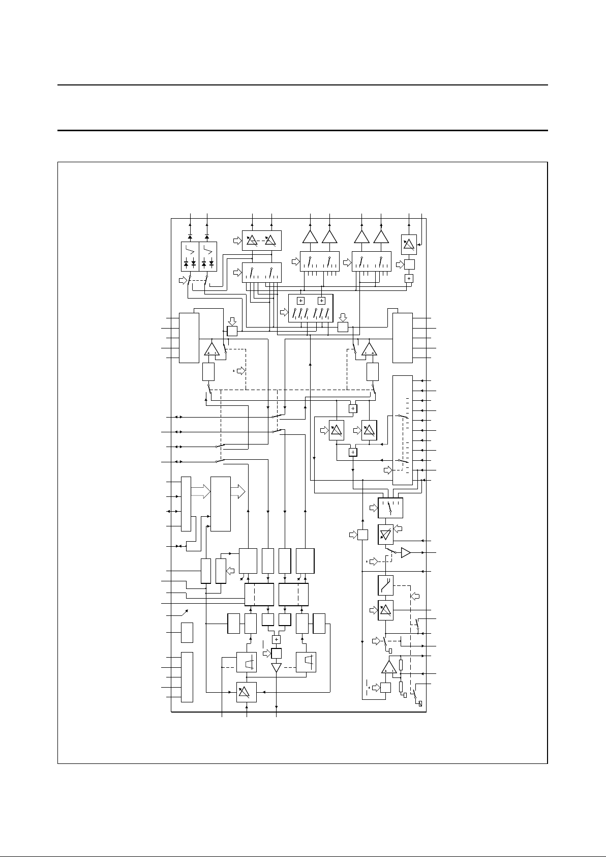
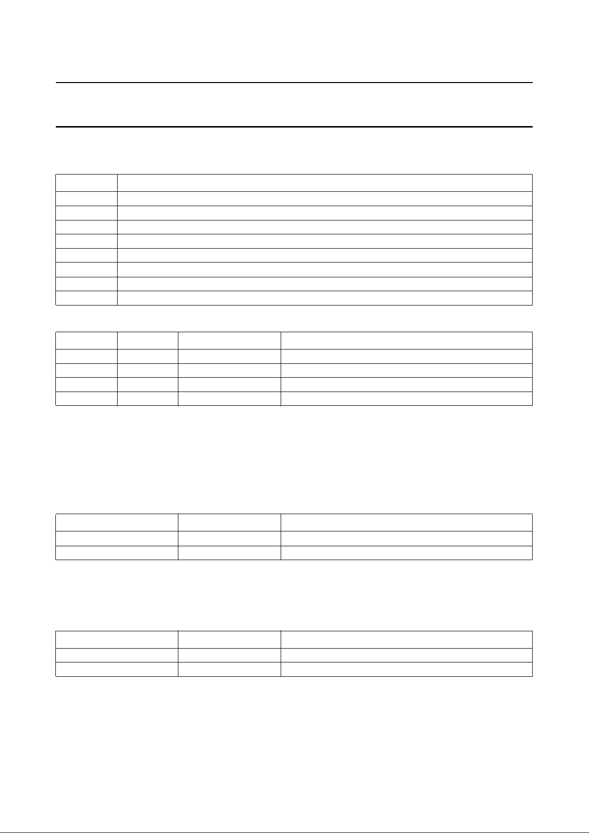
4 BLOCK DIAGRAM
MBE275
SUPPLY AND V
ref
I
ref
HF AGC
BPF
BPF
M
RAF
HF
LPF
HF
LIMITER
HF
LPF
LEVEL
DETECT
HF
LIMITER
LEVEL
DETECT
PLL
1.3 MHz
1.4 MHz
CCO
PLL
1.7 MHz
1.8 MHz
CCO
AUDIO
CLIPPER
SAMPLE-
AND-
HOLD
SAMPLE-
AND-
HOLD
AUDIO
CLIPPER
M
RN IPN RN
PBSet
PB eq
LP
RN IPN
AGCN
Normal Sel
Input Sel
NOISE REDUCTION
volume R
AUDIO
LPF
M
AFOMute
volume L
M
NOMute
Out Sel
M
RFCMute
volume HP
Line Sel
Dec Sel
HP Sel
2
6107113
8109
11
M
AFOMute
NOISE REDUCTION
AUDIO
LPF
DC Sel
RAF IPAF
DOC
DOC
MUTE
I C
2
50 43 58 54 42 49 61 53 59 60 62 12 13 14 15 16 63 64 52 51 37 38 39 40 41
23
24
25
26
19
20
21
22
18
17
48 47 46 45 447 8 9 10 112 3 4 5 61
28 29 2736353432333130
56
57
55
RBPF
FMIN
FMOUT
EQSW RECOUT PBIN
RECEQ LINREC RESSW
PBDC LININ
LINOUT
LINAGC SAP TUNR CINR EXT1R EXT2R EXT3R
TUNL CINL EXT1L EXT2L EXT3L
DCFBR EMPHR
DCREFR
DETR
RECTR
RFCAGC
RFCOUT
LINER
LINEL
LINE2R
LINE2L
HPOUTR
HPOUTL
DCOUTR
DCOUTL
DETL
RECTL
EMPHL
DCREFL
DCFBLAFNR
AFMR
AFNL
AFML
V
SSD
V
DDD SCLSDARAFCMUTE
ENVOUT
RCCOL
RCCOR
HIDRFIX
V
V
DDA1
V
SSA1
V
DDA2
V
SSA2
TDA9614H
ref
Fig.1 Block diagram.
Page 5
1995 Mar 21 5
Philips Semiconductors Preliminary specification
Audio processor for VHS hi-fi
and linear audio
TDA9614H
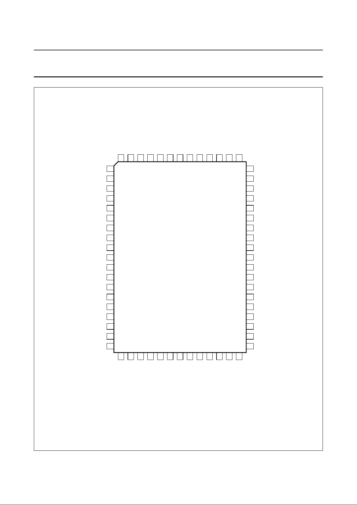
5 PINNING
SYMBOL PIN DESCRIPTION
SAP 1 Second Audio Program (SAP) input.
TUNL 2 Left channel tuner input.
TUNR 3 Right channel tuner input.
CINL 4 Left channel cinch input.
CINR 5 Right channel cinch input.
EXT1L 6 Left channel external 1 input.
EXT1R 7 Right channel external 1 input.
EXT2L 8 Left channel external 2 input.
EXT2R 9 Right channel external 2 input.
EXT3L 10 Left channel external 3 input.
EXT3R 11 Right channel external 3 input.
RAF 12 Record/playback switch drive output for head amplifier control or input for overruling
the I2C-bit RAF.
V
DDD
13 Digital supply voltage for I2C-bus (+5 V).
SDA 14 Data input/output for I2C-bus.
SCL 15 Clock input for I2C-bus.
V
SSD
16 Digital ground for I2C-bus.
RFCAGC 17 RF converter AGC-time constant.
RFCOUT 18 RF converter drive output.
LINE2L 19 Line 2 left output (e.g. decoder output).
LINE2R 20 Line 2 right output (e.g. decoder output).
LINEL 21 Line output left.
LINER 22 Line output right.
DCOUTL 23 VU meter drive output left.
DCOUTR 24 VU meter drive output right.
HPOUTL 25 Headphone drive output left.
HPOUTR 26 Headphone drive output right.
LINAGC 27 Linear audio AGC-time constant.
LININ 28 Audio input for linear audio to REC equalizer and output select.
LINOUT 29 Audio output from AGC or PB equalizer.
EQSW 30 Long Play (LP) equalization switch; 15 Ω on resistance and 150 kΩ input impedance.
RECEQ 31 Linear audio recording amplifier negative feedback input for connecting a record
equalization network.
LINREC 32 Digital output controlled by I2C-bit RN; can be used to drive an external (high voltage)
head switch and possibly the bias oscillator.
RECOUT 33 Linear audio recording amplifier output.
PBIN 34 Linear audio playback amplifier input; during playback the impedance is 100 kΩ;
during record the impedance is 7 Ω.
RESSW 35 Long Play equalization switch 50 Ω on and 150 kΩ off impedance to PBIN.
PBDC 36 Linear audio playback amplifier DC decoupling.
Page 6
1995 Mar 21 6
Philips Semiconductors Preliminary specification
Audio processor for VHS hi-fi
and linear audio
TDA9614H
DCFBL 37 DC feedback left.
DCREFL 38 DC reference left.
EMPHL 39 Total emphasis left (240 to 20 µs).
RECTL 40 Rectifier DC decoupling left.
DETL 41 Attack/recovery timing left.
V
ref
42 Noise filtering of 3.8 V reference voltage (external capacitor required for filtering).
V
SSA1
43 Analog ground 1 for LF circuits.
DETR 44 Attack/recovery timing right.
RECTR 45 Rectifier DC decoupling right.
EMPHR 46 Total emphasis right (240 to 20 µs).
DCREFR 47 DC reference right.
DCFBR 48 DC feedback right.
RFIX 49 Fixed bias current generation circuit by using an external 180 kΩ resistor to ground.
V
DDA1
50 Analog supply voltage 1 for LF circuits (+12 V).
AFNR 51 Audio output from noise reduction of right channel (record and loop-through) or audio
input for noise reduction of right channel (playback).
AFMR 52 Audio input for audio clipper of right channel (record and loop-through) or audio
output from sample-and-hold (playback).
RCCOR 53 Voltage-to-current transfer for right channel oscillator by means of an external resistor
to ground.
V
SSA2
54 Analog ground 2 for HF circuits.
RBPF 55 Bias current generation for the internal band-pass filters by means of an external
resistor to ground.
FMOUT 56 FM output.
FMIN 57 FM input.
V
DDA2
58 Analog supply voltage 2 for HF circuits (+5 V).
RCCOL 59 Voltage-to-current transfer for left channel oscillator by means of an external resistor
to ground.
ENVOUT 60 Level detector output (external capacitor required for filtering).
HID 61 Head Identification Pulse (HID) input for sample-and-hold circuits.
CMUTE 62 Mute timing (external capacitor required for playback mute).
AFML 63 Audio input for audio clipper of left channel (record and loop-through) or audio output
from sample-and-hold circuit of left channel (playback).
AFNL 64 Audio output from noise reduction of left channel (record and loop-through) or audio
input for noise reduction of left channel (playback).
SYMBOL PIN DESCRIPTION
Page 7
1995 Mar 21 7
Philips Semiconductors Preliminary specification
Audio processor for VHS hi-fi
and linear audio
TDA9614H
Fig.2 Pin configuration.
handbook, full pagewidth
TDA9614H
MBE278
1
2
3
4
5
6
7
8
9
10
11
12
13
14
15
16
17
18
19
51
50
49
48
47
46
45
44
43
42
41
40
39
38
37
36
35
34
33
20
21
22
23
24
25
26
27
28
29
30
31
32
64
63
62
61
60
59
58
57
56
55
54
53
52
RECOUT
PBIN
RESSW
PBDC
DCFBL
DCREFL
EMPHL
RECTL
DETL
V
DETR
RECTR
EMPHR
DCREFR
DCFBR
RFIX
AFNR
ref
V
SSA1
V
DDA1
SAP
TUNL
TUNR
CINL
CINR
EXT1L
EXT1R
EXT2L
EXT2R
EXT3L
EXT3R
RAF
V
SDA
SCL
RFCAGC
RFCOUT
LINE2L
LINE2R
LINEL
LINER
DCOUTL
DCOUTR
HPOUTL
HPOUTR
LINAGC
LININ
LINOUT
EQSW
RECEQ
LINREC
DDD
V
SSD
AFNL
AFML
CMUTE
HID
ENVOUT
RCCOLVFMIN
FMOUT
RBPF
RCCOR
AFMR
DDA2
V
SSA2
Page 8

1995 Mar 21 8
Philips Semiconductors Preliminary specification
Audio processor for VHS hi-fi
and linear audio
TDA9614H
6 FUNCTIONAL DESCRIPTION
MBE276
TDA9614H
InputSel
TUNER
CINCH
EXT1
EXT2
EXT3
SAP
NORMAL
EXT3/ST
Volume L/R
14 dBto49 dB
MUTE
AFM MUTE
AFOMute
OutSel
STEREO
LEFT
RIGHT
NORMAL
NOR ST
NOR L
NOR R
MUTE
NORMAL MUTE
NOMute
AGC
ON
OFF
NormalSel
InputSel
InputSel Volume
SAP
TUNER-left
HPSel
OutSel
LEFT
RIGHT
NORMAL
TUNER
CINCH
EXT1
EXT2
EXT3
SAP
LineSel
OutSel
NORMAL
EXT2
EXT3
Volume HP
16 dBto47 dB
MUTE
Decoder Sel
OutSel
TUNER
EXT1
EXT3
MUTE
RFCmute
DCSel
HPSel
STEREO
RFC
LINE
LINE2
decoder
headphone
VU meter
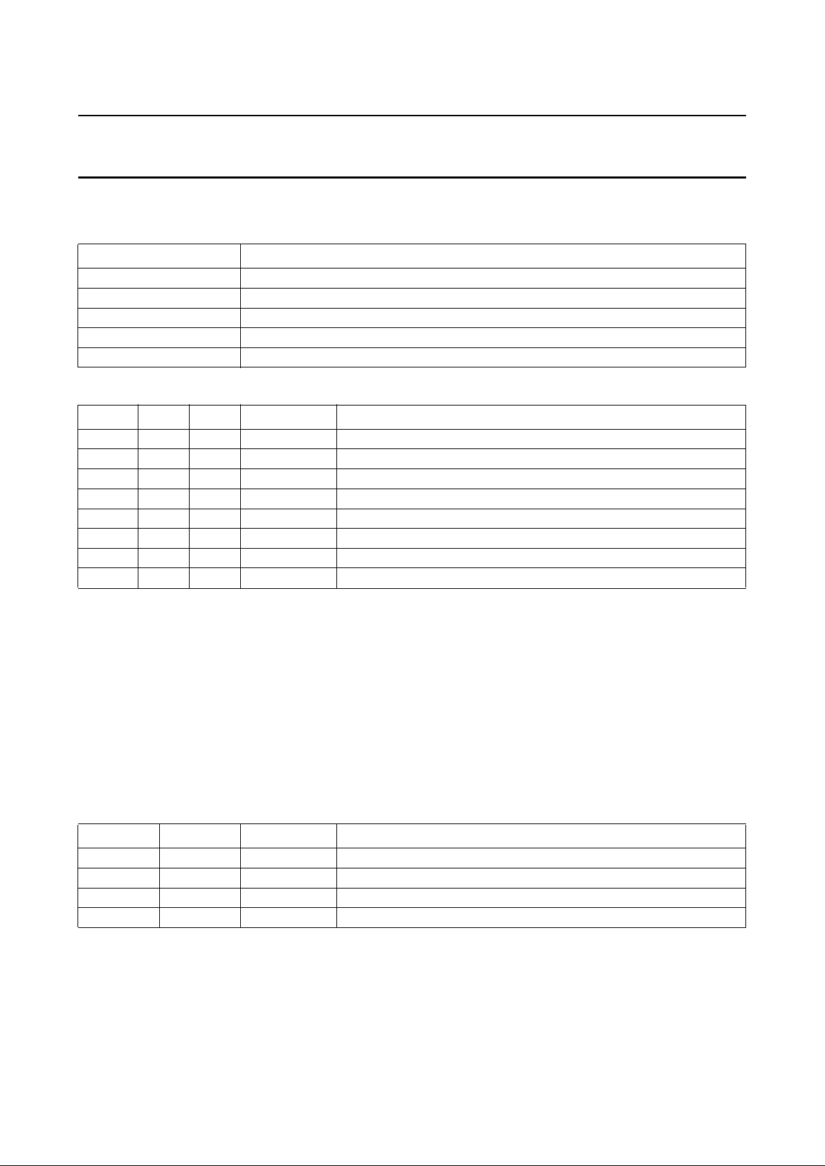
Fig.3 Audio input/output selections.
Page 9

1995 Mar 21 9
Philips Semiconductors Preliminary specification
Audio processor for VHS hi-fi
and linear audio
TDA9614H
6.1 Audio I/O switching
6.1.1 INPUT SELECT (INPUTSEL)
For the audio FM circuitry eight different audio signals can
be selected. The selection made here for hi-fi is also
available for the linear audio circuitry.
1. TUNER (stereo input; internal tuner of VCR).
2. CINCH (stereo input; connection to hi-fi set).
3. EXT1 (stereo input; TV SCART1).
4. EXT2 (stereo input; decoder, 2nd VCR SCART2).
5. EXT3 (stereo input; front CINCH for e.g. camcorder).
6. SAP (mono input; ‘Second Audio Program’ audio
carrier for NTSC or conventional FM carrier with
NICAM reception).
7. NORMAL (linear audio; [playback] signal of linear
audio).
When inserting a new video signal in an old
audio/video recording the hi-fi audio track is erased.
This setting can keep the current audio available on
the hi-fi track by copying the (playback) linear audio
signal to the hi-fi track during video insert.
8. EXT3/ST (input mix; mono EXT3 on left, mono hi-fi on
right channel).
For linear audio use see Section 6.1.2.
6.1.2 NORMAL SELECT (NORMSEL)
For linear audio four settings can be selected:
1. INPUTSEL (mono signal from input select).
This is the ‘standard’ setting. The signal source
selected with the input select is led to the linear audio
circuit. The linear audio AGC should be switched on.
2. VOLUME (mono signal from [hi-fi] volume control).
The signal source selected with the input select has
now volume control, the linear audio AGC should be
switched off. This setting is for use with ‘audio
dubbing’: inserting a new audio signal on the linear
track in an old audio/video recording. A special audio
dubbing feature is now possible by selecting ‘input mix’
EXT3/ST in the input select. This setting enables us to
use the VCR as a mixer console: an audio source
connected to EXT3 (front CINCH) can be adjusted and
mixed together with the original hi-fi playback signal,
using the left (EXT3) and right (hi-fi playback) volume
controls.
3. SAP (SAP input).
This setting enables simultaneous recording of the
NTSC SAP signal on the linear track and TUNER
stereo on the audio FM track. When receiving a
NICAM audio signal, the linear audio can be used as a
‘backup’ track when received television signals are
weak.
4. TUNER LEFT (left channel [language 1] of TUNER
input).
When receiving dual language transmissions the main
language (language 1) can be recorded on linear
audio. Note that if the SAP input is not used it can be
connected to the right TUNER channel, enabling
language selection for linear audio.
6.1.3 VOLUME L/R; AGC
The volume controls are mainly intended for level
adjusting of the audio signals to be recorded on the hi-fi
track, however using the ‘VOLUME’ setting in the Normal
Select it can also be used to control linear audio. The
volume controls have a control range of +14 dB to −49 dB
in 1 dB steps and a full mute. Because the volume controls
are I2C-bus controlled their actual behaviour is defined by
the VCR’s software. For instance user control can be
‘volume only’, ‘left + right’, ‘volume + balance’ or the
setting can be defined by a ‘digital AGC’ software loop
using the signals at the DC (VU meter) outputs.
The linear audio level can be controlled by an AGC circuit,
which can be switched off when desired. In most cases the
AGC should be used at all settings of the Normal Select
except for ‘VOLUME’.
6.1.4 AUDIO FM OUTPUT MUTE (AFOMUTE);
NORMAL OUTPUT MUTE (NOMUTE)
The audio output signal of the audio FM circuit can be
muted with AFOMute, the linear output signal can be
muted using NOMute. If one of these signals is not used
as an output (or input) signal it is best muted to further
minimize crosstalk.
6.1.5 OUTPUT SELECT (OUTSEL)
This block is the ‘main’ output select function, possibly
functional on all outputs. Each output however has some
means to override this selection for its own output signal,
to implement extra features. Eight selections are possible
and they are shown in Table 1.
Page 10
1995 Mar 21 10
Philips Semiconductors Preliminary specification
Audio processor for VHS hi-fi
and linear audio
TDA9614H
Table 1 Output select possibilities
Note
1. STEREO is the ‘standard’ setting, LEFT and RIGHT are for language selection. Using the tuner as input or output
signal (record or loop-through of audio FM) the VCR can automatically switch from stereo to left (language 1) when
a ‘dual language’ transmission is received. If the VCR is in playback mode and no hi-fi track is present (checking bit
AFOM via the I2C-bus or using the level at pin 11) the VCR can switch the output select to NORMAL (or let the IC
do this automatically by setting bit AUTN). If a hi-fi track is present the user may want to switch to LEFT and RIGHT
if the recording made was a ‘dual language’ recording.
Furthermore the user may want to switch from a hi-fi selection to NORMAL, e.g. when a complete audio remix has
been created on the linear track using ‘audio dubbing’ (see Section 6.7). ‘Audio dubbing’ can also be used to
re-record the linear track with e.g. only commentary. Combined playback of this commentary together with the
original hi-fi sound is then possible by means of a mix mode.
6.1.6 RF CONVERTER MUTE (RFCMUTE)
The RFC output is a mono output derived from the output select, its output signal can be muted.
6.1.7 LINE SELECT (LINESEL)
The line output select is normally connected to both CINCH (hi-fi set) and television (SCART1). Normally the audio signal
from the output select will be available at this output, but three extra selections are possible and they are shown in
Table 2.
Table 2 Extra line select possibilities
Notes
1. A signal from a source at EXT2 (laser disc or second VCR) can be connected to a television set at line out. Because
this is a direct connection from the input to the line output buffers it is fully independent of any mode setting of the
IC. Connection of a ‘Pay-TV’ decoder box to EXT2 and using this selection together with selecting EXT1 in the
decoder select enables combined use of the decoder box by both TV and VCR. In Europe, use of the SCART
connector ‘status line’ can automatize this switching.
2. Direct audio connection from input EXT3. If the line 2 outputs and EXT3 inputs are not used for external connections
a built-in karaoke unit or sound processor can be inserted between line 2 and EXT3.
SELECTION REMARK DESCRIPTION
STEREO
(1)
hi-fi stereo audio FM output signal left and right channel
LEFT hi-fi left audio FM output signal left channel (language 1)
RIGHT hi-fi right audio FM output signal right channel (language 2)
NORMAL linear audio linear audio
NOR + ST linear and hi-fi mix of audio FM stereo and linear audio
NOR + L linear and left mix of audio FM left channel and linear audio
NOR + R linear and right mix of audio FM right channel and linear audio
MUTE mute
SELECTION DESCRIPTION
NORMAL linear audio, useful for monitoring during ‘audio dubbing’
EXT2
(1)
audio from input EXT2
EXT3
(2)
audio from input EXT3
Page 11
1995 Mar 21 11
Philips Semiconductors Preliminary specification
Audio processor for VHS hi-fi
and linear audio
TDA9614H
6.1.8 DECODER SELECT (DECODESEL)
The line 2 output is normally connected to a decoder box
or e.g. a second VCR (SCART2). Normally the audio
signal from the output select will be available at this output,
but three extra selections are shown in Table 3.
Table 3 Extra decoder select possibilities
Notes
1. Enables the use of a decoder box (connected to line 2
[EXT2]) by the VCR.
2. Decoder box connection to television set
(See Section 6.1.7).
6.1.9 HEADPHONE SELECT (HPSEL)
The headphone output will normally carry the output select
signal, however three more selections are possible and
shown in Table 4.
Table 4 Extra headphone select possibilities
Note
1. The selections LEFT and RIGHT make it possible to
select a different language for the headphone as for
the line outputs. A possible implementation is to invert
always a language selection made at the output select.
6.1.10 H
EADPHONE VOLUME
The headphone volume control has a control range of
+16 dB to −47 dB in 1 dB steps and a full mute.
6.1.11 DC SELECT (DCSEL)
The VU meter output is normally connected to the
headphone select, but can also be switched to STEREO
(hi-fi stereo, before the output select). When using the
VU meter output signal to implement a ‘digital AGC’ (read
the level at the DC output, and adjust the VOLUME L/R
controls accordingly) it is necessary to have information of
SELECTION DESCRIPTION
TUNER
(1)
audio from input TUNER
EXT1
(2)
audio from input EXT1
EXT3 audio from input EXT3
SELECTION DESCRIPTION
LEFT
(1)
left hi-fi channel
RIGHT
(1)
right hi-fi channel
NORMAL linear audio, useful for monitoring the
recording by ‘audio dubbing’
both hi-fi audio channels, independent from the setting of
output or headphone select. For this mode the selection
STEREO can be made.
6.2 Linear audio circuits
6.2.1 RECORD/LOOP-THROUGH
The signal selected with the normal select can be level
controlled in the AGC block. If wanted this AGC can be
switched off using bit AGCN. The audio signal is thereafter
DC decoupled using a capacitor between pin 29 (LINOUT)
and pin 28 (LININ).
From here on the signal goes to the output select and (in
the event of record mode) to the record equalizer. The
record equalizer is a non-inverting amplifier with a gain of
+12 dB, consisting of an opamp with feedback resistors,
and acts as a pre-correction filter for the tape and head
characteristics. The inverting input of the opamp is
connected to pin 31 (RECEQ), its output to pin 33
(RECOUT). The circuit externally connected between
pin 31 and ground defines the transfer of the record
equalizer with equation:
Where: Z is the complex impedance of the external circuit.
Two equalizings can be used, switching additional circuitry
to ground with pin 30 (EQSW) in long play or extended
play (I2C-bus: LP = 1).
Instead of the hi-fi circuit, linear audio has two
loop-through modes:
• Loop-through playback
• Loop-through record.
The only difference between Loop-through record and
record is the RECOUT output, which is muted.
The LINREC output (pin 32) is used to drive the external
high-voltage switch and possibly the bias oscillator. The
LINREC voltage has a small internal delay to be
non-overlapping with the internal switching to playback
mode. This ensures that no bias voltage will appear at the
PBIN input while the IC is in playback mode.
6.2.2 P
LAYBACK
The signal coming from the head is amplified and can be
level controlled in 16 steps of 1 dB. This setting can be
used to adjust for spread or nominal difference in head
output level. Afterwards, the signal is frequency corrected
in the playback equalizer. This equalizer includes the two
standard VHS equalizing settings of 3180 and 120 µs
A 3.98
1200 Z
+( )
Z
------------------------------
×=
Page 12

1995 Mar 21 12
Philips Semiconductors Preliminary specification
Audio processor for VHS hi-fi
and linear audio
TDA9614H
(standard play: LP = 0) and 3180 and 170 µs (Long Play:
LP = 1).
The signal is DC decoupled and routed to the output select
via pins 29 and 28. When switching to or from playback
the signal should be muted shortly using the Normal
Output Mute (NOM) to prevent audible clicks caused by
offset differences of the playback amplifier and AGC.
6.3 Audio FM circuits
6.3.1 RECORD/LOOP-THROUGH
After low-pass filtering and signal compression in the
Noise Reduction (NR) the audio signal is available at
AFNL and AFNR. Through a DC-decoupling capacitor the
compressed audio signal is fed to an audio clipper at
AFML and AFMR. Subsequently, the audio signal is
FM-modulated on a RF-carrier using an integrated
current-controlled oscillator (CCO). Each CCO (L and R)
requires an external resistor (RCCOL/R) for temperature
stability. Through automatic calibration both the oscillator
centre frequency and FM-deviation are adjusted. After
low-pass filtering and summation of the two RF-carriers,
the FM signal is available at FMOUT during record. During
loop-through the FMOUT pin is inactive.
The RAF pin reflects the status of the RAF-bit when it is
used as output pin. In this case it is meant to switch the
head amplifier between record and playback position. It
can also be used as an input pin to overrule the RAF-bit
thereby forcing the IC in record or playback/loop-through
position.
6.3.2 PLAYBACK
The two FM modulated RF carriers, presented at FMIN,
are fed to an AGC circuit. The AGC operates on the peak
level of the added BPF output signals. As a result, the input
signal of the BPFs is kept constant for FMIN voltages
>30 mV (RMS value) both carriers added. In this way the
dynamic range of the integrated BPFs is optimally used
over a large input signal range. Subsequently, the
RF carriers are bandpass filtered using two integrated
BPFs. These bandpass filters are automatically calibrated
as described in Section 6.3.3. An external resistor (RBPF)
is required for temperature stability.
The filtered input signals are fed to a limiter. The limiter
output signal is demodulated by means of a
PLL demodulator. The LF audio signal is fed through a
sample-and-hold circuit to suppress head-switching noise.
The demodulated audio is available at AFML and AFMR.
Through a decoupling capacitor the audio signal is applied
to an audio low-pass filter at AFNL and AFNR. The
low-pass filtered audio signal is expanded in the noise
reduction.
If the left channel carrier at FMIN falls below the mute level
of 4.2 mV (RMS value) the audio signal is muted in front of
the low-pass filter. This is achieved by comparing the left
channel level detector signal with an internal reference.
The mute timing is fixed by a capacitor at the CMUTE pin.
If the level at CMUTE rises above a certain threshold, the
PBMUTE bit is set. This will mute the audio signal. If bit
AUTN has been set, the output selection will automatically
switch to NORMAL mode. The left channel level detector
output is also available at pin ENVOUT. An AGC
correction voltage is added at this pin, such that the
ENVOUT voltage indicates the left channel FM-carrier
level even within the AGC-range. The ENVOUT voltage
can be used for auto-tracking of the FM-audio heads.
In the event of drop-outs in the incoming FM signal, the left
channel level detector is also used to activate the
sample-and-hold. This drop-out cancellation is only active
if bit DOC has been set.
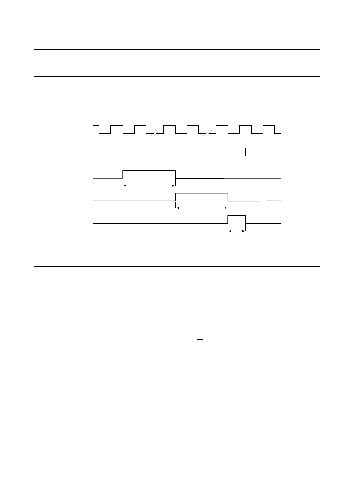
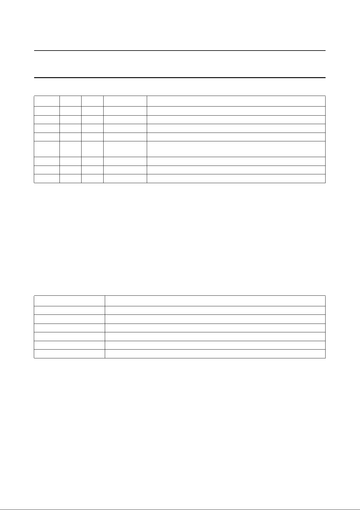
6.3.3 AUTOMATIC CALIBRATION
By means of bit CALS the two integrated oscillators and
bandpass filters can be calibrated in Loop-Through (LT) or
record (REC) mode. Normally this will be done after
start-up of the VCR. After setting of bit CALS the
calibration procedure is automatically executed as shown
in Fig.4. The calibration starts at the first negative edge of
HID after CALS has been set. During the LOW period of
HID (20 ms for PAL) the number of oscillator cycles is
compared to a certain value stored in a Read Only Memory
(ROM).
Therefore, the final oscillator frequency is proportional to
the inverse of the HID LOW-time. This means that an error
of 1 µs in the HID LOW-time will result in an additional
frequency error of approximately 100 Hz. The maximum
number of required HID cycles for one complete oscillator
calibration is six, which is equal to 240 ms.
After both oscillators have been calibrated the bandpass
filters are calibrated using the right channel oscillator as
reference frequency generator (1.6 MHz for PAL). This will
take <10 ms.
Bit CALR is set to 1 if the calibration has been executed
successfully. CALR is 0 if:
• A Power-On Reset (POR) has occurred.
• The calibration is running.
• The initial oscillator and bandpass frequencies are too
low or too high for a successful calibration.
Page 13
1995 Mar 21 13
Philips Semiconductors Preliminary specification
Audio processor for VHS hi-fi
and linear audio
TDA9614H
Fig.4 Timing diagram of automatic calibration.
MBE281
max 240 ms
max 240 ms
max 10 ms
HID
CALS
LEFT
OSCILLATOR
RIGHT
OSCILLATOR
CALR
BANDPASS
FILTERS
If CALS is reset during CALR = 0, the calibration will be
stopped if it was not finished yet. If required, a new
calibration can be started using CALS.
WARNING: the IC should not be calibrated in a test or
standby mode.
6.3.4 PAL/NTSC MODE
Depending on bit NTSC the IC is calibrated in PAL or
NTSC mode using bit CALS. After an automatic calibration
the oscillator frequencies can be switched between PAL
and NTSC using bit NTSC. This centre frequency shift is
done without automatic calibration. During playback (PB)
or loop-through (LT) a change in bit NTSC will
automatically calibrate the bandpass filters again. This will
take <10 ms.
WARNING: A change of PB to REC, LT to REC and
PAL to NTSC should not be combined in one transmitted
byte. The PAL to NTSC transition should be preceded by
the PB to REC or LT to REC transition.
6.4 I2C-bus
The TDA9614H is controlled via the 2-wire I2C-bus, in
accordance with the I2C-bus specification. As slave
receiver for programming there is one module address,
with R/
W bit = 0, a subaddress byte and eight data bytes.
If more than one data byte follows the subaddress, these
bytes are stored in the successive registers by the
automatic address increment feature. As slave transmitter
(R/W bit = 1) there is one read byte.
Page 14
1995 Mar 21 14
Philips Semiconductors Preliminary specification
Audio processor for VHS hi-fi
and linear audio
TDA9614H
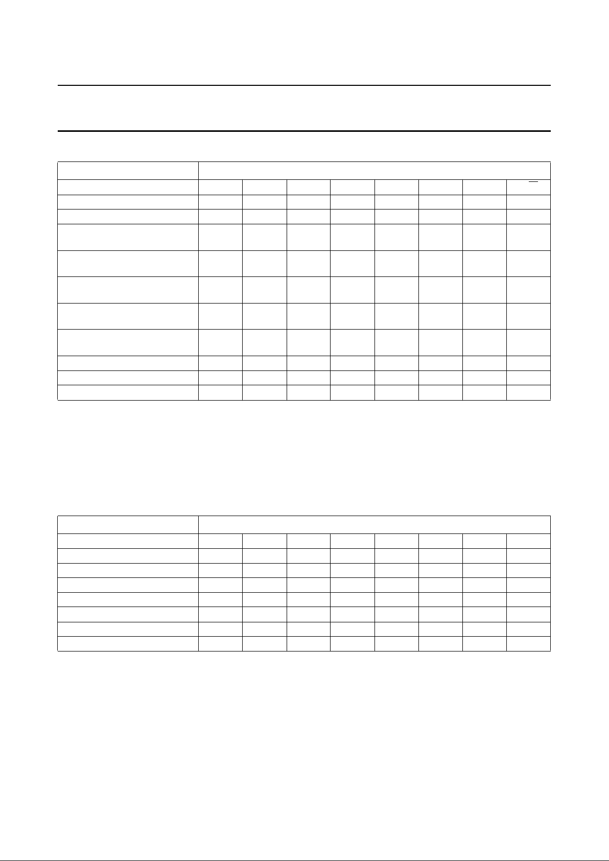
Table 5 TDA9614H addresses and data bytes
Note
1. These bits determine the subaddress.
6.5 Power-On Reset (POR); derived from digital supply voltage V
DDD
In the data byte descriptions [por] indicates the mode after POR. The status of the data bytes after POR is shown in
Table 6.
Table 6 Status of data bytes after POR
A POR occurrence is signalled by bit POR in the read byte (see Table 39).
NAME ADDRESS
Slave address byte 1 0 1 1 1 0 0 R/
W
Subaddress bytes 00 to 07 0 0 0 0 0 X
(1)
X
(1)
X
(1)
Control byte (subaddress 00) RAF IPAF AFOM NTSC RN IPN NOM LP
Main select byte
(subaddress 01)
IS2 IS1 IS0 NS1 NS0 OSL OSR OSN
Secondary select byte
(subaddress 02)
HSL HSR DCS RFCM LOS1 LOS0 DOS1 DOS0
Left volume byte
(subaddress 03)
0 VLM VL5 VL4 VL3 VL2 VL1 VL0
Right volume byte
(subaddress 04)
0 VRM VR5 VR4 VR3 VR2 VR1 VR0
Headphone volume byte
(subaddress 05)
0 VHM VH5 VH4 VH3 VH2 VH1 VH0
Install byte (subaddress 06) DEV1 DEV0 NPL3 NPL2 NPL1 NPL0 AUTN DOC
Test byte (subaddress 07) STBY CALS AGCN TST4 TST3 TST2 TST1 TST0
Read byte (address B9) CALR PAFM 1 POR 1 0 1 1
DATA BYTE ADDRESS
Control byte 0 1 1 0 0 1 1 0
Main select byte 0 0 0 0 0 1 1 0
Secondary select byte 1 1 0 0 0 0 0 0
Left volume byte 0 0 1 1 0 0 0 1
Right volume byte 0 0 1 1 0 0 0 1
Headphone volume byte 0 0 1 0 1 1 1 1
Install byte 0 1 0 1 1 1 0 1
Test byte 0 0 0 0 0 0 0 0
Page 15
1995 Mar 21 15
Philips Semiconductors Preliminary specification
Audio processor for VHS hi-fi
and linear audio
TDA9614H
6.6 Control byte
Table 7 Bits of control byte
Table 8 Bits RAF and IPAF
Notes
1. The RAF bit can be overruled externally by applying a low-ohmic voltage to the RAF I/O (pin 12) either logic 0 or
logic 1 (0 or +5 V). The actual mode of the IC is determined by the level measured at this pin, enabling fast switching
between record and playback/loop-through.
2. The two record modes are equal, only differing in their reaction to forcing RAF LOW at the RAF I/O pin; the status of
the IPAF bit determines whether the IC is switched to the playback or loop-through mode.
Table 9 Bit AFOM
Note
1. Audio coming from the audio FM circuit is muted, either the signal from tape in playback or the loop-through signal
in record or loop-through modes.
Table 10 Bit NTSC
BIT DESCRIPTION
RAF Record Audio FM; see Table 8
IPAF Inverse Playback Audio FM; see Table 8
AFOM Audio FM Output Mute; see Table 9
NTSC NTSC; television standard; see Table 10
RN Record Normal; see Table 11
IPN Inverse Playback Normal; see Table 11
NOM Normal Output Mute; see Table 12
LP Long Play mode; see Table 13
RAF
(1)
IPAF MODE DESCRIPTION
0 0 playback NR and modem in playback mode
0 1 loop-through NR in record mode; modem not active [por]
1 0 record
(2)
NR and modem in record mode
1 1 record
(2)
NR and modem in record mode
AFOM MODE DESCRIPTION
0 − −
1 mute
(1)
output from audio FM (NR) circuit is muted [por]
NTSC MODE DESCRIPTION
0 PAL modem and BPF set to PAL carrier frequencies [por]
1 NTSC modem and BPF set to NTSC carrier frequencies
Page 16

1995 Mar 21 16
Philips Semiconductors Preliminary specification
Audio processor for VHS hi-fi
and linear audio
TDA9614H
Table 11 Bits RN and IPN
Notes
1. Bit RN is output at LINREC (pin 32), which is used to drive an external (high voltage) head switch and possibly the
bias oscillator. The two loop-through modes are equal in signal flow, however they differ in the state of the head
switches (the internal switch at PBIN [pin 34] and the external head switch driven by pin LINREC).
2. Loop-through R is equal to record except for the RECOUT output (pin 33) which is muted.
Table 12 Bit NOM
Note
1. Audio coming from the linear audio circuit is muted, either the signal from tape in playback or the loop-through signal
in record or loop-through modes. To avoid clicks when changing the mode of the linear audio circuit to or from
playback, the output should be muted shortly, using this bit.
Table 13 Bit LP
RN
(1)
IPN MODE DESCRIPTION
0 0 playback linear audio circuit in playback mode
0 1 loop-through P linear audio circuit in loop-through mode (playback ready) [por]
1 0 loop-through R
(2)
linear audio circuit in loop-through mode (record ready)
1 1 record linear audio circuit in record mode
NOM MODE DESCRIPTION
0 − −
1 mute
(1)
output from linear audio circuit is muted [por]
LP MODE DESCRIPTION
0 SP Record and playback equalizing set for Standard Play [por].
Record equalization switch at EQSW (pin 30) and playback equalization switch at RESSW
(pin 35) are open (high impedance). The internal playback equalizing is 3180 and 120 µs.
It can be changed to 2544 and 96 µs by selecting test number 31 (see Section 6.12).
1 LP Record and playback equalizing set for Long Play.
Record equalization switch at EQSW (pin 30) and playback equalization switch at RESSW
(pin 35) are closed. The internal playback equalizing is 3180 and 170 µs. It can be
changed to 2731 and 146 µs by selecting test number 31 (see Section 6.12).
Page 17
1995 Mar 21 17
Philips Semiconductors Preliminary specification
Audio processor for VHS hi-fi
and linear audio
TDA9614H
6.7 Main select byte
Table 14 Bits of main select byte
Table 15 Bits IS2 to IS0; note 1
Notes
1. With bits IS2 to IS0, the stereo input signal is selected which is led to the hi-fi processing. One out of five stereo
sources can be selected. The five stereo inputs differ in their connectivity; with bits NS1 and NS0 tuner left
(TUNL; pin 2) can be selected as linear audio input source, with bits LOS1 and LOS0 Normal, Ext2 and Ext3 are
directly connectable to Line out and to DOS1 and DOS0 Tuner, Ext1 and Ext3 are directly connectable to decoder
out (2nd Line Out).
2. Remark: when using the selections Normal or Dub Mix be aware of signal loops (which should be avoided) because
this can lead to large audio oscillations.
3. The selection Dub Mix is a special function in which a mono signal derived from the Ext3 inputs
(1⁄2EXT3L +1⁄2EXT3R) is led to the left input and a mono signal derived from the audio FM output (1⁄2L +1⁄2R) is led
to the right input channel. This function can be used for audio dubbing using the volume controls as a mixing desk.
Table 16 Bits NS1 and NS0; note 1
Note
1. With bits NS1 and NS0 the input signal is selected for the linear audio circuit. When a stereo input source is selected,
a mono signal is made by adding the left and right channel. Furthermore two independent selections can be made
(the mono input SAP or the left channel of tuner e.g. for dual language). If in the volume mode the built-in AGC circuit
is switched off by using bit AGCN, the audio level can be controlled by the left and right volume controls
(VLx and VRx).
BIT DESCRIPTION
IS2 to IS0 Input Select 2 to Input Select 0; see Table 15
NS1 and NS0 Normal Select 1 and Normal Select 0; see Table 16
OSL Output Select Left; see Table 17
OSR Output Select Right; see Table 17
OSN Output Select Normal; see Table 17
IS2 IS1 IS0 MODE SELECTED INPUT SOURCE
0 0 0 Tuner TUNL and TUNR [por]
0 0 1 Cinch CINL and CINR
0 1 0 Ext1 EXT1L and EXT1R (e.g. SCART1; TV connector)
0 1 1 Ext2 EXT2L and EXT2R (e.g. SCART2; decoder connector)
1 0 0 Ext3 EXT3L and EXT3R (e.g. front cinch)
1 0 1 SAP additional mono input (SAP; pin 1)
1 1 0 Normal
(2)
output from linear audio (LININ; pin 28)
1 1 1 Dub Mix
(2)(3)
mixing of EXT3 input with hi-fi output signal
NS1 NS0 MODE DESCRIPTION
0 0 Input linear audio input source is equal to hi-fi input [por]
0 1 Volume linear audio input source is equal to hi-fi input, inclusive volume control
1 0 SAP additional mono input (SAP; pin 1) is selected
1 1 Tuner L left channel of tuner input is selected
Page 18
1995 Mar 21 18
Philips Semiconductors Preliminary specification
Audio processor for VHS hi-fi
and linear audio
TDA9614H
Table 17 Bits OSL, OSR and OSN; note 1
Note
1. The bits OSL, OSR and OSN provide eight output select functions. LEFT and RIGHT are the left and right hi-fi
channels; NORMAL is the linear audio channel (LININ; pin 28). This selection is normally output at line out (LINEL
and LINER), RFCOUT (pin 18), decoder out (LINE2L and LINE2R), headphone out (HPOUTL and HPOUTR) and
DC out (DCOUTL and DCOUTR). However line out can be overruled by bits LOS1 and LOS0; decoder out can be
overruled by bits DOS1 and DOS0, headphone out (and DC out) can be overruled by bits HSL and HSR and DC out
can be overruled by bit DCS.
Remark: if AUTN = 1 (see Section 6.11) the output select modes stereo, left and right will be forced to normal as long
as the audio FM circuit is in playback mode and the internal PB mute signal is generated (no hi-fi track on tape). The
status of this internal mute signal can be read by bit PAFM (see Section 6.13).
6.8 Secondary select byte
Table 18 Bits of secondary select byte
OSL OSR OSN MODE DESCRIPTION
1 1 0 stereo LEFT at left channel; RIGHT at right channel [por].
1 0 0 left LEFT at both left and right channels.
0 1 0 right RIGHT at both left and right channels.
0 0 0 mute No selection.
1 1 1 mixed stereo LEFT + NORMAL added at left channel; RIGHT + NORMAL added at
right channel.
1 0 1 mixed left LEFT + NORMAL added at both left and right channels.
0 1 1 mixed right RIGHT + NORMAL added at both left and right channels.
0 0 1 normal NORMAL (is linear audio) at both left and right channels.
BIT DESCRIPTION
HSL Headphone Select Left; see Table 19
HSR Headphone Select Right; see Table 19
DCS DC Select; see Table 20
RFCM RFC Mute; see Table 21
LOS1 and LOS0 Line Output Select 1 and Line Output Select 0; see Table 22
DOS1 and DOS0 Decoder Output Select 1 and Decoder Output Select 0; see Table 23
Page 19

1995 Mar 21 19
Philips Semiconductors Preliminary specification
Audio processor for VHS hi-fi
and linear audio
TDA9614H
Table 19 Bits HSL and HSR
Normally the headphone output signal is set by the output selection OSL, OSR and OSN (see Table 17). Furthermore
three independent selections can be made: LEFT hi-fi channel, RIGHT hi-fi channel (language selection) and NORMAL
(e.g. monitoring an audio dubbing recording). These headphone selections are also active for the VU meter output
(DC out), unless bit DCS = 1.
Table 20 Bit DCS
Note
1. The signal at DC out (DCOUTL and DCOUTR; pins 23 and 24) is normally the signal which can be listened to by the
headphone. For use in concepts with digital AGC (using the DC output signal to control the left and right volume
settings), an independent selection to hi-fi stereo can be made.
Table 21 Bit RFCM
Note
1. The audio signal at RF converter out (a mono version of the signal selected with the output select with overload AGC)
can be independently muted.
Table 22 Bits LOS1 and LOS0; note 1
Note
1. With the line output select some special connections can be made overruling the output select (OSL, OSR and OSN),
e.g. for connecting a decoder box (for a pay-TV channel) to a television set via the VCR.
HSL HSR MODE DESCRIPTION
1 1 outsel Headphone signal set by the output selection [por].
1 0 left LEFT at both headphone out left and right.
0 1 right RIGHT at both headphone out left and right.
0 0 normal NORMAL (is linear audio) at both headphone outputs.
DCS MODE DESCRIPTION
(1)
0 headphone DC output is set by Headphone Select [por].
1 stereo DC output is hi-fi stereo.
RFCM MODE DESCRIPTION
(1)
0 − [por]
1 mute
(1)
RF converter output signal muted
LOS1 LOS0 MODE DESCRIPTION
0 0 Outsel Line output selection is set by output select function [por].
0 1 Normal Linear audio is connected to line output.
1 0 Ext2 Ext2 input is directly connected to line output.
1 1 Ext3 Ext3 input is directly connected to line output.
Page 20

1995 Mar 21 20
Philips Semiconductors Preliminary specification
Audio processor for VHS hi-fi
and linear audio
TDA9614H
Table 23 Bits DOS1 and DOS0; note 1
Note
1. With the decoder output select some special connections can be made overruling the output select (OSL, OSR and
OSN), e.g. for connecting a decoder box to the VCR.
6.9 Left/Right (L/R) volume byte
Table 24 Bits of Left/Right volume byte
Table 25 Left/Right volume byte; notes 1 and 2
DOS1 DOS0 MODE DESCRIPTION
0 0 Outsel Decoder output selection is set by output select function [por].
0 1 Tuner Tuner input is directly connected to decoder output.
1 0 Ext1 Ext1 input is directly connected to decoder output.
1 1 Ext3 Ext3 is directly connected to decoder output.
BIT DESCRIPTION
VLM Volume Left Mute; see Table 25
VL5 to VL0 Volume Left 5 to Volume Left 0; see Table 25
VRM Volume Right Mute; see Table 25
VR5 to VR0 Volume Right 5 to Volume Right 0; see Table 25
VLM VL5 VL4 VL3 VL2 VL1 VL0
MODE
VRM VR5 VR4 VR3 VR2 VR1 VR0
1 X X X X X X mute
0 0 0 0 0 0 0 −49 dB
0 0 0 0 0 0 1 −48 dB
0 0 0 0 0 1 0 −47 dB
0 0 0 0 0 1 1 −46 dB
0 0 0 0 1 0 0 −45 dB
0 0 0 0 1 0 1 −44 dB
0 0 0 0 1 1 0 −43 dB
0 0 0 0 1 1 1 −42 dB
0 0 0 1 0 0 0 −41 dB
0 0 0 1 0 0 1 −40 dB
0 0 0 1 0 1 0 −39 dB
0 0 0 1 0 1 1 −38 dB
0 0 0 1 1 0 0 −37 dB
0 0 0 1 1 0 1 −36 dB
0 0 0 1 1 1 0 −35 dB
0 0 0 1 1 1 1 −34 dB
0 0 1 0 0 0 0 −33 dB
0 0 1 0 0 0 1 −32 dB
0 0 1 0 0 1 0 −31 dB
Page 21

1995 Mar 21 21
Philips Semiconductors Preliminary specification
Audio processor for VHS hi-fi
and linear audio
TDA9614H
0 0 1 0 0 1 1 −30 dB
0 0 1 0 1 0 0 −29 dB
0 0 1 0 1 0 1 −28 dB
0 0 1 0 1 1 0 −27 dB
0 0 1 0 1 1 1 −26 dB
0 0 1 1 0 0 0 −25 dB
0 0 1 1 0 0 1 −24 dB
0 0 1 1 0 1 0 −23 dB
0 0 1 1 0 1 1 −22 dB
0 0 1 1 1 0 0 −21 dB
0 0 1 1 1 0 1 −20 dB
0 0 1 1 1 1 0 −19 dB
0 0 1 1 1 1 1 −18 dB
0 1 0 0 0 0 0 −17 dB
0 1 0 0 0 0 1 −16 dB
0 1 0 0 0 1 0 −15 dB
0 1 0 0 0 1 1 −14 dB
0 1 0 0 1 0 0 −13 dB
0 1 0 0 1 0 1 −12 dB
0 1 0 0 1 1 0 −11 dB
0 1 0 0 1 1 1 −10 dB
0 1 0 1 0 0 0 −9 dB
0 1 0 1 0 0 1 −8 dB
0 1 0 1 0 1 0 −7 dB
0 1 0 1 0 1 1 −6 dB
0 1 0 1 1 0 0 −5 dB
0 1 0 1 1 0 1 −4 dB
0 1 0 1 1 1 0 −3 dB
0 1 0 1 1 1 1 −2 dB
0 1 1 0 0 0 0 −1 dB
0 1 1 0 0 0 1 0 dB [por]
0 1 1 0 0 1 0 1 dB
0 1 1 0 0 1 1 2 dB
0 1 1 0 1 0 0 3 dB
0 1 1 0 1 0 1 4 dB
0 1 1 0 1 1 0 5 dB
0 1 1 0 1 1 1 6 dB
0 1 1 1 0 0 0 7 dB
0 1 1 1 0 0 1 8 dB
VLM VL5 VL4 VL3 VL2 VL1 VL0
MODE
VRM VR5 VR4 VR3 VR2 VR1 VR0
Page 22

1995 Mar 21 22
Philips Semiconductors Preliminary specification
Audio processor for VHS hi-fi
and linear audio
TDA9614H
Notes
1. X = don’t care.
2. Optimum mute performance is achieved by combination of the mute bit (VLM and/or VRM) with the smallest volume
setting (Vx5 to Vx0 = ‘000000’).
6.10 Headphone volume byte
Table 26 Bits of Left/Right volume byte
Table 27 Headphone volume byte; notes 1 and 2
0 1 1 1 0 1 0 9 dB
0 1 1 1 0 1 1 10 dB
0 1 1 1 1 0 0 11 dB
0 1 1 1 1 0 1 12 dB
0 1 1 1 1 1 0 13 dB
0 1 1 1 1 1 1 14 dB
BIT DESCRIPTION
VHM Volume Headphone Mute; see Table 27
VH5 to VH0 Volume Headphone 5 to Volume Headphone 0; see Table 27
VHM VH5 VH4 VH3 VH2 VH1 VH0 MODE
1 X X X X X X mute
0 0 0 0 0 0 0 −47 dB
0 0 0 0 0 0 1 −46 dB
0 0 0 0 0 1 0 −45 dB
0 0 0 0 0 1 1 −44 dB
0 0 0 0 1 0 0 −43 dB
0 0 0 0 1 0 1 −42 dB
0 0 0 0 1 1 0 −41 dB
0 0 0 0 1 1 1 −40 dB
0 0 0 1 0 0 0 −39 dB
0 0 0 1 0 0 1 −38 dB
0 0 0 1 0 1 0 −37 dB
0 0 0 1 0 1 1 −36 dB
0 0 0 1 1 0 0 −35 dB
0 0 0 1 1 0 1 −34 dB
0 0 0 1 1 1 0 −33 dB
0 0 0 1 1 1 1 −32 dB
0 0 1 0 0 0 0 −31 dB
0 0 1 0 0 0 1 −30 dB
0 0 1 0 0 1 0 −29 dB
VLM VL5 VL4 VL3 VL2 VL1 VL0
MODE
VRM VR5 VR4 VR3 VR2 VR1 VR0
Page 23

1995 Mar 21 23
Philips Semiconductors Preliminary specification
Audio processor for VHS hi-fi
and linear audio
TDA9614H
0 0 1 0 0 1 1 −28 dB
0 0 1 0 1 0 0 −27 dB
0 0 1 0 1 0 1 −26 dB
0 0 1 0 1 1 0 −25 dB
0 0 1 0 1 1 1 −24 dB
0 0 1 1 0 0 0 −23 dB
0 0 1 1 0 0 1 −22 dB
0 0 1 1 0 1 0 −21 dB
0 0 1 1 0 1 1 −20 dB
0 0 1 1 1 0 0 −19 dB
0 0 1 1 1 0 1 −18 dB
0 0 1 1 1 1 0 −17 dB
0 0 1 1 1 1 1 −16 dB
0 1 0 0 0 0 0 −15 dB
0 1 0 0 0 0 1 −14 dB
0 1 0 0 0 1 0 −13 dB
0 1 0 0 0 1 1 −12 dB
0 1 0 0 1 0 0 −11 dB
0 1 0 0 1 0 1 −10 dB
0 1 0 0 1 1 0 −9 dB
0 1 0 0 1 1 1 −8 dB
0 1 0 1 0 0 0 −7 dB
0 1 0 1 0 0 1 −6 dB
0 1 0 1 0 1 0 −5 dB
0 1 0 1 0 1 1 −4 dB
0 1 0 1 1 0 0 −3 dB
0 1 0 1 1 0 1 −2 dB
0 1 0 1 1 1 0 −1 dB
0 1 0 1 1 1 1 0 dB [por]
0 1 1 0 0 0 0 1 dB
0 1 1 0 0 0 1 2 dB
0 1 1 0 0 1 0 3 dB
0 1 1 0 0 1 1 4 dB
0 1 1 0 1 0 0 5 dB
0 1 1 0 1 0 1 6 dB
0 1 1 0 1 1 0 7 dB
0 1 1 0 1 1 1 8 dB
0 1 1 1 0 0 0 9 dB
0 1 1 1 0 0 1 10 dB
0 1 1 1 0 1 0 11 dB
0 1 1 1 0 1 1 12 dB
VHM VH5 VH4 VH3 VH2 VH1 VH0 MODE
Page 24

1995 Mar 21 24
Philips Semiconductors Preliminary specification
Audio processor for VHS hi-fi
and linear audio
TDA9614H
Notes
1. X = don’t care.
2. Optimum mute performance is achieved by combination of the mute bit (VHM) with the smallest volume setting
(VH5 to VH0 = ‘000000’).
6.11 Install byte
Table 28 Bits of install byte
Table 29 Bits DEV1 and DEV0; note 1
Note
1. A selection of four different settings of FM deviation/audio level can be made for the audio FM circuit.
0 1 1 1 1 0 0 13 dB
0 1 1 1 1 0 1 14 dB
0 1 1 1 1 1 0 15 dB
0 1 1 1 1 1 1 16 dB
BIT DESCRIPTION
DEV1 and DEV0 Deviation 1 and Deviation 0; see Table29
NPL3 to NPL0 Normal Playback Level 3 to Normal Playback Level 0; see Table 30
AUTN Auto Normal; see Table 31
DOC Drop-out Cancellation; see Table 32
DEV1 DEV0 MODE DESCRIPTION
0 0 56 kHz deviation of modem set to 56 kHz (equals 50 kHz; −10 dBV);
1 kHz audio
0 1 50 kHz deviation of modem set to 50 kHz (equals 50 kHz; −8 dBV);
1 kHz audio
1 0 45 kHz deviation of modem set to 45 kHz (equals 50 kHz; −6 dBV);
1 kHz audio
1 1 40 kHz deviation of modem set to 40 kHz (equals 50 kHz; −4 dBV);
1 kHz audio
VHM VH5 VH4 VH3 VH2 VH1 VH0 MODE
Page 25

1995 Mar 21 25
Philips Semiconductors Preliminary specification
Audio processor for VHS hi-fi
and linear audio
TDA9614H
Table 30 Normal Playback Level bits; note 1
Note
1. A selection of 16 settings of amplification in the linear audio playback amplifier can be made. This can be used for
adjustment purposes or as a fixed setting.
Table 31 Bit AUTN; note 1
Note
1. When the audio FM circuit is in playback and there is no FM input signal (playback of a conventional recording) the
audio FM circuitry is muted. If this situation occurs and AUTN = 1 the selections stereo, left or right in the output
select (OSR, OSL and OSN) are overridden and the selection normal is made. This means that linear audio is the
output signal for as long as the internal playback mute is active. The status of this internal mute signal can be read
by bit PAFM (see Section 6.13).
Table 32 Bit DOC
Note
1. When DOC = 1 an additional sample-and-hold circuit is activated during drop-outs in the FM input signal, minimizing
their audibility.
NPL3 NPL2 NPL1 NPL0 MODE
0 0 0 0 −7 dB
0 0 0 1 −6 dB
0 0 1 0 −5 dB
0 0 1 1 −4 dB
0 1 0 0 −3 dB
0 1 0 1 −2 dB
0 1 1 0 −1 dB
0 1 1 1 0 dB [por]
1 0 0 0 1 dB
1 0 0 1 2 dB
1 0 1 0 3 dB
1 0 1 1 4 dB
1 1 0 0 5 dB
1 1 0 1 6 dB
1 1 1 0 7 dB
1 1 1 1 8 dB
AUTN MODE DESCRIPTION
0 − Audio FM signal is muted, when no hi-fi tracks are found in
playback [por].
1 auto normal Output select is switched to normal, when no hi-fi tracks are found in
playback.
DOC MODE DESCRIPTION
0 − −
1 drop-out cancel
(1)
audibility of short drop-outs is minimized [por]
Page 26

1995 Mar 21 26
Philips Semiconductors Preliminary specification
Audio processor for VHS hi-fi
and linear audio
TDA9614H
6.12 Test byte
Table 33 Bits of test byte
Table 34 Bit STBY
Note
1. When STBY = 1 the IC is partly switched off to minimize its power consumption. The I2C-bus and the direct
connections between inputs and outputs (selectable with bits: LOS1, LOS0, DOS1 and DOS0) are still operable in
standby mode.
Table 35 Bit CALS
Note
1. When CALS is made logic 1 after being logic 0 the IC performs an automatic frequency calibration of the modem
CCOs and the built-in bandpass filters (BPFs). During calibration, the IC should be in record or loop-through mode.
The calibration takes <500 ms and uses the HID input (25 Hz in PAL mode or 30 Hz in NTSC mode) as the reference
frequency. The bit CALR (see Section 6.13) can be read to check if the calibration has been completed successfully.
Table 36 Bit AGCN; note 1
Note
1. With bit AGCN the linear audio record AGC can be switched (off and on).
BIT DESCRIPTION
STBY Standby; see Table 34
CALS Calibration Start; see Table 35
AGCN AGC Not; see Table 36
TST4 to TST0 Test 4 to Test 0; see Table 37
STBY MODE DESCRIPTION
0 − normal operation [por]
1 standby
(1)
standby mode (low power consumption)
CALS MODE DESCRIPTION
0 − [por]
1 auto-calibrate
(1)
oscillators and BPFs are automatically calibrated
AGCN MODE DESCRIPTION
0 AGC on linear audio record; AGC active [por]
1 AGC off linear audio record; AGC inactive
Page 27

1995 Mar 21 27
Philips Semiconductors Preliminary specification
Audio processor for VHS hi-fi
and linear audio
TDA9614H
Table 37 Test bits TST4 to TST0; note 1
Notes
1. The bits TST4 to TST0 are used for testing and measurement purposes.
2. Test number 31 (TST4 to TST0 = 11111) is a special setting which can be used to change the internal linear audio
playback equalization to non-standard settings as shown in Table 38.
TST4 TST3 TST2 TST1 TST0 MODE DESCRIPTION
0 0 0 0 0 − [por]
0 0 0 0 1 VCO test L in record mode: only 1.4 or 1.3 MHz at FMOUT
0 0 0 1 0 VCO test R in record mode: only 1.8 or 1.7 MHz at FMOUT
0 0 0 1 1 BPF test L in playback mode: only left BPF at FMOUT;
HF AGC switched off
0 0 1 0 0 BPF test R in playback mode: only right BPF at FMOUT;
HF AGC switched off
0 0 1 0 1 Test not for application
0 0 1 1 0 Test not for application
0 0 1 1 1 Test not for application
0 1 0 0 0 Test not for application
0 1 0 0 1 Test not for application
0 1 0 1 0 Test not for application
0 1 0 1 1 Test not for application
0 1 1 0 0 Test not for application
0 1 1 0 1 Test not for application
0 1 1 1 0 Test not for application
0 1 1 1 1 Test not for application
1 0 0 0 0 Test not for application
1 0 0 0 1 Test not for application
1 0 0 1 0 Test not for application
1 0 0 1 1 Test not for application
1 0 1 0 0 Test not for application
1 0 1 0 1 Test not for application
1 0 1 1 0 Test not for application
1 0 1 1 1 Test not for application
1 1 0 0 0 Test not for application
1 1 0 0 1 Test not for application
1 1 0 1 0 Test not for application
1 1 0 1 1 Test not for application
1 1 1 0 0 Test not for application
1 1 1 0 1 Test not for application
1 1 1 1 0 Test not for application
1 1 1 1 1 EQ set
(2)
linear audio playback equalization using
non-standard settings
Page 28

1995 Mar 21 28
Philips Semiconductors Preliminary specification
Audio processor for VHS hi-fi
and linear audio
TDA9614H
Table 38 Linear audio playback equalization non-standard settings
6.13 Read byte
Table 39 Bits of read byte
Table 40 Bit CALR; note 1
Note
1. If CALR = 0, bandpass filters and oscillators have not been calibrated successfully. When an automatic calibration
is started by bit CALS, the end of the calibration cycle can be checked via this bit. If for some reason a successful
calibration can not be made within the available adjustment range, e.g. if no HID signal is available, CALR will remain
logic 0. After calibration the adjustment will be held for as long as the digital supply voltage (V
DDD
) is available.
Table 41 Bit PAFM; note 1
Note
1. When the hi-fi processing is in playback mode but no Audio FM input signal is found, the IC generates an internal
mute signal which mutes the noise signal coming from the demodulators. The status of this mute signal can be read
via bit PAFM. This signal however is only valid with the hi-fi circuit in playback (RAF = 0 and IPAF = 0).
Table 42 Bit POR; note 1
Note
1. When the IC is switched on, or a power dip occurs on the digital supply (V
DDD
) line, a Power-on Reset signal is
generated which resets the IC's I2C-bus registers and the auto-calibration circuit. If such a situation has occurred
after the last time the read byte has been read, bit POR = 1. After reading the read byte POR is reset to logic 0.
SETTING MODE TEST NUMBER 31
Standard play (LP = 0) 3180 and 120 µs not selected
2544 and 96 µs selected
Long play (LP = 1) 3180 and 170 µs not selected
2731 and 146 µs selected
BIT DESCRIPTION
CALR Calibration ready; see Table 40
PAFM Playback Audio FM Mute; see Table 41
POR Power-On reset; see Table 42
CALR MODE DESCRIPTION
0 not calibrated IC has not been auto-calibrated [por].
1 calibrated IC has been calibrated successfully.
PAFM MODE DESCRIPTION
0 AFM available Audio FM signal is detected at FM input.
1 no AFM carrier No audio FM signal detected; hi-fi processing is muted.
POR MODE DESCRIPTION
0 − −
1 POR generated POR pulse is generated since last read.
Page 29

1995 Mar 21 29
Philips Semiconductors Preliminary specification
Audio processor for VHS hi-fi
and linear audio
TDA9614H
7 LIMITING VALUES
In accordance with the Absolute Maximum Rating System (IEC 134).
Notes
1. Machine Model (MM).
2. Human Body Model (HBM).
8 THERMAL CHARACTERISTICS
9 DC CHARACTERISTICS
V
DDA1
= 12 V; V
DDA2
= 5 V; V
DDD
= 5 V; NTSC = 0; LP = 0; CALR = 1; T
amb
= 25 °C;
all volume control levels set to 0 dB; measured in test circuit (see Fig.13); unless otherwise specified.
SYMBOL PARAMETER CONDITIONS MIN. MAX. UNIT
V
DDA1
analog supply voltage 1 0 13.2 V
V
DDA2
analog supply voltage 2 0 5.5 V
V
DDD
digital supply voltage 0 5.5 V
V
n
voltage on pins:
1, 2, 3, 4, 5, 6, 7, 8, 9, 10, 11, 28, 41, 44, 51, 52,
63 and 64
0 7.7 V
56, 60 and 62 0 V
DDA2
V
12 and 32 0 V
DDD
V
T
stg
storage temperature −65 +150 °C
T
amb
operating ambient temperature 0 +70 °C
V
es
electrostatic handling MM; note 1 −150 +150 V
HBM; note 2 −1500 +1500 V
SYMBOL PARAMETER VALUE UNIT
R
th j-a
thermal resistance from junction to ambient in free air 55 K/W
SYMBOL PARAMETER CONDITIONS MIN TYP. MAX. UNIT
Supply voltages
V
DDA1
analog supply voltage 1; pin 50 10.5 12 13.2 V
V
DDA2
analog supply voltage 2; pin 58 4.75 5 5.5 V
V
DDD
digital supply voltage; pin 13 4.75 5 5.5 V
Supply currents
I
DDA1
analog supply current 1; pin 50 operating − 47 60 mA
standby − 28 35 mA
I
DDA2
analog supply current 2; pin 58 record
(1)
; LT
(2)
− 7 9 mA
playback
(3)
− 18 23 mA
standby; LT
(2)
− 3 5 mA
I
DDD
digital supply current; pin 13 operating − 1 3 mA
standby − 1 3 mA
Page 30

1995 Mar 21 30
Philips Semiconductors Preliminary specification
Audio processor for VHS hi-fi
and linear audio
TDA9614H
Input voltages
V
I
DC input voltage; pins 1, 2, 3, 4, 5,
6, 7, 8, 9, 10, 11, 28, 31, 34, 35
and 36
− 3.8 − V
V
57
DC input voltage internally
generated; pin 57
− 1.9 − V
V
30
DC input voltage internally
generated; pin 30
− 0 − V
V
51,64
DC input voltage internally
generated; pins 51 and 64
playback
(3)
− 3.8 − V
V
52,63
DC input voltage internally
generated; pins 52 and 63
record
(1)
; LT
(2)
− 3.8 − V
Output voltages
V
O
DC output voltage:
pins 19, 20, 21, 22 and 33 − 6 − V
pins 25 and 26 − 5.5 − V
pins 18, 29, 42, 53 and 59 − 3.8 − V
pin 56 record
(1)
− 1.2 − V
pin 56 playback
(3)
; LT
(2)
− 1.2 − V
pin 55 − 0.6 − V
pins 51 and 64 record
(1)
; LT
(2)
− 4.3 − V
pins 52 and 63 playback
(3)
− 3.3 − V
Head identification pulse input (HID; pin 61)
V
IH
HIGH level input voltage 2.75 − 5.50 V
V
IL
LOW level input voltage 0 − 2.25 V
Normal record pin (LINREC; pin 32)
V
OH
HIGH level output voltage IL= −500 µA V
DDD
− 0.5 − − V
V
OL
LOW level output voltage IL= 500 µA − − 0.5 V
I/O RAF (pin 12)
U
SED AS OUTPUT
V
OH
HIGH level output voltage RAF = 1;
IL= −35 µA
V
DDD
− 0.25 − V
DDD
V
V
OL
LOW level output voltage RAF = 0;
IL= 185 µA
0 − 0.4 V
I
OH
HIGH level output current
(drive capability)
RAF = 1 −35 − − µA
I
OL
LOW level output current
(drive capability)
RAF = 0 185 − − µA
SYMBOL PARAMETER CONDITIONS MIN TYP. MAX. UNIT
Page 31

1995 Mar 21 31
Philips Semiconductors Preliminary specification
Audio processor for VHS hi-fi
and linear audio
TDA9614H
Notes
1. Record: record audio FM and record linear audio.
2. Loop-through: loop-through audio FM and loop-through R linear audio.
3. Playback: playback audio FM and playback linear audio.
10 AC CHARACTERISTICS
10.1 Record audio FM mode
Audio input signal −8 dBV from TUNL and TUNR (pins 2 and 3); V
DDA1
= 12 V; V
DDA2
= 5 V; V
DDD
= 5 V; NTSC = 0;
LP = 0; CALR = 1; f = 1 kHz (audio test frequency); T
amb
= 25 °C; all volume control levels set to 0 dB; measured in test
circuit (see Fig.13); unless otherwise specified.
USED AS INPUT (OUTPUT OVERRULED)
V
IH
HIGH level input voltage 3.5 − V
DDD
V
V
IL
LOW level input voltage 0 − 1.5 V
I
IH
HIGH level input current at V
IH
− − 345 µA
I
IL
LOW level input current at V
IL
− − −65 µA
SYMBOL PARAMETER CONDITIONS MIN TYP. MAX. UNIT
Audio inputs (SAP, TUNL, TUNR, CINL, CINR, EXT1L, EXT1R, EXT2L, EXT2R, EXT3L and EXT3R;
pins 1, 2, 3, 4, 5, 6, 7, 8, 9, 10 and 11)
R
i
input resistance 100 130 − kΩ
V
iAF
audio input voltage − − 8 dBV
Line and decoder outputs (LINEL, LINER, LINE2L and LINE2R; pins 21, 22, 19 and 20)
V
o(max)
maximum output voltage −9 −8 −7 dBV
THD = 1%; RL= 5 kΩ;
CL= 2.2 nF;
TUNL ≤ −3 dBV;
TUNR ≤ −3 dBV; note 1
10 11 − dBV
R
o
output resistance − 200 275 Ω
THD total harmonic distortion − 0.01 0.1 %
V
n
noise level fi= 300 Hz to 20 kHz;
TUNL and TUNR
AC grounded
− −91 −87 dBV
α
cb
channel balance −1 0 +1 dB
V
mute
volume mute level − −100 −80 dBV
α
ct
crosstalk between channels one channel driven − −83 −78 dBV
f
res
frequency response with
respect to 1 kHz; low-pass
filter transfer
fi= 20 kHz −0.5 −0.1 +0.5 dB
fi= 60 kHz − −12 −5 dB
α
ct(max)
maximum audio input crosstalk −8 dBV at a not selected
stereo audio input
− −90 − dBV
SYMBOL PARAMETER CONDITIONS MIN TYP. MAX. UNIT
Page 32

1995 Mar 21 32
Philips Semiconductors Preliminary specification
Audio processor for VHS hi-fi
and linear audio
TDA9614H
VU meter drive (DCOUTL and DCOUTR; pins 23 and 24); square root of output voltage (see Fig.7)
V
o
output voltage 1.69 1.8 1.91 V
R
o
output resistance − 100 − Ω
V
o
output voltage at maximum
record level
TUNL = −3 dBV;
TUNR = −3 dBV; note 1
V
DDD
− 0.5− V
DDD
V
V
oz
output voltage for zero-level
input
− − 300 mV
α
cb
channel balance −0.11 − +0.11 dB
RF converter drive output; mono RFCOUT; pin 18 (see Fig.8)
V
o
output voltage −9 −8 −7 dBV
R
o
output resistance − 100 − Ω
THD total harmonic distortion − 0.01 − %
V
o
output voltage at maximum
record level
TUNL = −3 dBV;
TUNR = −3 dBV; note 1
−5 −3 −1 dBV
THD total harmonic distortion at
maximum record level
TUNL = −3 dBV;
TUNR = −3 dBV; note 1
− 0.3 − %
Headphone outputs (HPOUTL and HPOUTR; pins 25 and 26); headphone volume set to 0 dB
V
o
output voltage −9 −8 −7 dBV
R
o
output resistance − 1 − Ω
THD total harmonic distortion − 0.01 0.1 %
V
o(max)
maximum output voltage THD = 1%;
TUNL ≤ −3 dBV;
TUNR ≤ −3 dBV;
RL= 250 Ω; note 1
9.0 9.5 − dBV
V
n
noise level fi= 300 Hz to 20 kHz;
tuner AC grounded
− −90 −80 dBV
α
ct
crosstalk between channels one channel driven − −83 −70 dBV
V
mute
headphone volume mute level − −90 −70 dBV
α
cb
channel balance −1 − +1 dB
SYMBOL PARAMETER CONDITIONS MIN TYP. MAX. UNIT
Page 33

1995 Mar 21 33
Philips Semiconductors Preliminary specification
Audio processor for VHS hi-fi
and linear audio
TDA9614H
Audio outputs (AFNL and AFNR; pins 64 and 51); audio output from noise reduction
V
oAF
audio output voltage −12.5 −11.5 −10.5 dBV
THD total harmonic distortion − 0.12 0.3 %
V
oAF
audio output voltage at
maximum record level
TUNL = −3 dBV;
TUNR = −3 dBV; note 1
−3.5 −2 −0.5 dBV
THD total harmonic distortion at
maximum record level
TUNL = −3 dBV;
TUNR = −3 dBV; note 1
− 0.2 3 %
V
n
noise level fi= 300 Hz to 20 kHz;
tuner AC grounded
− −54 −52 dBV
α
cb
channel balance −1 − +1 dB
L linearity V
i
= −8 to −68 dBV 28.5 30 31.5 dB
α
cc
channel crosstalk one channel driven − −58 −50 dBV
t
att
attack time according VHS − 5 − ms
t
rec
recovery time according VHS − 70 − ms
V
mute
mute level MUTE = 1 − −52 − dBV
frequency response with
respect to 1 kHz; output level
fi= 300 Hz −0.9 −0.2 +0.5 dB
fi= 10 kHz 2.9 3.9 4.9 dB
FM modulator (audio input from AFML and AFMR; pins 63 and 52)
THD total harmonic distortion ∆f = 50 kHz − 0.1 0.2 %
∆f FM frequency deviation V
iAF
= −11.5 dBV;
NTSC = 0
45 50 55 kHz
V
iAF
= −11.5 dBV;
NTSC = 1
45 50 55 kHz
audio input signal from NR
outputs AFNL and AFNR;
NTSC = 0
44.5 50 56.1 kHz
audio input signal from NR
outputs AFNL and AFNR;
NTSC = 1
44.5 50 56.1 kHz
∆f
max
maximum FM frequency
deviation
140 150 160 kHz
f
oL
FM centre frequency left f = 1.4 MHz; NTSC = 0;
calibrated in PAL mode
1395 1400 1405 kHz
f = 1.3 MHz; NTSC = 1;
calibrated in NTSC mode
1295 1300 1305 kHz
NTSC = 1; calibrated in
PAL mode
− 1300 − kHz
SYMBOL PARAMETER CONDITIONS MIN TYP. MAX. UNIT
Page 34

1995 Mar 21 34
Philips Semiconductors Preliminary specification
Audio processor for VHS hi-fi
and linear audio
TDA9614H
Note
1. Record volume control for left and right channel set to maximum (+14 dB). Headphone volume control at 0 dB.
10.2 Record linear audio mode
Audio input signal −8 dBV from SAP, TUNL and TUNR (pins 1, 2 and 3); NormSel is input; OutSel is normal.
f
oR
FM centre frequency right f = 1.8 MHz; NTSC = 0;
calibrated in PAL mode
1795 1800 1805 kHz
f = 1.7 MHz; NTSC = 1;
calibrated in NTSC mode
1695 1700 1705 kHz
NTSC = 1; calibrated in
PAL mode
− 1700 − kHz
TC temperature coefficient − ±50 − 10−6/K
HF output stage (FMOUT; pin 56)
V
oR(p-p)
right output voltage
(peak-to-peak value)
foR= 1.8 MHz;
1st harmonic
455 510 572 mV
foR= 1.7 MHz;
1st harmonic
455 510 572 mV
V
oL(p-p)
left output voltage
(peak-to-peak value)
foL= 1.4 MHz;
1st harmonic
152 170 190 mV
foL= 1.3 MHz;
1st harmonic
152 170 190 mV
ratio of output voltages 2.7 3 3.3
α
3rd
3rd harmonic suppression NTSC = 0 20 30 − dB
NTSC = 1 18 28 − dB
R
o
output resistance − 100 130 Ω
SYMBOL PARAMETER CONDITIONS MIN. TYP. MAX. UNIT
Linear audio playback input; PBIN (pin 34)
Z
i
input impedance IL= ±1 mA − 7 15 Ω
Linear audio EQSW input (pin 30)
Z
i
input impedance LP = 0 100 150 − kΩ
LP = 1 − 15 30 Ω
Line output (pins 21 and 22)
V
o
output voltage AGCN = 0; note 1 −8 −6 −4 dBV
AGCN = 1;
NormSel = volume; note 1
−10 −8 −6 dBv
α
ct
crosstalk (linear to stereo) OutSel = stereo;
NormSel = SAP; TUNL
and TUNR AC grounded
− −88 −80 dBV
SYMBOL PARAMETER CONDITIONS MIN TYP. MAX. UNIT
V
oR
V
oL
-------
---
Page 35

1995 Mar 21 35
Philips Semiconductors Preliminary specification
Audio processor for VHS hi-fi
and linear audio
TDA9614H
Notes
1. Using AGC on (AGCN = 0) and NormSel set to volume mode. The AGC gain is 1 dB higher for audio signals below
the AGC clip level (specified value of AGC clip level does not change).
Using AGC off (AGCN = 1) and NormSel not set to volume mode, the output signal is 1 dB lower (1 dB below the
specified value).
2. The transfer A of the REC equalizer from LININ to RECOUT is:
where Z is the (complex) impedance at pin RECEQ to ground and R is the specified resistance of 1200 Ω.
10.3 Playback Audio FM mode
Audio output signal from the FM (de)modulator at AFML and AFMR (pins 63 and 52).
Linear audio record output RECOUT; pin 33 (see Fig.11)
V
o
output voltage AGCN = 0; note 1 −2 0 +2 dBV
AGCN = 1;
NormSel = volume; note 1
−4 −2 0 dBv
THD total harmonic distortion AGCN = 1;
NormSel = volume
− 0.02 0.5 %
V
n
noise level AGCN = 1; TUNL and
TUNR AC grounded
− −80 −70 dBV
Z
o
output impedance − 100 200 Ω
V
mute
mute level loop-through R;
NOM = mute
− −85 − dBV
Linear audio RECEQ (pin 31)
Z
t
transfer impedance note 2 900 1200 1500 Ω
SYMBOL PARAMETER CONDITIONS MIN TYP. MAX. UNIT
Bandpass filters (filter curves measured using test numbers 3 and 4 [HF AGC off])
V
o(rms)
output voltage level at FMOUT
(RMS value)
V
iHF(rms)
= 30 mV;
1.3 MHz BPF
105 150 215 mV
V
iHF(rms)
= 30 mV;
1.4 MHz BPF
105 150 215 mV
V
iHF(rms)
= 30 mV;
1.7 MHz BPF
105 150 215 mV
V
iHF(rms)
= 30 mV;
1.8 MHz BPF
105 150 215 mV
1.4 MHz BPF 1.0 MHz/1.4 MHz − −30 −20 dB
1.25 MHz/1.4 MHz −6 −3 − dB
1.55 MHz/1.4 MHz −7 −3 − dB
1.65 MHz/1.4 MHz − −17 −12 dB
1.55 MHz/1.65 MHz 10 15 − dB
1.8 MHz/1.4 MHz − − −30 dB
SYMBOL PARAMETER CONDITIONS MIN. TYP. MAX. UNIT
A
R Z+
( )
Z
---------------------
3.98×=
Page 36

1995 Mar 21 36
Philips Semiconductors Preliminary specification
Audio processor for VHS hi-fi
and linear audio
TDA9614H
1.8 MHz BPF 1.4 MHz/1.8 MHz − − −30 dB
1.55 MHz/1.8 MHz − −17 −10 dB
1.65 MHz/1.8 MHz −7 −3 − dB
1.95 MHz/1.8 MHz −3 0 − dB
2.2 MHz/1.8 MHz −25 −15 dB
1.3 MHz BPF 1.45 MHz/1.3 MHz −7 −3 − dB
1.55 MHz/1.3 MHz − −17 −12 dB
1.45 MHz/1.55 MHz 10 15 − dB
1.7 MHz BPF 1.45 MHz/1.7 MHz − −17 −10 dB
1.55 MHz/1.7 MHz −7 −3 − dB
1.55 MHz/1.45 MHz 10 15 − dB
f
shift
frequency shift of BPF curve
with temperature
T
amb
= 0 to 70 °C − 10 − kHz
HF AGC
V
i max(p-p)
maximum input signal level
(peak-to-peak value)
1.4 and 1.8 MHz carrier
added
− − 1.25 V
V
oL(rms)
left BPF output voltage level
(RMS value)
fi= 1.4 MHz at FMIN;
V
iHF(rms)
= 4 mV
13 19 28 mV
fi= 1.4 MHz at FMIN;
V
iHF(rms)
= 25 mV
84 120 170 mV
fi= 1.4 MHz at FMIN;
V
iHF(rms)
= 125 mV
84 120 170 mV
V
oR(rms)
right BPF output voltage level
(RMS value)
fi= 1.8 MHz at FMIN;
V
iHF(rms)
= 4 mV
13 19 28 mV
fi= 1.8 MHz at FMIN;
V
iHF(rms)
= 25 mV
84 120 170 mV
fi= 1.8 MHz at FMIN;
V
iHF(rms)
= 125 mV
84 120 170 mV
B −3 dB bandwidth V
iHF(rms)
= 75 mV;
1.4 MHz carrier
− 10 − kHz
PLL FM demodulator and limiter
α
AM
AM rejection V
iHF(rms)
= 2 to 200 mV;
m = 30%
− −70 − dBV
V
i(rms)
sensitivity; PLL locked
(RMS value)
∆f = 150 kHz;
S/N = 35 dB (audio)
− 0.6 1.25 mV
THD total harmonic distortion ∆f = 50 kHz − 0.03 0.3 %
∆f = 150 kHz − 0.2 1.5 %
S/N signal-to-noise ratio V
iHF
= 30 mV; ∆f = 50 kHz 54 57 − dB
V
oAF
AF output voltage ∆f = 50 kHz −12.5 −11.5 −10.5 dBV
V
step
step response note 1 − − −48 dBV
α
ct
crosstalk between channels L to R; R to L − −90 − dBV
SYMBOL PARAMETER CONDITIONS MIN TYP. MAX. UNIT
Page 37

1995 Mar 21 37
Philips Semiconductors Preliminary specification
Audio processor for VHS hi-fi
and linear audio
TDA9614H
Notes
1. HID pulse frequency set to 1 kHz. Unmodulated carrier at FMIN input with 135° phase step.
2. The audio distortion is measured with the HID pulse frequency set to 1 kHz (fi= 500 Hz). FM signal: fm= 10 kHz;
∆f = 50 kHz. The distortion is measured with a 3 kHz 4th-order low-pass filter. The measured value at 1 kHz
HID-pulse frequency is corrected with 26 dB in order to calculate the equivalent distortion at 50 Hz HID-pulse
frequency.
Sample-and-hold (see Fig.9)
t
h
hold time pulse width 5 6 7 µs
d
AF
audio distortion note 2 − − −75 dB
t
d
delay from HID pulse to hold
pulse
− 0.4 − µs
Drop-Out Cancellation (DOC)
DOC activation level w.r.t.
mute activation level
−7 −4 −2 dB
t
d(off)
switch-off delay time no signal to signal 5 9 14 µs
Mute timing (CMUTE; pin 62)
V
i(rms)
mute activation level
(RMS value) referenced to
FMIN
2.2 4.2 7.1 mV
t
d(off)
switch-off delay time signal to no signal − 15 − ms
t
d(on)
switch-on delay time no signal to signal − 400 − ms
Level detector output ENVOUT; pin 60 (see Fig.10)
V
o
output voltage level fi(FMIN) = 1.4 MHz;
V
iHF(rms)
= 2 mV
0.6 0.9 1.2 V
fi(FMIN) = 1.4 MHz;
V
iHF(rms)
= 20 mV
2.5 2.9 3.3 V
fi(FMIN) = 1.4 MHz;
V
iHF(rms)
= 200 mV
4.1 4.5 4.8 V
R
o
output resistance − 33 − kΩ
Line outputs (LINEL and LINER; pins 27 and 28); audio inputs at AFNL and AFNR (pins 64 and 51): −11.5 dBV
V
o
output voltage −10 −8 −6 dBV
input signal from modem
to AFML and AFMR
−10 −8 −6 dBV
V
n
noise level fi= 300 Hz to 20 kHz − −98 −90 dBV
THD total harmonic distortion − 0.05 0.2 %
L linearity V
iAF
= −11.5 to −41.5 dBV 58 60 62 dB
α
cb
channel balance −2 0 +2 dB
f
res
frequency response with
respect to 1 kHz; output level
fi= 300 Hz −1 +0.4 +1.8 dB
fi= 10 kHz −9.7 −7.7 −5.7 dB
SYMBOL PARAMETER CONDITIONS MIN TYP. MAX. UNIT
Page 38

1995 Mar 21 38
Philips Semiconductors Preliminary specification
Audio processor for VHS hi-fi
and linear audio
TDA9614H
10.4 Playback linear audio
Audio input signal −68 dBV from PBIN (pin 34).
SYMBOL PARAMETER CONDITIONS MIN TYP. MAX. UNIT
Linear audio playback input PBIN (pin 34)
Z
i
input impedance 60 100 − kΩ
V
o
output voltage at LINOUT −14 −12 −10 dBV
Linear audio RESSW input (pin 35)
Z impedance between RESSW
and PBIN
LP = 0 − 50 100 Ω
LP = 1 100 150 − kΩ
Line outputs LINEL and LINER (pins 21 and 22)
V
o
output voltage LP = 0 −8 −6 −4 dBV
LP = 1 −6.7 −4.7 −2.7 dBV
f
res
frequency response with
respect to 1 kHz; output level
fi= 315 Hz; LP = 0 7.2 8.2 9.2 dB
fi= 10 kHz; LP = 0 −5.4 −4.4 −3.4 dB
fi= 315 Hz; LP = 1 5.9 6.9 7.9 dB
fi= 10 kHz; LP = 1 −3.7 −2.7 −1.7 dB
THD total harmonic distortion − 0.05 0.5 %
V
o(max)
maximum output voltage THD = 1% − 10 − dBV
V
n
noise level fi= 300 Hz to 20 kHz − −58 −55 dBV
referenced to PBIN − −120 − dBV
68 48 28 12
1.5
11.5
31.5
41.5
21.5
MKA362
8
V
oAF
(dBV)
V (dBV)
iAF
Fig.5 Compression curve of noise reduction at
1 kHz; record mode. The audio output
voltage at AFNL and AFNR
(pins 64 and 51) as a function of the
audio input voltage at TUNL and TUNR
(pins 2 and 3).
Fig.6 Expansion curve of noise reduction at
1 kHz; playback mode. The audio output
voltage at LINEL and LINER
(pins 21 and 22) as a function of the audio
input voltage at AFNL and AFNR
(pins 64 and 51).
68 48 28 12
1.5
11.5
31.5
41.5
21.5
MKA363
8
V
iAF
(dBV)
V (dBV)
o
Page 39

1995 Mar 21 39
Philips Semiconductors Preliminary specification
Audio processor for VHS hi-fi
and linear audio
TDA9614H
Fig.7 VU meter output voltage at
DCOUTL and DCOUTR (pins 23 and 24)
as a function of audio signal level.
5
2
3
0
1
4
MKA364
58 38 18 222
V (dBV)
o
V
o
(V)
DCOUTL/R = 2.86 x audio level
handbook, halfpage
0
15
10
20
5
MGC418
58 38 18 222
V (dBV)
o
V
o
(dBV)
Fig.8 RF converter output voltage at RFCOUT
(pin 18) as a function of line output signal
level at LINEL and LINER (pins 21 and 22).
Fig.9 Sample-and-hold timing waveforms.
MKA366 - 1
time
time
track
hold
sample-and-
hold
CONTROL
HID
INPUT
t
t
d
h
Fig.10 Level detector output voltage at ENVOUT
(pin 60) as a function of the 1.4 MHz carrier
input voltage level (RMS value) at FMIN
(pin 57).
handbook, halfpage
10
3
0
MBE282
10
2
10110
1
5
1
2
3
4
V (mV)
iHF
V
o
(V)
Page 40

1995 Mar 21 40
Philips Semiconductors Preliminary specification
Audio processor for VHS hi-fi
and linear audio
TDA9614H
Fig.11 RECOUT/LINE output as a function of audio signal level (hi-fi inputs).
handbook, full pagewidth
8
10
18
2
6
10
14
20 16 12 8 4 0 4
MBE283
6
2
0
RECOUT
(dBV)
4
24
8
12
16
20
0
LINE
(dBV)
4
V (dBV)
i
(1)
(2)
(1) Normsel = volume; AGCN = 1.
(2) Normsel ≠ volume; AGCN = 0.
Fig.12 Timing of LINREC output versus PBIN
impedance.
handbook, halfpage
MBE280
LINREC
output
time
PBIN
impedance
time
t
d
t
d
HIGH
LOW
Page 41

1995 Mar 21 41
Philips Semiconductors Preliminary specification
Audio processor for VHS hi-fi
and linear audio
TDA9614H
11 INTERNAL CIRCUITRY
SYMBOL PIN EQUIVALENT CIRCUIT DESCRIPTION
SAP 1 Second Audio Program (SAP)
input.
TUNL 2 Left channel tuner input.
TUNR 3 Right channel tuner input.
CINL 4 Left channel cinch input.
CINR 5 Right channel cinch input.
EXT1L 6 Left channel external 1 input.
EXT1R 7 Right channel external 1 input.
MLD008
1
78 kΩ
52 kΩ
3.8 V
MLD009
2
13 kΩ65 kΩ
52 kΩ
3.8 V
MLD010
3
13 kΩ65 kΩ
52 kΩ
3.8 V
MLD011
4
78 kΩ
52 kΩ
3.8 V
MLD012
5
78 kΩ
52 kΩ
3.8 V
MLD013
6
13 kΩ65 kΩ
52 kΩ
3.8 V
MLD014
7
13 kΩ65 kΩ
52 kΩ
3.8 V
Page 42

1995 Mar 21 42
Philips Semiconductors Preliminary specification
Audio processor for VHS hi-fi
and linear audio
TDA9614H
EXT2L 8 Left channel external 2 input.
EXT2R 9 Right channel external 2 input.
EXT3L 10 Left channel external 3 input.
EXT3R 11 Right channel external 3 input.
RAF 12 Record/playback switch drive
output for head amplifier control or
input for overruling the I2C-bit RAF.
V
DDD
13 Digital supply voltage for I2C-bus
(+5 V).
SYMBOL PIN EQUIVALENT CIRCUIT DESCRIPTION
MLD015
8
13 kΩ65 kΩ
52 kΩ
3.8 V
MLD016
9
13 kΩ65 kΩ
52 kΩ
3.8 V
MLD017
10
13 kΩ65 kΩ
52 kΩ
3.8 V
MLD018
11
13 kΩ65 kΩ
52 kΩ
3.8 V
MLD019
275
Ω
12
100 µA
RAF
I C-RAF
2
1 3
2 1
Page 43

1995 Mar 21 43
Philips Semiconductors Preliminary specification
Audio processor for VHS hi-fi
and linear audio
TDA9614H
SDA 14 Data input/output for I2C-bus.
SCL 15 Clock input for I2C-bus.
V
SSD
16 Digital ground for I2C-bus.
RFCAGC 17 RF converter AGC-time constant.
RFCOUT 18 RF converter drive output.
SYMBOL PIN EQUIVALENT CIRCUIT DESCRIPTION
275 Ω
14
MLD020
275 Ω
15
MLD021
MLD022
17
100 Ω
18
250 µA
MLD023
Page 44

1995 Mar 21 44
Philips Semiconductors Preliminary specification
Audio processor for VHS hi-fi
and linear audio
TDA9614H
LINE2L 19 Line 2 left output (e.g. decoder
output).
LINE2R 20 Line 2 right output (e.g. decoder
output).
LINEL 21 Line output left.
SYMBOL PIN EQUIVALENT CIRCUIT DESCRIPTION
MLD024
5.8 kΩ
200 Ω
5.8 kΩ
19
MLD025
5.8 kΩ
200 Ω
5.8 kΩ
20
MLD026
5.8 kΩ
200 Ω
5.8 kΩ
21
Page 45

1995 Mar 21 45
Philips Semiconductors Preliminary specification
Audio processor for VHS hi-fi
and linear audio
TDA9614H
LINER 22 Line output right.
DCOUTL 23 VU meter drive output left.
DCOUTR 24 VU meter drive output right.
HPOUTL 25 Headphone drive output left.
SYMBOL PIN EQUIVALENT CIRCUIT DESCRIPTION
MLD027
5.8 kΩ
200 Ω
5.8 kΩ
22
MLD028
23
100 Ω
MLD029
24
100 Ω
MLD030
2.7 kΩ 8 kΩ
25
Page 46

1995 Mar 21 46
Philips Semiconductors Preliminary specification
Audio processor for VHS hi-fi
and linear audio
TDA9614H
HPOUTR 26 Headphone drive output right.
LINAGC 27 Linear audio AGC-time constant.
LININ 28 Audio input for linear audio to REC
equalizer and output select.
LINOUT 29 Audio output from AGC or PB
equalizer.
EQSW 30 Long Play (LP) equalization switch;
15 Ω on resistance and 150 kΩ
input impedance.
SYMBOL PIN EQUIVALENT CIRCUIT DESCRIPTION
MLD031
2.7 kΩ 8 kΩ
26
MLD032
27
100 Ω
MLD033
28
90 kΩ
3.8 V
MLD034
AGC
29
playback
equalizer
250 µA
4330
150 kΩ
MLD035
V
SSA1
Page 47

1995 Mar 21 47
Philips Semiconductors Preliminary specification
Audio processor for VHS hi-fi
and linear audio
TDA9614H
RECEQ 31 Linear audio recording amplifier
negative feedback input for
connecting a record equalization
network.
LINREC 32 Digital output controlled by I2C-bit
RN; can be used to drive an
external (high voltage) head switch
and possibly the bias oscillator.
RECOUT 33 Linear audio recording amplifier
output.
SYMBOL PIN EQUIVALENT CIRCUIT DESCRIPTION
MLD036
1.75 kΩ 3.8 kΩ
33
31
275 Ω
32
MLD037
MLD038
1.6 kΩ 4.8 kΩ
33
31
100 Ω
Page 48

1995 Mar 21 48
Philips Semiconductors Preliminary specification
Audio processor for VHS hi-fi
and linear audio
TDA9614H
PBIN 34 Linear audio playback amplifier
input; during playback the
impedance is 100 kΩ; during record
the impedance is 7 Ω.
RESSW 35 Long Play equalization switch 50 Ω
on and 150 kΩ off impedance to
PBIN.
PBDC 36 Linear audio playback amplifier
DC decoupling.
DCFBL 37 DC feedback left.
DCREFL 38 DC reference left.
EMPHL 39 Total emphasis left (240 to 20 µs).
SYMBOL PIN EQUIVALENT CIRCUIT DESCRIPTION
35
36
34
470 Ω
100 kΩ
3.8 V
3.8 V
150 kΩ
MLD039
MLD040
38
46.8 kΩ4.3 kΩ
3.8 V
37
100 kΩ
39
250 µA
Page 49

1995 Mar 21 49
Philips Semiconductors Preliminary specification
Audio processor for VHS hi-fi
and linear audio
TDA9614H
RECTL 40 Rectifier DC decoupling left.
DETL 41 Attack/recovery timing left.
V
ref
42 Noise filtering of 3.8 V reference
voltage (external capacitor required
for filtering).
V
SSA1
43 Analog ground 1 for LF circuits.
DETR 44 Attack/recovery timing right.
RECTR 45 Rectifier DC decoupling right.
SYMBOL PIN EQUIVALENT CIRCUIT DESCRIPTION
40
MLD041
MLD042
41
384 Ω
16.4
µA
MLD043
20 kΩ
3.8 V
42
MLD044
44
384 Ω
16.4
µA
45
MLD045
Page 50

1995 Mar 21 50
Philips Semiconductors Preliminary specification
Audio processor for VHS hi-fi
and linear audio
TDA9614H
EMPHR 46 Total emphasis right (240to 20 µs).
DCREFR 47 DC reference right.
DCFBR 48 DC feedback right.
RFIX 49 Fixed bias current generation circuit
by using an external 180 kΩ
resistor to ground.
V
DDA1
50 Analog supply voltage 1 for
LF circuits (+12 V).
AFNR 51 Audio output from noise reduction
of right channel (record and
loop-through) or audio input for
noise reduction of right channel
(playback).
SYMBOL PIN EQUIVALENT CIRCUIT DESCRIPTION
MLD046
47
46.8 kΩ4.3 kΩ
3.8 V
48
100 kΩ
46
250 µA
MLD047
3.8 V
49
MLD048
51
3.8 V
from
noise
reduction
to
noise
reduction
250 µA
playback
22.3 kΩ
2.7 kΩ
record
Page 51

1995 Mar 21 51
Philips Semiconductors Preliminary specification
Audio processor for VHS hi-fi
and linear audio
TDA9614H
AFMR 52 Audio input for audio clipper of right
channel (record and loop-through)
or audio output from
sample-and-hold (playback).
RCCOR 53 Voltage-to-current transfer for right
channel oscillator by means of an
external resistor to ground.
V
SSA2
54 Analog ground 2 for HF circuits.
RBPF 55 Bias current generation for the
internal band-pass filters by means
of an external resistor to ground.
SYMBOL PIN EQUIVALENT CIRCUIT DESCRIPTION
audio clipper
3.8 V
25 kΩ
MLD049
250 µA
playback
record
sample-
and- hold
52
MLD050
53
CCO-current
55
1.3 V
MLD051
Page 52

1995 Mar 21 52
Philips Semiconductors Preliminary specification
Audio processor for VHS hi-fi
and linear audio
TDA9614H
FMOUT 56 FM output.
FMIN 57 FM input.
V
DDA2
58 Analog supply voltage 2 for
HF circuits (+5 V).
RCCOL 59 Voltage-to-current transfer for left
channel oscillator by means of an
external resistor to ground.
ENVOUT 60 Level detector output (external
capacitor required for filtering).
HID 61 Head Identification Pulse (HID)
input for sample-and-hold circuits.
SYMBOL PIN EQUIVALENT CIRCUIT DESCRIPTION
MLD052
56
50 Ω
900 µA
MLD053
57
4 kΩ
15 kΩ
1.9 V
MLD054
59
CCO-current
MLD055
60
33 kΩ
MLD056
2.5 V
3 kΩ
61
Page 53

1995 Mar 21 53
Philips Semiconductors Preliminary specification
Audio processor for VHS hi-fi
and linear audio
TDA9614H
CMUTE 62 Mute timing (external capacitor
required for playback mute).
AFML 63 Audio input for audio clipper of left
channel (record and loop-through)
or audio output from
sample-and-hold circuit of left
channel (playback).
AFNL 64 Audio output from noise reduction
of left channel (record and
loop-through) or audio input for
noise reduction of left channel
(playback).
SYMBOL PIN EQUIVALENT CIRCUIT DESCRIPTION
275
Ω
62
ENVOUT
MLD057
18 µA
PBMUTE
1
26
audio clipper
3.8 V
25 kΩ
MLD058
63
250 µA
playback
record
sample-
and- hold
MLD059
64
3.8 V
from
noise
reduction
to
noise
reduction
250 µA
playback
22.3 kΩ
2.7 kΩ
record
Page 54

1995 Mar 21 54
Philips Semiconductors Preliminary specification
Audio processor for VHS hi-fi
and linear audio
TDA9614H
12 TEST AND APPLICATION INFORMATION
TDA9614H
MBE279
RECOUT
PBIN
RESSW
PBDC
DCFBL
DCREFL
EMPHL
RECTL
DETL
V
DETR
RECTR
EMPHR
DCREFR
DCFBR
RFIX
AFNR
ref
V
SSA1
V
DDA1
SAP
TUNL
TUNR
CINL
CINR
EXT1L
EXT1R
EXT2L
EXT2R
EXT3L
EXT3R
RAF
V
SDA
SCL
RFCAGC
RFOUT
LINE2L
LINE2R
LINEL
LINER
DCOUTL
DCOUTR
HPOUTL
HPOUTR
LINAGC
LININ
LINOUT
EQSW
RECEQ
LINREC
DDD
V
SSD
AFNL
AFML
CMUTE
HID
ENVOUT
RCCOL
V
FMIN
FMOUT
RBPF
RCCOR
AFMR
DDA2
V
SSA2
32
33343536373839404142434445464748495051
31
30
29
28
27
26
25
24
23
22
21
20
52
53
54
55
56
57
58
59
60
61
62
63
64
R
L
R
L
R
L
R
L
R
L
220 nF
(11x)
100
µF
22
nF
10 µF 10 µF
100 kΩ
5 V
100
µF
10 µF
10 µF
100
µF
2.2 µF
10 µF
10 µF
22
nF
200 pF
22 nF
22 nF
10 nF
100
pF
22
nF
12 V
5 V
16 17 18 191514139 10 11 128762 3 4 51
3.3 MΩ
10
µF
100
kΩ
10
µF
10 µF
100
kΩ
100 µF
100
kΩ
100 Ω
R
100 µF
100
kΩ
100 Ω
3.3 MΩ
220
nF
L
head-
phone
output
10 µF
100
kΩ
L
10 µF
100
kΩ
R
LINE2
output
10 µF
100
kΩ
L
10 µF
100
kΩ
R
LINE
output
L
R
DC
output
100
kΩ
220 nF
220 nF
10 µF
4.7
nF
22 µF10 µF2.2 µF10 µF22 µF
4.7
nF
10 µF
10 µF
180
kΩ
18 kΩ
22 kΩ
10 kΩ
8.2 kΩ
100 kΩ
100 kΩ
50
Ω
100
kΩ
100
kΩ
Fig.13 Test circuit.
Page 55

1995 Mar 21 55
Philips Semiconductors Preliminary specification
Audio processor for VHS hi-fi
and linear audio
TDA9614H
handbook, full pagewidth
MBE277
SUPPLY AND V
ref
I
ref
HF AGC
BPF
BPF
M
RAF
HF
LPF
HF
LIMITER
HF
LPF
LEVEL
DETECT
HF
LIMITER
LEVEL
DETECT
PLL
1.3 MHz
1.4 MHz
CCO
PLL
1.7 MHz
1.8 MHz
CCO
AUDIO
CLIPPER
SAMPLE-
AND-
HOLD
SAMPLE-
AND-
HOLD
AUDIO
CLIPPER
M
RN IPN RN
PBSet
PB eq
LP
RN IPN
AGCN
Normal Sel
Input Sel
NOISE REDUCTION
volume R
AUDIO
LPF
M
AFOMute
volume L
M
NOMute
Out Sel
M
RFCMute
volume HP
Line Sel
Dec Sel
HP Sel
2
6107113
8109
11
M
AFOMute
NOISE REDUCTION
AUDIO
LPF
DC Sel
RAF IPAF
DOC
DOC
MUTE
I C
2
50 43 58 54 42 49 61 53 59 60 62 12 13 14 15 16 63 64 52 51 37 38 39 40 41
23
24
25
26
19
20
21
22
18
17
48 47 46 45 447 8 9 10 112 3 4 5 61
28 29 2736353432333130
56
57
55
SCLSDA
RAF
HID
HF envelope
TDA9614H
10
µF
100
kΩ
10
µF
100
kΩ
10 µF
10 µF
100
kΩ
100
kΩ
R
L
10 µF
100
kΩ
3.3
MΩ
RFC
Line
10 µF
10 µF
100
kΩ
100
kΩ
R
L
100
µF
10
kΩ
100 Ω
R
100
µF
10
kΩ
100 Ω
L
Line 2
(decoder)
head-
phone
10 µF
10
µF
4.7 nF
220 nF
10 µF
220 nF
47 µF
10
µF
10
µF
1.5
nF
22 nF
10 nF
10 µF
R
L
Ext3
R
L
Ext2
(decoder)
R
L
Ext1
R
L
cinch
R
LSAP
tuner
220 nF
(11x)
3.3 MΩ
BIAS
680 pF
100
kΩ
22 nF
22 nF
8.2 kΩ
470 Ω
27
kΩ
1 kΩ
10
mH
FM in
FM out
amplifier
100 µF
100 µH
12 V
22
nF
22
nF
100 µF
100 µH
5 V
5 V
2.2
µF
2.2
µF
180
kΩ
22
kΩ
18
kΩ
10 nF
10 µF 10 µF
10
µF
10
µF
4.7
nF
220 nF
LL
(1)
DCOUTL
DCOUTR
Fig.14 Application diagram.
(1) LL = Low Leakage.
Page 56

1995 Mar 21 56
Philips Semiconductors Preliminary specification
Audio processor for VHS hi-fi
and linear audio
TDA9614H
12.1 RAF I/O (pin 12)
The status of the I2C RAF bit is output (RAF = HIGH;
record). This output can be used to switch the audio
FM head amplifier to playback and record. If accurate fast
switching of the TDA9614H is needed, this pin can also be
used as input. Thereby overruling the I2C RAF bit. To
make this possible the RAF output is current limited.
When using the RAF pin as output, no more than 35 µA
(LOW) and 185 µA (HIGH) current may be drawn from this
pin to assure that the mode of the TDA9614H is not
changed.
When using the RAF pin as input, the voltage source used
must be capable of delivering at least 345 µA
(forced HIGH; >3.5 V) or sinking at least 65 µA
(forced LOW; <1.5 V).
12.2 RCCOL, RCCOR, RBPF and RFIX
(pins 59, 53, 55 and 49)
The external resistors to ground at pins RCCOL, RCCOR,
RBPF and RFIX must have a tolerance of 5%. This is
necessary to guarantee correct functioning of the IC. The
temperature coefficient of the external resistors at
RCCOL, RCCOR and RBPF have a direct influence on the
related frequencies of the on-chip oscillators and
bandpass filters.
Page 57

1995 Mar 21 57
Philips Semiconductors Preliminary specification
Audio processor for VHS hi-fi
and linear audio
TDA9614H
13 PACKAGE OUTLINE
UNIT A1A2A3b
p
c E
(1)
e HEL LpQ Zywv θ
REFERENCES
OUTLINE
VERSION
EUROPEAN
PROJECTION
ISSUE DATE
IEC JEDEC EIAJ
mm
0.25
0.05
2.90
2.65
0.25
0.50
0.35
0.25
0.14
14.1
13.9
1
18.2
17.6
1.4
1.2
1.2
0.8
7
0
o
o
0.2 0.10.21.95
DIMENSIONS (mm are the original dimensions)
Note
1. Plastic or metal protrusions of 0.25 mm maximum per side are not included.
1.0
0.6
SOT319-2
92-11-17
95-02-04
D
(1) (1)(1)
20.1
19.9
H
D
24.2
23.6
E
Z
1.2
0.8
D
e
θ
E
A
1
A
L
p
Q
detail X
L
(A )
3
B
19
y
c
E
H
A
2
D
Z
D
A
Z
E
e
v M
A
1
64
52
51 33
32
20
X
pin 1 index
b
p
D
H
b
p
v M
B
w M
w M
0 5 10 mm
scale
handbook, full pagewidth
QFP64: plastic quad flat package; 64 leads (lead length 1.95 mm); body 14 x 20 x 2.8 mm
SOT319-2
A
max.
3.20
Page 58

1995 Mar 21 58
Philips Semiconductors Preliminary specification
Audio processor for VHS hi-fi
and linear audio
TDA9614H
14 SOLDERING
14.1 Plastic quad flat packages
14.1.1 BY WAVE
During placement and before soldering, the component
must be fixed with a droplet of adhesive. After curing the
adhesive, the component can be soldered. The adhesive
can be applied by screen printing, pin transfer or syringe
dispensing.
Maximum permissible solder temperature is 260 °C, and
maximum duration of package immersion in solder bath is
10 s, if allowed to cool to less than 150 °C within 6 s.
Typical dwell time is 4 s at 250 °C.
A modified wave soldering technique is recommended
using two solder waves (dual-wave), in which a turbulent
wave with high upward pressure is followed by a smooth
laminar wave. Using a mildly-activated flux eliminates the
need for removal of corrosive residues in most
applications.
14.1.2 BY SOLDER PASTE REFLOW
Reflow soldering requires the solder paste (a suspension
of fine solder particles, flux and binding agent) to be
applied to the substrate by screen printing, stencilling or
pressure-syringe dispensing before device placement.
Several techniques exist for reflowing; for example,
thermal conduction by heated belt, infrared, and
vapour-phase reflow. Dwell times vary between 50 and
300 s according to method. Typical reflow temperatures
range from 215 to 250 °C.
Preheating is necessary to dry the paste and evaporate
the binding agent. Preheating duration: 45 min at 45 °C.
14.1.3 REPAIRING SOLDERED JOINTS (BY HAND-HELD
SOLDERING IRON OR PULSE-HEATED SOLDER TOOL)
Fix the component by first soldering two, diagonally
opposite, end pins. Apply the heating tool to the flat part of
the pin only. Contact time must be limited to 10 s at up to
300 °C. When using proper tools, all other pins can be
soldered in one operation within 2 to 5 s at between 270
and 320 °C. (Pulse-heated soldering is not recommended
for SO packages.)
For pulse-heated solder tool (resistance) soldering of VSO
packages, solder is applied to the substrate by dipping or
by an extra thick tin/lead plating before package
placement.
Page 59

1995 Mar 21 59
Philips Semiconductors Preliminary specification
Audio processor for VHS hi-fi
and linear audio
TDA9614H
15 DEFINITIONS
16 LIFE SUPPORT APPLICATIONS
These products are not designed for use in life support appliances, devices, or systems where malfunction of these
products can reasonably be expected to result in personal injury. Philips customers using or selling these products for
use in such applications do so at their own risk and agree to fully indemnify Philips for any damages resulting from such
improper use or sale.
17 PURCHASE OF PHILIPS I
2
C COMPONENTS
Data sheet status
Objective specification This data sheet contains target or goal specifications for product development.
Preliminary specification This data sheet contains preliminary data; supplementary data may be published later.
Product specification This data sheet contains final product specifications.
Limiting values
Limiting values given are in accordance with the Absolute Maximum Rating System (IEC 134). Stress above one or
more of the limiting values may cause permanent damage to the device. These are stress ratings only and operation
of the device at these or at any other conditions above those given in the Characteristics sections of the specification
is not implied. Exposure to limiting values for extended periods may affect device reliability.
Application information
Where application information is given, it is advisory and does not form part of the specification.
Purchase of Philips I
2
C components conveys a license under the Philips’ I2C patent to use the
components in the I
2
C system provided the system conforms to the I2C specification defined by
Philips. This specification can be ordered using the code 9398 393 40011.
Page 60

Philips Semiconductors
Philips Semiconductors – a worldwide company
Argentina: IEROD, Av. Juramento 1992 - 14.b, (1428)
BUENOS AIRES, Tel. (541)786 7633, Fax. (541)786 9367
Australia: 34 Waterloo Road, NORTH RYDE, NSW 2113,
Tel. (02)805 4455, Fax. (02)805 4466
Austria: Triester Str. 64, A-1101 WIEN, P.O. Box 213,
Tel. (01)60 101-1236, Fax. (01)60 101-1211
Belgium: Postbus 90050, 5600 PB EINDHOVEN, The Netherlands,
Tel. (31)40 783 749, Fax. (31)40 788 399
Brazil: Rua do Rocio 220 - 5
th
floor, Suite 51,
CEP: 04552-903-SÃO PAULO-SP, Brazil.
P.O. Box 7383 (01064-970).
Tel. (011)821-2333, Fax. (011)829-1849
Canada: PHILIPS SEMICONDUCTORS/COMPONENTS:
Tel. (800) 234-7381, Fax. (708) 296-8556
Chile: Av. Santa Maria 0760, SANTIAGO,
Tel. (02)773 816, Fax. (02)777 6730
Colombia: IPRELENSO LTDA, Carrera 21 No. 56-17,
77621 BOGOTA, Tel. (571)249 7624/(571)217 4609,
Fax. (571)217 4549
Denmark: Prags Boulevard 80, PB 1919, DK-2300 COPENHAGEN S,
Tel. (032)88 2636, Fax. (031)57 1949
Finland: Sinikalliontie 3, FIN-02630 ESPOO,
Tel. (9)0-50261, Fax. (9)0-520971
France: 4 Rue du Port-aux-Vins, BP317,
92156 SURESNES Cedex,
Tel. (01)4099 6161, Fax. (01)4099 6427
Germany: P.O. Box 10 63 23, 20043 HAMBURG,
Tel. (040)3296-0, Fax. (040)3296 213.
Greece: No. 15, 25th March Street, GR 17778 TAVROS,
Tel. (01)4894 339/4894 911, Fax. (01)4814 240
Hong Kong: PHILIPS HONG KONG Ltd., 15/F Philips Ind. Bldg.,
24-28 Kung Yip St., KWAI CHUNG, N.T.,
Tel. (852)424 5121, Fax. (852)480 6960/480 6009
India: Philips INDIA Ltd, Shivsagar Estate, A Block ,
Dr. Annie Besant Rd. Worli, Bombay 400 018
Tel. (022)4938 541, Fax. (022)4938 722
Indonesia: Philips House, Jalan H.R. Rasuna Said Kav. 3-4,
P.O. Box 4252, JAKARTA 12950,
Tel. (021)5201 122, Fax. (021)5205 189
Ireland: Newstead, Clonskeagh, DUBLIN 14,
Tel. (01)640 000, Fax. (01)640 200
Italy: PHILIPS SEMICONDUCTORS S.r.l.,
Piazza IV Novembre 3, 20124 MILANO,
Tel. (0039)2 6752 2531, Fax. (0039)2 6752 2557
Japan: Philips Bldg 13-37, Kohnan 2-chome, Minato-ku, TOKYO 108,
Tel. (03)3740 5028, Fax. (03)3740 0580
Korea: (Republic of) Philips House, 260-199 Itaewon-dong,
Yongsan-ku, SEOUL, Tel. (02)794-5011, Fax. (02)798-8022
Malaysia: No. 76 Jalan Universiti, 46200 PETALING JAYA,
SELANGOR, Tel. (03)750 5214, Fax. (03)757 4880
Mexico: 5900 Gateway East, Suite 200, EL PASO, TX 79905,
Tel. 9-5(800)234-7381, Fax. (708)296-8556
Netherlands: Postbus 90050, 5600 PB EINDHOVEN, Bldg. VB
Tel. (040)783749, Fax. (040)788399
New Zealand: 2 Wagener Place, C.P.O. Box 1041, AUCKLAND,
Tel. (09)849-4160, Fax. (09)849-7811
Norway: Box 1, Manglerud 0612, OSLO,
Tel. (022)74 8000, Fax. (022)74 8341
Pakistan: Philips Electrical Industries of Pakistan Ltd.,
Exchange Bldg. ST-2/A, Block 9, KDA Scheme 5, Clifton,
KARACHI 75600, Tel. (021)587 4641-49,
Fax. (021)577035/5874546.
Philippines: PHILIPS SEMICONDUCTORS PHILIPPINES Inc,
106 Valero St. Salcedo Village, P.O. Box 2108 MCC, MAKATI,
Metro MANILA, Tel. (02)810 0161, Fax. (02)817 3474
Portugal: PHILIPS PORTUGUESA, S.A.,
Rua dr. António Loureiro Borges 5, Arquiparque - Miraflores,
Apartado 300, 2795 LINDA-A-VELHA,
Tel. (01)4163160/4163333, Fax. (01)4163174/4163366.
Singapore: Lorong 1, Toa Payoh, SINGAPORE 1231,
Tel. (65)350 2000, Fax. (65)251 6500
South Africa: S.A. PHILIPS Pty Ltd.,
195-215 Main Road Martindale, 2092 JOHANNESBURG,
P.O. Box 7430 Johannesburg 2000,
Tel. (011)470-5911, Fax. (011)470-5494.
Spain: Balmes 22, 08007 BARCELONA,
Tel. (03)301 6312, Fax. (03)301 42 43
Sweden: Kottbygatan 7, Akalla. S-164 85 STOCKHOLM,
Tel. (0)8-632 2000, Fax. (0)8-632 2745
Switzerland: Allmendstrasse 140, CH-8027 ZÜRICH,
Tel. (01)488 2211, Fax. (01)481 77 30
Taiwan: PHILIPS TAIWAN Ltd., 23-30F, 66, Chung Hsiao West
Road, Sec. 1. Taipeh, Taiwan ROC, P.O. Box 22978,
TAIPEI 100, Tel. (02)388 7666, Fax. (02)382 4382.
Thailand: PHILIPS ELECTRONICS (THAILAND) Ltd.,
209/2 Sanpavuth-Bangna Road Prakanong,
Bangkok 10260, THAILAND,
Tel. (662)398-0141, Fax. (662)398-3319.
Turkey:Talatpasa Cad. No. 5, 80640 GÜLTEPE/ISTANBUL,
Tel. (0212)279 27 70, Fax. (0212)282 67 07
United Kingdom: Philips Semiconductors LTD.,
276 Bath Road, Hayes, MIDDLESEX UB3 5BX,
Tel. (0181)730-5000, Fax. (0181)754-8421
United States:811 East Arques Avenue, SUNNYVALE,
CA 94088-3409, Tel. (800)234-7381, Fax. (708)296-8556
Uruguay: Coronel Mora 433, MONTEVIDEO,
Tel. (02)70-4044, Fax. (02)92 0601
Internet: http://www.semiconductors.philips.com/ps/
For all other countries apply to: Philips Semiconductors,
International Marketing and Sales, Building BE-p,
P.O. Box 218, 5600 MD, EINDHOVEN, The Netherlands,
Telex 35000 phtcnl, Fax. +31-40-724825
SCD38 © Philips Electronics N.V. 1995
All rights are reserved. Reproduction in whole or in part is prohibited without the
prior written consent of the copyright owner.
The information presented in this document does not form part of any quotation
or contract, is believed to be accurate and reliable and may be changed without
notice. No liability will be accepted by the publisher for any consequence of its
use. Publication thereof does not convey nor imply any license under patent- or
other industrial or intellectual property rights.
Printed in The Netherlands
513061/1500/01/pp60 Date of release: 1995 Mar 21
Document order number: 9397 750 00047
 Loading...