

Page 1

INTEGRATED CIRCUITS
DATA SH EET
TDA9177
YUV transient improvement
processor
Preliminary specification
File under Integrated Circuits, IC02
1996 Jun 28
Page 2
Philips Semiconductors Preliminary specification
YUV transient improvement processor TDA9177
FEATURES
• Can be used in 1fH and 2fH applications
• Luminance step improvement
• Line width control
• Smart peaking for detail enhancement
• Embedded feature reduction facility for smart noise
control
• Compensating chrominance delay
• YUV interface
• Two additional pins for access to 6-bit ADC and I2C-bus
2
• Versatile I
C-bus and pin control for user adjustments.
In combination with the TDA9170A, it builds a high
performance and intelligent picture improvement solution.
The sharpness processor provides 1D luminance step
improvement and detail enhancement by smart peaking,
suitable for both 1f
and 2fH applications. The TDA9177
H
can be used as a cost effective alternative to (but also in
combination with) Scan Velocity Modulation (SVM).
GENERAL DESCRIPTION
The TDA9177 is an I
2
C-bus controlled sharpness
An on-board 6-bit Analog-to-Digital Converter (ADC) can
be used for interfacing two analog, low frequency voltage
signals to the I2C-bus.
improvement IC with additional inputs for 6-bit
analog-to-digital conversion to facilitate additional
parameter measurement (e.g. ambient light control).
The supply voltage is 8 V. The TDA9177 is mounted in a
24-pin SDIP envelope.
It should preferably be used in front of an RGB video signal
processor with YUV interface.
QUICK REFERENCE DATA
SYMBOL PARAMETER CONDITIONS MIN. TYP. MAX. UNIT
V
CC
V
i(Y)
supply voltage 7.2 8.0 8.8 V
luminance input voltage AMS = LOW − 0.315 0.42 V
AMS = HIGH − 1.0 1.33 V
V
i(UV)
V
FS(ADC)
V
ref
UV input voltage −−1.9 V
full scale ADC input voltage − 0.5V
− V
ref
reference voltage 3.90 4.00 4.10 V
ORDERING INFORMATION
TYPE
NUMBER
NAME DESCRIPTION VERSION
PACKAGE
TDA9177 SDIP24 plastic shrink dual in-line package; 24 leads (400 mil) SOT234-1
1996 Jun 28 2
Page 3
Philips Semiconductors Preliminary specification
YUV transient improvement processor TDA9177
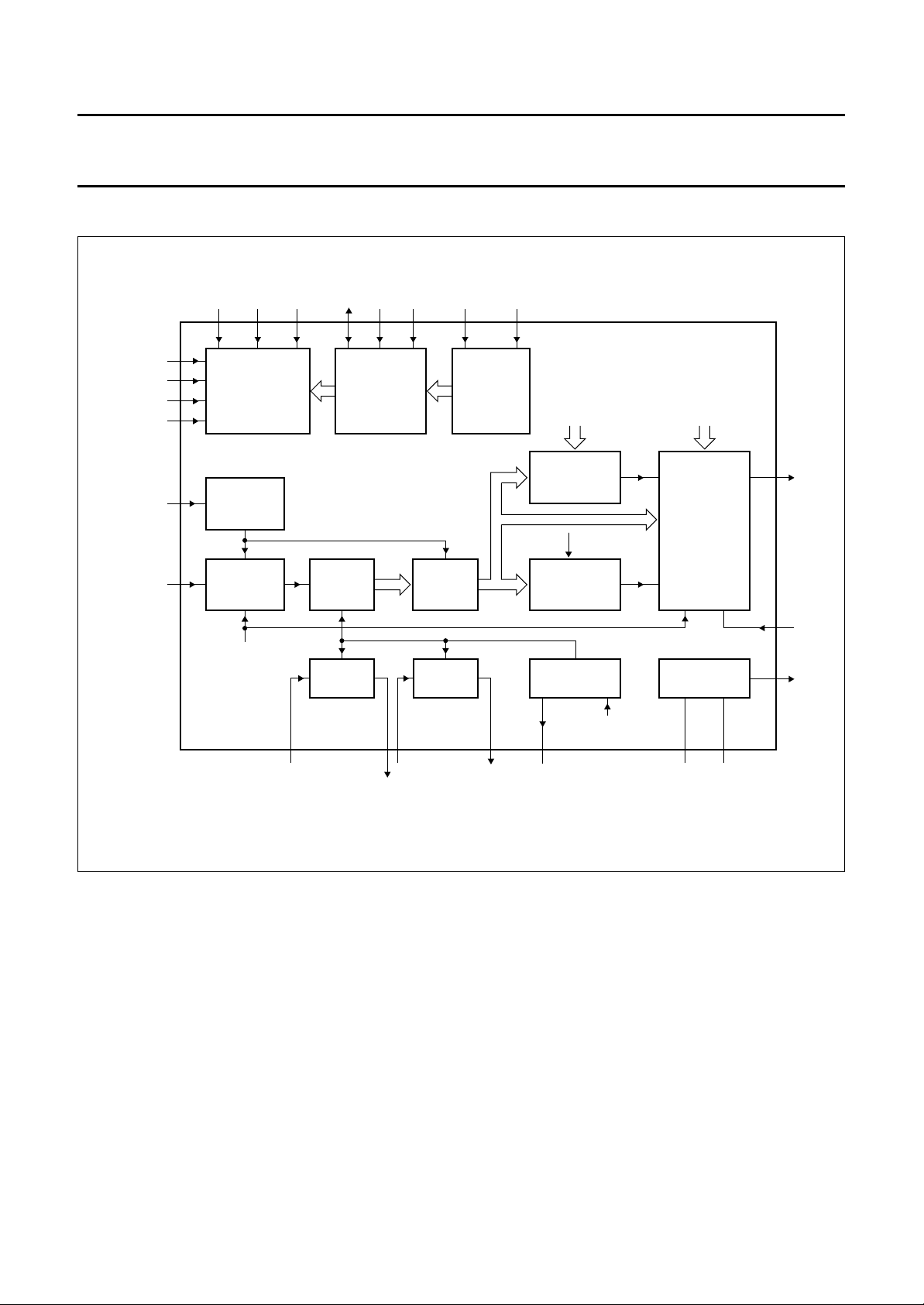
BLOCK DIAGRAM
handbook, full pagewidth
STEEP
LWC
COR
PEAK
SANDCASTLE
input
YIN
AMS CFS FHS
14 8 17
22
4
PIN-TO-I
2
INTERFACE
11
1
SANDCASTLE
DETECTOR
BLACK
5
INSERTION
CLAMP
amplitude
selection
2
C-BUS
SDA
13
CONTROLLER
DELAY
DELAY DELAY IPTAT
UIN
ADR
SCL
12
2
I
C-BUS
VIN VOUT R
UOUT
ADEXT1
6
CLAMPS
3
6-BIT
ADC
ADEXT2
10
line width
STEP
IMPROVEMENT
PROCESSOR
contour filter
selection
CONTOUR
PROCESSOR
line frequency
selection
24918 167
ext
TDA9177
steepness coring peaking
SMART
SHARPNESS
CONTROLLER
BANDGAP
21 19
VCCGND
20
YOUT
15
SNC
23
V
ref
MBH229
Fig.1 Block diagram.
1996 Jun 28 3
Page 4

Philips Semiconductors Preliminary specification
YUV transient improvement processor TDA9177
PINNING
SYMBOL PIN DESCRIPTION
SANDCASTLE 1 sandcastle input
COR 2 coring level input
ADEXT1 3 ADC input 1
LWC 4 line width control input
YIN 5 luminance input
2
ADR 6 I
C-bus address input
UIN 7 colour U input
CFS 8 contour filter select input
VIN 9 colour V input
ADEXT2 10 ADC input 2
PEAK 11 peaking amplitude input
2
SCL 12 serial clock input (I
C-bus)
SDA 13 serial data input/output
2
C-bus)
(I
AMS 14 amplitude select input
SNC 15 smart noise control input
VOUT 16 colour V output
FHS 17 line frequency select input
UOUT 18 colour U output
GND 19 system ground
YOUT 20 luminance output
V
CC
21 supply voltage
STEEP 22 steepness control input
V
ref
R
ext
23 reference voltage output
24 resistor reference
handbook, halfpage
SANDCASTLE
1
COR
2
ADEXT1
LWC
YIN
ADR
3
4
5
6
TDA9177
UIN
7
8
CFS
VIN
9
PEAK
SCL
10
11
12
ADEXT2
Fig.2 Pin configuration.
MBH228
24
23
22
21
20
19
18
17
16
15
14
13
R
ext
V
ref
STEEP
V
CC
YOUT
GND
UOUT
FHS
VOUT
SNC
AMS
SDA
1996 Jun 28 4
Page 5

Philips Semiconductors Preliminary specification
YUV transient improvement processor TDA9177
FUNCTIONAL DESCRIPTION
Y-input selection and amplification
The dynamic range of the luminance input amplifier and
output amplifier can be switched between 0.315 V and
1.0 V typically (excluding sync), either externally
(pin AMS) or by I
2
C-bus (bit AMS of the control register).
Amplitudes outside the corresponding maximum specified
range will be clipped smoothly. The sync part is processed
transparently to the output, independently of the feature
settings. The input is clamped during the HIGH period of
the CLP, defined by the sandcastle reference, and should
be DC-decoupled with an external capacitor. During the
clamp pulse, an artificial black level is inserted in the input
signal to correctly preset the internal circuitry.
The input amplifier drives a delay line of four delay
sections, which form the core of the sharpness
improvement processor.
Sharpness improvement processor
The sharpness improvement processor increases the
slope of large luminance transients of vertical objects and
enhances transients of details in natural scenes by contour
correction. It comprises three main processing units, these
being the step improvement processor, the contour
processor and the smart sharpness controller.
TEP IMPROVEMENT PROCESSOR
S
The step improvement processor (see Fig.9) comprises
two main functions:
1. the MINMAX generator
2. the MINMAX fader.
The MINMAX generator utilizes 5 taps of an embedded
luminance delay line to calculate the minimum and
maximum envelope of all signals momentarily stored in the
delay line. The MINMAX fader chooses between the
minimum and maximum envelopes, depending on the
polarity of a decision signal derived from the contour
processor. Figures 4, 5 and 6 show some waveforms of
the step improvement processor and illustrate that fast
transients result with this algorithm. The MINMAX
generator also outputs a signal that represents the
momentary envelope of the luminance input signal.
This envelope information is used by the smart sharpness
controller.
Limited line width control (also called aperture control) can
be performed externally (pin 4, LWC) or by I2C-bus
(LW-DAC). Line width control can be used to compensate
for horizontal geometry because of the gamma or
blooming of the spot of the CRT.
HE CONTOUR PROCESSOR
T
The contour processor comprises two contour generators
with different frequency characteristics. The contour
generator generates a second-order derivative of the
incoming luminance signal and is used both as a decision
signal for the step improvement processor and as a
luminance correction signal for the smart sharpness
controller. In the smart sharpness controller, this
correction signal is added to the proper delayed original
luminance input signal, making up the peaking signal for
detail enhancement. The peaking path is allowed to select
either the narrow- or wide-peaked contour generators
2
either externally (pin 8, CFS) or by I
C-bus (bit CFS in the
control register). The step improvement circuitry always
selects the wide-peaked contour filter.
The contour generators utilize 3 taps (narrow band) or
5 taps (broad band) of the embedded luminance delay
lines. Figures 11 and 12 illustrate the normalized
frequency transfer of both the narrow and wide contour
filters.
MART SHARPNESS CONTROLLER
S
The smart sharpness controller (see Fig.10) is a fader
circuit that fades between peaked luminance and
step-improved luminance, defined by the output of a step
discriminating device known as the step detector. It also
contains a variable coring level stage.
The step detector behaves like a band-pass filter, so both
amplitude of the step and its slope add to the detection
criterion. The smart sharpness controller has four user
controls:
1. Steepness control
2. Peaking control
3. Coring level control
4. Smart Noise control.
Control settings can be performed either by the I2C-bus or
externally by pin, depending on the status of the I2C-bus
bit STB.
The steepness setting controls the amount of steepness in
the edge-correction processing path. The peaking setting
controls the amount of contour correction for proper detail
enhancement.
The envelope signal generated by the step improvement
processor modulates the peaking setting in order to
reduce the amount of peaking for large sine excursions.
1996 Jun 28 5
Page 6

Philips Semiconductors Preliminary specification
YUV transient improvement processor TDA9177
The coring setting controls the coring level in the peaking
path for rejection of high-frequency noise. All three
settings facilitate reduction of the impact of the sharpness
features, e.g. for noisy luminance signals.
An external noise detector and a user-preferred noise
algorithm are needed to make a fully automatic I2C-bus
controlled smart sharpness control.
An on-board, hard-wired smart sharpness algorithm can
be executed by driving pin SNC with the output of an
external noise detector. This pin, however, is active both in
I2C-bus and pin mode. Figures 13 and 14 illustrate the
impact of the noise control voltage at pin SNC on the user
settings.
Figure 15 shows the relationship between the feature
settings STEEP, COR, PEAK, LWC and their
corresponding pin voltages.
Chrominance compensation
The chrominance delay lines compensate for the delay of
the luminance signal in the step improvement processor,
to ensure a correct colour fit. No delay compensation will
be performed in the chrominance path for line-width
corrections in the luminance path.
Successive approximation ADC
Pins ADEXT1 and ADEXT2 are connected to a 6-bit
successive approximation ADC, via a multiplexer.
The multiplexer toggles between the inputs with each field.
2
I
C-bus
At power up, the bit STB (standby) in the control register is
reset, to leave control to the pins. However, the I2C-bus is
at standby and responds if properly addressed. By setting
STB to logic 1, the control of all features is instead left to
the I2C-bus registers. The PDD bit (Power Down Detected)
in the status register is set each time an interruption of the
supply power occurs and is reset only by reading the
status register. A 3-bit identification code can also be read
from the status register, which can be used to
automatically configure the application by software.
The input control registers can be written sequentially by
the I2C-bus by the embedded automatic subaddress
increment feature or by addressing it directly. The output
control functions cannot be addressed separately.
Reading out the output control functions always starts at
subaddress 00 and all subsequent words are read out by
the automatic subaddress increment procedure. The I2C
address is 40H if pin 6 (ADR) is connected to ground and
E0H if pin 6 (ADR) is connected to pin 23 (V
2
C-bus specification
I
ref
).
Slave address
A6 A5 A4 A3 A2 A1 A0 R/W
ADR1ADR0000X
Auto-increment mode available for subaddresses.
For each field flyback, a conversion is started for either of
the two inputs and the result is stored in the corresponding
bus register, ADEXT1 or ADEXT2.
In this way, any analog, slowly varying signal can be given
2
access to the I
C-bus. If a register access conflict occurs,
the data of that register is made invalid by setting the flag
bit DV (Data Valid) to zero.
1996 Jun 28 6
Page 7

Philips Semiconductors Preliminary specification
YUV transient improvement processor TDA9177
Control functions
FUNCTIONS TYPE SUBADDRESS
DATA BYTE
D7 D6 D5 D4 D3 D2 D1 D0
Inputs
Control REG 00 XXXXCFSFHSAMSSTB
Peaking DAC 01 X X PK5 PK4 PK3 PK2 PK1 PK0
Steepness DAC 02 X X SP5 SP4 SP3 SP2 SP1 SP0
Coring DAC 03 X X CR5 CR4 CR3 CR2 CR1 CR0
Line width DAC 04 X X LW5 LW4 LW3 LW2 LW1 LW0
Outputs
Status REG 00 0000ID2ID1ID0PDD
ADEXT1 (output) REG 01 0 DV AD5 AD4 AD3 AD2 AD1 AD0
ADEXT2 (output) REG 02 0 DV AD5 AD4 AD3 AD2 AD1 AD0
INPUT SIGNALS
Table 1 Address selection
ADR FUNCTION
2
0I
1I
C address is 40H
2
C address is E0H
Table 6 Peaking amplitude
PK5 to PK0 FUNCTION
000000 0%
111111 100%
Table 7 Steepness correction
Table 2 Standby
STB FUNCTION
0 pin mode
2
1I
C-bus mode
Table 3 Amplitude selection
AMS FUNCTION
0 0.315 V luminance
1 1.0 V luminance
Table 4 Line frequency selection
FHS FUNCTION
01f
12f
H
H
Table 5 Contour filter selection
CFS FUNCTION
0 narrow contour filter
1 wide contour filter
SP5 to SP0 FUNCTION
000000 0%
111111 100%
Table 8 Coring level
CR5 to CR0 FUNCTION
000000 0%
111111 100%
Table 9 Line width correction
LW5 to LW0 FUNCTION
000000 0%
111111 100%
O
UTPUT SIGNALS
Table 10 Power Down Detection (PDD)
PDD FUNCTION
0 no power down detected since last read
action
1 power down detected
1996 Jun 28 7
Page 8
Philips Semiconductors Preliminary specification
YUV transient improvement processor TDA9177
Table 11 Identification
(version number or derivative type)
ID2 to ID0 FUNCTION
000 TDA9177/N1
Table 13 Bits AD5 to AD0
AD5 to AD0 FUNCTION
000000B 0 V
111111B 0.5V
ref
Table 12 Data valid of ADC registers
DV FUNCTION
0 data not valid because of possible
register access collision
1 data valid
LIMITING VALUES
In accordance with the Absolute Maximum Rating System (IEC 134).
SYMBOL PARAMETER CONDITIONS MIN. MAX. UNIT
V
CC
V
i
V
o
T
stg
T
amb
supply voltage −0.5 +8.8 V
input voltage on any input −0.5 VCC+ 0.5 V
output voltage of any output −0.5 VCC+ 0.5 V
storage temperature −55 +150 °C
operating ambient temperature −10 +70 °C
QUALITY SPECIFICATION
Quality level in accordance with
“Quality reference Handbook”
“SNW-FQ-611 part E”
. The numbers of the quality specification can be found in the
. The handbook can be ordered using the code 9397 750 00192.
All pins are protected against ESD by means of internal clamping diodes. The protection circuit meets the specification:
Human body model (100 pF,1500 Ω): All pins >3000 V.
Machine model (200 pF, 0 Ω): All pins >300 V.
Latch-up:
At an ambient temperature of 70 °C, all pins meet the specification:
I
> 100 mA or V
trigger
I
< −100 mA or V
trigger
pin
pin
> 1.5V
< −0.5V
CC(max)
CC(max)
THERMAL CHARACTERISTICS
SYMBOL PARAMETER VALUE UNIT
R
th j-a
thermal resistance from junction to ambient in free air <59 K/W
1996 Jun 28 8
Page 9

Philips Semiconductors Preliminary specification
YUV transient improvement processor TDA9177
CHARACTERISTICS
V
=8V; R
CC
SYMBOL PARAMETER CONDITIONS MIN. TYP. MAX. UNIT
Supplies
M
AIN SUPPLY V
V
CC
I
CC
REFERENCE SUPPLY V
V
ref
I
L(max)
RESISTOR REFERENCE R
V
Rref
R
ref
Luminance input/output selection
=10kΩ±2%; T
ref
(PIN 21)
CC
=25°C; unless otherwise specified.
amb
supply voltage 7.2 8.0 8.8 V
supply current 1fH mode − 40 − mA
mode − 45 − mA
2f
H
(PIN 23)
ref
reference supply voltage 3.90 4.00 4.10 V
maximum load current 1.0 −−mA
(PIN 24)
ext
resistor supply voltage − 2 − V
resistor value − 10 − kΩ
L
UMINANCE INPUT YIN (PIN 5)
V
i(Y)
luminance input voltage AMS = LOW − 0.315 0.42 V
AMS = HIGH − 1.0 1.33 V
V
i(Yclamp)
luminance input voltage level during
clamping
I
ib(Y)
luminance input bias current no clamp −−0.1 µA
LUMINANCE INPUT VOLTAGE RANGE SELECTION AMS (PIN 14); note 1
V
AMSL
V
AMSH
input voltage for low luminance range −−0.5 V
input voltage for high luminance
range
− 4.0 − V
3.5 − 5.5 V
1996 Jun 28 9
Page 10

Philips Semiconductors Preliminary specification
YUV transient improvement processor TDA9177
SYMBOL P ARAMETER CONDITIONS MIN. TYP. MAX. UNIT
LUMINANCE OUTPUT YOUT (PIN 20)
V
o(Y) (p-p)
luminance output voltage,
peak-to-peak
V
o(Yclamp)
luminance output voltage during
clamping
S/N(Y) luminance output signal-to-noise ratio 52 −−dB
B
Y
E
bl
E
G(n)
R
out
I
ob
luminance bandwidth 1fH mode (−1 dB);
black level error transparent − 0 1.0 %
nominal gain error transparent − 05%
output resistance −−150 Ω
output bias current 1.3 −−mA
Step improvement
AMS = LOW − 0.315 − V
AMS = HIGH − 1.0 − V
AMS = LOW − 2.35 − V
AMS = HIGH − 2 − V
5 −−MHz
transparent
mode (−1 dB);
2f
H
10 −−MHz
transparent
G
ENERAL
t
r(min)
minimum rise time 10% to 90% 1fH mode; note 2 − 20 − ns
LINE WIDTH CONTROL
δ
(min)
δ
(max)
t
sd(max)
minimum duty factor 2 MHz − 33 − %
maximum duty factor 2 MHz − 67 − %
maximum step displacement 1fH mode − 140 − ns
LINE-WIDTH CONTROL LWC (PIN 4); note 1
V
V
I
bias
i(min)
i(max)
input voltage for minimum line width −−37.5 %V
input voltage for maximum line width 87.5 − 137.5 %V
input bias current − 0.5 −µA
Contour processing
ONTOUR FILTER NARROW-PEAKED
C
f
pc
peaking centre frequency 1f
CONTOUR FILTER WIDE-PEAKED
f
Q
pc1
max
peaking centre frequency 1f
maximum contour amplitude at centre
frequency
mode; note 2 − 20 − ns
2f
H
mode − 70 − ns
2f
H
H
2f
H
H
2f
H
− 3.57 − MHz
− 7.14 − MHz
− 4.14 − MHz
− 8.28 − MHz
note 3 − 12 − dB
ref
ref
1996 Jun 28 10
Page 11

Philips Semiconductors Preliminary specification
YUV transient improvement processor TDA9177
SYMBOL PARAMETER CONDITIONS MIN. TYP. MAX. UNIT
CONTOUR FILTER SELECTION CFS (PIN 8); note 1
V
i(ncf)
V
i(wcf)
Smart sharpness controller
TEP DETECTOR
S
f
dc
CORING
Q
smcL
Q
smcH
CORING LEVEL CONTROL COR (PIN 2); note 1
V
i(min)
V
i(max)
I
bias
PEAKING LEVEL CONTROL PEAK (PIN 11); note 1
V
i(min)
V
i(max)
I
bias
STEEPNESS LEVEL CONTROL STEEP (PIN 22); note 1
V
i(min)
V
i(max)
I
bias
SMART NOISE CONTROL SNC (PIN 15)
V
nfr
V
cfr
I
bias
Overall group delay performance for luminance
t
d
t
de
t
de1
t
de2
input voltage for narrow contour filter −−0.5 V
input voltage for wide contour filter 3.5 − 5.5 V
detection centre frequency 1f
H
2f
H
− 2.13 − MHz
− 4.26 − MHz
minimum coring level note 4 − 0 − %
maximum coring level note 4 − 22 − %
input voltage for minimum coring −−37.5 %V
input voltage for maximum coring 87.5 − 137.5 %V
ref
ref
input bias current −−0.5 µA
input voltage for minimum peaking −−37.5 %V
input voltage for maximum peaking 87.5 − 137.5 %V
ref
ref
input bias current −−0.5 µA
input voltage for minimum steepness −−37.5 %V
input voltage for maximum steepness 87.5 − 137.5 %V
ref
ref
input bias current −−0.5 µA
level for no feature reduction − 0.0 − V
level for complete feature reduction − V
ref
− V
input bias current −−1.0 µA
delay time from input to output 1fH mode − 175 − ns
mode − 108 − ns
2f
H
delay error contour correction 1fH mode; note 5 − 010ns
mode; note 5 − 05ns
2f
H
delay error step correction 1fH mode; note 5 − 010ns
delay error step correction 2fH mode − 05ns
1996 Jun 28 11
Page 12

Philips Semiconductors Preliminary specification
YUV transient improvement processor TDA9177
SYMBOL PARAMETER CONDITIONS MIN. TYP. MAX. UNIT
DELAY TIME SELECTION FHS (PIN 17); note 1
V
i1fH
V
i2fH
input voltage for 1f
input voltage for 2f
H
H
Colour difference processing
OLOUR DIFFERENCE INPUTS UIN AND VIN (PINS 7 AND 9)
C
V
iUIN(p-p)
input voltage range UIN,
peak-to-peak
V
iVIN(p-p)
I
bias
V
cl
input voltage range VIN, peak-to-peak 1.9 −−V
input bias current UIN, VIN no clamp −−0.1 µA
voltage level during clamping − 4.0 − V
COLOUR DIFFERENCE OUTPUTS UOUT AND, VOUT (PINS 18 AND 16)
V
o(cl)
output voltage level during clamping − 3.2 − V
G gain − 1.0 −
E
off
E
G
E
G(UV)
B bandwidth 1f
t
d
R
out
I
ob
offset error transparent − 01%
gain error transparent − 05%
UV gain tracking error transparent − 01%
H
2f
H
delay time 1f
H
2f
H
output resistance −−150 Ω
output bias current 0.5 −−mA
Successive Approximation ADC
−−0.5 V
3.5 − 5.5 V
1.9 −−V
7 −−MHz
7 −−MHz
− 175 − ns
− 108 − ns
ADEXT1
V
FS
I
ib
AND ADEXT2 (PINS 3 AND 10)
full scale input voltage range with respect to GND − 2.0 − V
input bias current −−1µA
data path − 6 − bit
DLE differential linearity error −−1 LSB
ILE integral linearity error −−1 LSB
f
Q
con
adt
conversion frequency each channel − 0.5fV− Hz
conversion time (video lines) each channel − 8 − lines
1996 Jun 28 12
Page 13

Philips Semiconductors Preliminary specification
YUV transient improvement processor TDA9177
SYMBOL PARAMETER CONDITIONS MIN. TYP. MAX. UNIT
Timing
S
ANDCASTLE INPUT SANDCASTLE (PIN 1)
V
scbn
V
scbc
t
scnV
t
scV
V
bkvar
Overall output group delay performance
t
dm(YUV)
Notes
1. This selection is only valid when the standby bit STB is not set.
2. Peaking set to minimum. Input signal is a sine wave with the nominal peak-to-peak amplitude corresponding to the
selected input range.
3. The contour signal cannot be measured separately from the luminance input signal. The contour signal is also
processed by the smart noise controller. The frequency transfer in the peaking mode of the luminance signal can be
derived from the frequency transfer of the selected contour signal, taking into account the summation of the contour
signal and the luminance input signal. The frequency transfer is most easily measured by sine excitation with a
relatively small signal amplitude of 10% of the selected dynamic range of the luminance input, to avoid interaction
with the step detector.
4. The coring level refers to the internally selected contour signal. It is dependent on the contour filter selected and is
specified for the corresponding peaking centre frequency. The coring level can not be measured explicitly at the
luminance output from a big step or sine excitation, because of its interaction with the step detector.
5. Contour correction and step improvement delays are internal delays and cannot be measured in a straightforward
way. Contour correction delay mismatch results in asymmetrical ‘ears’ with respect to the centre of the transient.
Step improvement correction delay mismatch affects the symmetry of the line width control.
detection level for blank no clamping 1.25 1.5 1.75 V
detection level for blank with clamping and w.r.t.
−−0.6 − V
top level sandcastle pulse
input blanking width for no V-sync −−15 µs
input blanking width for V-sync 35 −−µs
ripple on sandcastle burst key level −−0.4 V
delay of matching YUV 1f
H
2f
H
− 010ns
− 05ns
Figures 3 to 8 show the excitation and response of the
TDA9177 sharpness improvement processor. The
excitation shown in Fig.3 is a 2T-pulse, followed by a step
function. Because the TDA9177 can handle both 1fH and
2fH signals, figures illustrating both situations could have
been provided. However, as the difference between these
two modes (with respect to the TDA9177) is that the time
scale of a 2fH response diagram is half that of a 1f
response diagram under equal conditions, only the 1f
H
H
figures are shown.
Figure 4 shows that the step improvement processor does
not affect small amplitudes. Large transients, however,
acquire steeper edges.
1996 Jun 28 13
Figures 5 and 6 show that the width of the signal
processed by the step improvement processor can be
modified by the Line Width Control pin LWC (or DACLW).
Figure 7 shows that the contour processor does not affect
large transients, but works exclusively on small signals,
e.g. details in a video signal.
Figure 8 shows the combination of smart peaking and the
step improvement processor; small signals will be affected
by the contour processor, while large transients will be
modified by the step improvement processor.
Page 14

Philips Semiconductors Preliminary specification
YUV transient improvement processor TDA9177
1000
handbook, halfpage
input
signal
(mV)
800
600
400
200
0
(1) 90% of nominal amplitude.
(2) 30% of nominal amplitude.
(1)
(2)
0 0.5
1.0
MBH230
1.5 2.0
t (µs)
Fig.3 Excitation signals: 90% and 30% of nominal
amplitude 2T-pulse and step function.
1000
handbook, halfpage
V
o
(mV)
800
600
400
200
0
0 0.5
(1) 90% of nominal amplitude.
(2) 30% of nominal amplitude.
(1)
(2)
1.0 1.5 2.0
Fig.4 Response signals for maximum step
improvement, no peaking and nominal line
width.
MBH231
t (µs)
1000
handbook, halfpage
V
o
(mV)
800
600
400
200
0
0 0.5
(1) 90% of nominal amplitude.
(2) 30% of nominal amplitude.
(1)
(2)
1.0 1.5 2.0
Fig.5 Response signals for maximum step
improvement, no peaking and minimum line
width.
MBH232
t (µs)
1000
handbook, halfpage
V
o
(mV)
800
600
400
200
0
0 0.5
(1) 90% of nominal amplitude.
(2) 30% of nominal amplitude.
(1)
(2)
1.0 1.5 2.0
Fig.6 Response signals for maximum step
improvement, no peaking and maximum
line width.
MBH233
t (µs)
1996 Jun 28 14
Page 15

Philips Semiconductors Preliminary specification
YUV transient improvement processor TDA9177
1400
handbook, halfpage
V
o
(mV)
1000
600
200
−200
0 0.5
(1) 90% of nominal amplitude.
(2) 30% of nominal amplitude.
(1)
(2)
1.0 1.5 2.0
MBH234
t (µs)
Fig.7 Response signals for no step improvement,
maximum peaking and 0% coring.
1400
handbook, halfpage
V
o
(mV)
1000
600
200
−200
0 0.5
(1) 90% of nominal amplitude.
(2) 30% of nominal amplitude.
(1)
(2)
1.0 1.5 2.0
Fig.8 Response signals for maximum step
improvement, nominal line width, maximum
peaking and 0% coring.
MBH235
t (µs)
handbook, full pagewidth
YIN
DELAY
CLAMPS
Fig.9 Block diagram of the step improvement processor.
1996 Jun 28 15
MINMAX
SELECTOR
MINMAX
MBH236
line width
control
FADER
Y
envelope
Y
STEP
Page 16

Philips Semiconductors Preliminary specification
YUV transient improvement processor TDA9177
handbook, full pagewidth
100
handbook, full pagewidth
contour
(%)
DETECTOR
FADERCORING
peaking
control
STEP
steepness
control
Y
contour
Y
STEP
delay cells
coring control
smart
noise
Y
c
Fig.10 Block diagram of the smart sharpness controller.
Y
envelope
Y
STEP
MBH237
MBH238
80
60
40
20
0
4
10
(1) 1fH mode.
(2) 2fH mode.
5
10
10
Fig.11 Frequency transfers narrow contour filter.
1996 Jun 28 16
(1) (2)
6
7
10
f (Hz)
8
10
Page 17

Philips Semiconductors Preliminary specification
YUV transient improvement processor TDA9177
100
handbook, full pagewidth
contour
(%)
80
60
40
20
0
4
10
(1) 1fH mode.
(2) 2fH mode.
(1) (2)
5
10
6
10
Fig.12 Frequency transfers wide contour filter.
MBH239
7
10
f (Hz)
8
10
100
handbook, halfpage
(%)
75
50
25
0
0
25 50 100
MBH240
75
V
(%)
ref
Fig.13 Relative decrease of steepness level as a function of voltage at pin SNC starting from four different
steepness level presets.
1996 Jun 28 17
Page 18

Philips Semiconductors Preliminary specification
YUV transient improvement processor TDA9177
100
handbook, halfpage
(%)
80
60
40
20
0
0
25 50 100
MBH241
75
V
(%)
ref
Fig.14 Relative increase of coring level as a function of voltage at pin SNC starting from four different coring level
presets.
100
handbook, halfpage
transfer
(%)
50
0
37.5
50.0 62.5 87.5
MBH242
75
V
(%)
ref
Fig.15 Feature setting control as a function of the pin voltage for peaking, coring, steepness and line width.
1996 Jun 28 18
Page 19

Philips Semiconductors Preliminary specification
YUV transient improvement processor TDA9177
INTERNAL CIRCUITRY
handbook, halfpage
1
SANDCASTLE
Fig.16 Simplified circuit diagram pin 1.
handbook, halfpage
ADEXT1
3
275 Ω
275 Ω
100 kΩ
MBH244
MBH246
handbook, halfpage
COR
Fig.17 Simplified circuit diagram pin 2.
handbook, halfpage
LWC
2
4
275 Ω
MBH245
275 Ω
MBH247
Fig.18 Simplified circuit diagram pin 3.
handbook, halfpage
YIN
5
275 Ω
MBH248
Fig.20 Simplified circuit diagram pin 5.
1996 Jun 28 19
Fig.19 Simplified circuit diagram pin 4.
handbook, halfpage
ADR
6
Fig.21 Simplified circuit diagram pin 6.
275 Ω
MBH249
Page 20

Philips Semiconductors Preliminary specification
YUV transient improvement processor TDA9177
handbook, halfpage
UIN
7
Fig.22 Simplified circuit diagram pin 7.
handbook, halfpage
VIN
9
275 Ω
275 Ω
275 Ω
275 Ω
MBH250
handbook, halfpage
CFS
8
Fig.23 Simplified circuit diagram pin 8.
handbook, halfpage
ADEXT2
10
275 Ω 900 Ω
275 Ω
1 MΩ
MBH251
100 kΩ900 Ω
dbook, halfpage
PEAK
Fig.24 Simplified circuit diagram pin 9.
11
275 Ω
MBH254
Fig.26 Simplified circuit diagram pin 11.
MBH252
Fig.25 Simplified circuit diagram pin 10.
handbook, halfpage
SCL
12
Fig.27 Simplified circuit diagram pin 12.
MBH253
275 Ω
MBH255
1996 Jun 28 20
Page 21

Philips Semiconductors Preliminary specification
YUV transient improvement processor TDA9177
handbook, halfpage
handbook, halfpage
SDA
13
Fig.28 Simplified circuit diagram pin 13.
handbook, halfpage
SNC
15
275 Ω
275 Ω
MBH258
MBH256
AMS
Fig.29 Simplified circuit diagram pin 14.
handbook, halfpage
0.5 mA
14
275 Ω 900 Ω
100 Ω
1 MΩ
16
MBH257
VOUT
MBH259
Fig.30 Simplified circuit diagram pin 15.
handbook, halfpage
FHS
17
275 Ω 900 Ω
1 MΩ
MBH260
Fig.32 Simplified circuit diagram pin 17.
1996 Jun 28 21
Fig.31 Simplified circuit diagram pin 16.
handbook, halfpage
0.5 mA
Fig.33 Simplified circuit diagram pin 18.
100 Ω
18
UOUT
MBH261
Page 22

Philips Semiconductors Preliminary specification
YUV transient improvement processor TDA9177
handbook, halfpage
handbook, halfpage
Fig.34 Simplified circuit diagram pin 19.
handbook, halfpage
GND
V
CC
19
MBH262
0.5 mA
100 Ω
20
MBH263
YOUT
Fig.35 Simplified circuit diagram pin 20.
handbook, halfpage
21
MBH264
STEEP
22
275 Ω
MBH265
Fig.36 Simplified circuit diagram pin 21.
handbook, halfpage
100 Ω
21 kΩ
23
MBH266
V
ref
Fig.38 Simplified circuit diagram pin 23.
1996 Jun 28 22
Fig.37 Simplified circuit diagram pin 22.
handbook, halfpage
100 Ω
Fig.39 Simplified circuit diagram pin 24.
100 Ω
24
MBH267
R
ext
Page 23

Philips Semiconductors Preliminary specification
YUV transient improvement processor TDA9177
2
APPLICATION INFORMATION
The TDA9177 should preferably be used in combination
with the TDA9170 or TDA9170A for making a distinct
improvement to both contrast and sharpness. To benefit
optimally from its picture-sharpening capabilities, the
TDA9177 should be positioned as the last part of the
YUV-chain.
Feature reduction as a function of the noise contents of the
picture can easily be realized in hardware by using the
Noise Detector of the TDA9170A. Smart Noise Control
(SNC) can be tailor-made for each application, by means
2
C-bus control.
of I
Whenever real-time I
embedded smart sharpness algorithm can be executed by
driving pin SNC with the output of the noise detector. In
this concept, additional post-processing of the noise
detector output can easily be realized with external
components.
Figure 40 shows an application example in which the
TDA9177 is bus controlled, with the I2C-bus address at
40H. Furthermore, the Smart Noise Control pin (SNC;
pin 15) is not used in the example shown.
C-bus control is not feasible, the
handbook, full pagewidth
8 V
0 V
YOUT UOUT VOUT
100
100
µF
nF
10
kΩ
24
23 22 21 20 19
18 17 16 15 14 13
TDA9177
1 2 3 4 5 6 7 8 9 10 11 12
sandcastle
100
nF
YIN
UIN
10
nF
VIN SCL SDA
Fig.40 Application diagram.
nF
10
100
100
Ω
Ω
MBH243
1996 Jun 28 23
Page 24

Philips Semiconductors Preliminary specification
YUV transient improvement processor TDA9177
PACKAGE OUTLINE
SDIP24: plastic shrink dual in-line package; 24 leads (400 mil)
D
seating plane
L
Z
24
pin 1 index
e
b
b
1
13
SOT234-1
M
E
A
2
A
A
1
w M
c
E
(e )
M
1
H
1
0 5 10 mm
scale
DIMENSIONS (mm are the original dimensions)
A
A
A
UNIT b
Note
1. Plastic or metal protrusions of 0.25 mm maximum per side are not included.
mm
OUTLINE
VERSION
SOT234-1
max.
4.7 0.51 3.8
12
min.
max.
IEC JEDEC EIAJ
1.3
0.8
b
1
0.53
0.40
REFERENCES
cEe M
0.32
0.23
(1) (1)
D
22.3
21.4
1996 Jun 28 24
9.1
8.7
12
(1)
Z
L
3.2
2.8
EUROPEAN
PROJECTION
M
10.7
10.2
E
12.2
10.5
e
1
w
H
0.181.778 10.16
ISSUE DATE
92-11-17
95-02-04
max.
1.6
Page 25

Philips Semiconductors Preliminary specification
YUV transient improvement processor TDA9177
SOLDERING
Introduction
There is no soldering method that is ideal for all IC
packages. Wave soldering is often preferred when
through-hole and surface mounted components are mixed
on one printed-circuit board. However, wave soldering is
not always suitable for surface mounted ICs, or for
printed-circuits with high population densities. In these
situations reflow soldering is often used.
This text gives a very brief insight to a complex technology.
A more in-depth account of soldering ICs can be found in
our
“IC Package Databook”
Reflow soldering
Reflow soldering techniques are suitable for all QFP
packages.
The choice of heating method may be influenced by larger
plastic QFP packages (44 leads, or more). If infrared or
vapour phase heating is used and the large packages are
not absolutely dry (less than 0.1% moisture content by
weight), vaporization of the small amount of moisture in
them can cause cracking of the plastic body. For more
information, refer to the Drypack chapter in our
Reference Handbook”
Reflow soldering requires solder paste (a suspension of
fine solder particles, flux and binding agent) to be applied
to the printed-circuit board by screen printing, stencilling or
pressure-syringe dispensing before package placement.
Several techniques exist for reflowing; for example,
thermal conduction by heated belt. Dwell times vary
between 50 and 300 seconds depending on heating
method. Typical reflow temperatures range from
215 to 250 °C.
Preheating is necessary to dry the paste and evaporate
the binding agent. Preheating duration: 45 minutes at
45 °C.
(order code 9398 652 90011).
“Quality
(order code 9397 750 00192).
Wave soldering
Wave soldering is not recommended for QFP packages.
This is because of the likelihood of solder bridging due to
closely-spaced leads and the possibility of incomplete
solder penetration in multi-lead devices.
If wave soldering cannot be avoided, the following
conditions must be observed:
• A double-wave (a turbulent wave with high upward
pressure followed by a smooth laminar wave)
soldering technique should be used.
• The footprint must be at an angle of 45° to the board
direction and must incorporate solder thieves
downstream and at the side corners.
Even with these conditions, do not consider wave
soldering the following packages: QFP52 (SOT379-1),
QFP100 (SOT317-1), QFP100 (SOT317-2),
QFP100 (SOT382-1) or QFP160 (SOT322-1).
During placement and before soldering, the package must
be fixed with a droplet of adhesive. The adhesive can be
applied by screen printing, pin transfer or syringe
dispensing. The package can be soldered after the
adhesive is cured.
Maximum permissible solder temperature is 260 °C, and
maximum duration of package immersion in solder is
10 seconds, if cooled to less than 150 °C within
6 seconds. Typical dwell time is 4 seconds at 250 °C.
A mildly-activated flux will eliminate the need for removal
of corrosive residues in most applications.
Repairing soldered joints
Fix the component by first soldering two diagonallyopposite end leads. Use only a low voltage soldering iron
(less than 24 V) applied to the flat part of the lead. Contact
time must be limited to 10 seconds at up to 300 °C. When
using a dedicated tool, all other leads can be soldered in
one operation within 2 to 5 seconds between
270 and 320 °C.
1996 Jun 28 25
Page 26

Philips Semiconductors Preliminary specification
YUV transient improvement processor TDA9177
DEFINITIONS
Data sheet status
Objective specification This data sheet contains target or goal specifications for product development.
Preliminary specification This data sheet contains preliminary data; supplementary data may be published later.
Product specification This data sheet contains final product specifications.
Limiting values
Limiting values given are in accordance with the Absolute Maximum Rating System (IEC 134). Stress above one or
more of the limiting values may cause permanent damage to the device. These are stress ratings only and operation
of the device at these or at any other conditions above those given in the Characteristics sections of the specification
is not implied. Exposure to limiting values for extended periods may affect device reliability.
Application information
Where application information is given, it is advisory and does not form part of the specification.
LIFE SUPPORT APPLICATIONS
These products are not designed for use in life support appliances, devices, or systems where malfunction of these
products can reasonably be expected to result in personal injury. Philips customers using or selling these products for
use in such applications do so at their own risk and agree to fully indemnify Philips for any damages resulting from such
improper use or sale.
2
PURCHASE OF PHILIPS I
C COMPONENTS
2
Purchase of Philips I
components in the I2C system provided the system conforms to the I2C specification defined by
Philips. This specification can be ordered using the code 9398 393 40011.
C components conveys a license under the Philips’ I2C patent to use the
1996 Jun 28 26
Page 27

Philips Semiconductors Preliminary specification
YUV transient improvement processor TDA9177
NOTES
1996 Jun 28 27
Page 28

Philips Semiconductors – a worldwide company
Argentina: see South America
Australia: 34 Waterloo Road, NORTH RYDE, NSW 2113,
Tel. +61 2 9805 4455, Fax. +61 2 9805 4466
Austria: Computerstr. 6, A-1101 WIEN, P.O. Box 213,
Tel. +43 1 60 101, Fax. +43 1 60 101 1210
Belarus: Hotel Minsk Business Center, Bld. 3, r. 1211, Volodarski Str. 6,
220050 MINSK, Tel. +375 172 200 733, Fax. +375 172 200 773
Belgium: see The Netherlands
Brazil: see South America
Bulgaria: Philips Bulgaria Ltd., Energoproject, 15thfloor,
51 James Bourchier Blvd., 1407 SOFIA,
Tel. +359 2 689 211, Fax. +359 2 689 102
Canada: PHILIPS SEMICONDUCTORS/COMPONENTS,
Tel. +1 800 234 7381, Fax. +1 708 296 8556
China/Hong Kong: 501 Hong Kong Industrial Technology Centre,
72 Tat Chee Avenue, Kowloon Tong, HONG KONG,
Tel. +852 2319 7888, Fax. +852 2319 7700
Colombia: see South America
Czech Republic: see Austria
Denmark: Prags Boulevard 80, PB 1919, DK-2300 COPENHAGEN S,
Tel. +45 32 88 2636, Fax. +45 31 57 1949
Finland: Sinikalliontie 3, FIN-02630 ESPOO,
Tel. +358 615 800, Fax. +358 615 80920
France: 4 Rue du Port-aux-Vins, BP317, 92156 SURESNES Cedex,
Tel. +33 1 40 99 6161, Fax. +33 1 40 99 6427
Germany: Hammerbrookstraße 69, D-20097 HAMBURG,
Tel. +49 40 23 52 60, Fax. +49 40 23 536 300
Greece: No. 15, 25th March Street, GR 17778 TAVROS,
Tel. +30 1 4894 339/911, Fax. +30 1 4814 240
Hungary: see Austria
India: Philips INDIA Ltd, Shivsagar Estate, A Block, Dr. Annie Besant Rd.
Worli, MUMBAI 400 018, Tel. +91 22 4938 541, Fax. +91 22 4938 722
Indonesia: see Singapore
Ireland: Newstead, Clonskeagh, DUBLIN 14,
Tel. +353 1 7640 000, Fax. +353 1 7640 200
Israel: RAPAC Electronics, 7 Kehilat Saloniki St, TEL AVIV 61180,
Tel. +972 3 645 0444, Fax. +972 3 648 1007
Italy: PHILIPS SEMICONDUCTORS, Piazza IV Novembre 3,
20124 MILANO, Tel. +39 2 6752 2531, Fax. +39 2 6752 2557
Japan: Philips Bldg 13-37, Kohnan 2-chome, Minato-ku, TOKYO 108,
Tel. +81 3 3740 5130, Fax. +81 3 3740 5077
Korea: Philips House, 260-199 Itaewon-dong, Yongsan-ku, SEOUL,
Tel. +82 2 709 1412, Fax. +82 2 709 1415
Malaysia: No. 76 Jalan Universiti, 46200 PETALING JAYA, SELANGOR,
Tel. +60 3 750 5214, Fax. +60 3 757 4880
Mexico: 5900 Gateway East, Suite 200, EL PASO, TEXAS 79905,
Tel. +1 800 234 7381, Fax. +1 708 296 8556
Middle East: see Italy
Netherlands: Postbus 90050, 5600 PB EINDHOVEN, Bldg. VB,
Tel. +31 40 27 83749, Fax. +31 40 27 88399
New Zealand: 2 Wagener Place, C.P.O. Box 1041, AUCKLAND,
Tel. +64 9 849 4160, Fax. +64 9 849 7811
Norway: Box 1, Manglerud 0612, OSLO,
Tel. +47 22 74 8000, Fax. +47 22 74 8341
Philippines: Philips Semiconductors Philippines Inc.,
106 Valero St. Salcedo Village, P.O. Box 2108 MCC, MAKATI,
Metro MANILA, Tel. +63 2 816 6380, Fax. +63 2 817 3474
Poland: Ul. Lukiska 10, PL 04-123 WARSZAWA,
Tel. +48 22 612 2831, Fax. +48 22 612 2327
Portugal: see Spain
Romania: see Italy
Russia: Philips Russia, Ul. Usatcheva 35A, 119048 MOSCOW,
Tel. +7 095 926 5361, Fax. +7 095 564 8323
Singapore: Lorong 1, Toa Payoh, SINGAPORE 1231,
Tel. +65 350 2538, Fax. +65 251 6500
Slovakia: see Austria
Slovenia: see Italy
South Africa: S.A. PHILIPS Pty Ltd., 195-215 Main Road Martindale,
2092 JOHANNESBURG, P.O. Box 7430 Johannesburg 2000,
Tel. +27 11 470 5911, Fax. +27 11 470 5494
South America: Rua do Rocio 220, 5th floor, Suite 51,
04552-903 São Paulo, SÃO PAULO - SP, Brazil,
Tel. +55 11 821 2333, Fax. +55 11 829 1849
Spain: Balmes 22, 08007 BARCELONA,
Tel. +34 3 301 6312, Fax. +34 3 301 4107
Sweden: Kottbygatan 7, Akalla, S-16485 STOCKHOLM,
Tel. +46 8 632 2000, Fax. +46 8 632 2745
Switzerland: Allmendstrasse 140, CH-8027 ZÜRICH,
Tel. +41 1 488 2686, Fax. +41 1 481 7730
Taiwan: PHILIPS TAIWAN Ltd., 23-30F, 66,
Chung Hsiao West Road, Sec. 1, P.O. Box 22978,
TAIPEI 100, Tel. +886 2 382 4443, Fax. +886 2 382 4444
Thailand: PHILIPS ELECTRONICS (THAILAND) Ltd.,
209/2 Sanpavuth-Bangna Road Prakanong, BANGKOK 10260,
Tel. +66 2 745 4090, Fax. +66 2 398 0793
Turkey: Talatpasa Cad. No. 5, 80640 GÜLTEPE/ISTANBUL,
Tel. +90 212 279 2770, Fax. +90 212 282 6707
Ukraine: PHILIPS UKRAINE, 2A Akademika Koroleva str., Office 165,
252148 KIEV, Tel. +380 44 476 0297/1642, Fax. +380 44 476 6991
United Kingdom: Philips Semiconductors Ltd., 276 Bath Road, Hayes,
MIDDLESEX UB3 5BX, Tel. +44 181 730 5000, Fax. +44 181 754 8421
United States: 811 East Arques Avenue, SUNNYVALE, CA 94088-3409,
Tel. +1 800 234 7381, Fax. +1 708 296 8556
Uruguay: see South America
Vietnam: see Singapore
Yugoslavia: PHILIPS, Trg N. Pasica 5/v, 11000 BEOGRAD,
Tel. +381 11 825 344, Fax.+381 11 635 777
For all other countries apply to: Philips Semiconductors, Marketing & Sales Communications,
Building BE-p, P.O. Box 218, 5600 MD EINDHOVEN, The Netherlands, Fax. +31 40 27 24825
© Philips Electronics N.V. 1996 SCA50
All rights are reserved. Reproduction in whole or in part is prohibited without the prior written consent of the copyright owner.
The information presented in this document does not form part of any quotation or contract, is believed to be accurate and reliable and may be changed
without notice. No liability will be accepted by the publisher for any consequence of its use. Publication thereof does not convey nor imply any license
under patent- or other industrial or intellectual property rights.
Printed in The Netherlands 537021/50/01/pp28 Date of release: 1996 Jun 28 Document order number: 9397 750 00935
Internet: http://www.semiconductors.philips.com/ps/
(1) TDA9177_1 June 26, 1996 11:51 am
 Loading...