

Page 1

INTEGRATED CIRCUITS
DATA SH EET
TDA9171
YUV picture improvement
processor based on histogram
modification and blue stretch
Preliminary specification
Supersedes data of 1995 Aug 01
File under Integrated Circuits, IC02
1996 Jun 17
Page 2
Philips Semiconductors Preliminary specification
YUV picture improvement processor based
TDA9171
on histogram modification and blue stretch
FEATURES
• Picture content dependent non-linear Y and U,V
processing by luminance histogram analysis
• TV standard independent
• Incredible blue stretch
• Optional YC-processing.
GENERAL DESCRIPTION
The TDA9171 is a transparent analog video processor
with YUV input and output interfaces.
The luminance transfer is controlled in a non-linear way by
the distribution, in 5 discrete histogram sections, of the
luminance values measured in a picture. As a result, the
QUICK REFERENCE DATA
SYMBOL PARAMETER MIN. TYP. MAX. UNIT
V
CC
supply voltage 7.2 − 8.8 V
contrast ratio of the most important parts of the scene will
be improved.
So as to maintain a proper colour reproduction the
saturation of the −U and −V colour difference signals are
also controlled as a function of the actual non-linearity in
the luminance channel.
Optionally, the YUV blue stretch circuitry can be activated
which offsets colours near white towards blue.
The supply voltage is 8 V.
The device is contained in a 20 lead dual in-line package.
ORDERING INFORMATION
TYPE
NUMBER
TDA9171 DIP20 plastic dual in-line package; 20 leads; (300 mil); no heat spreader SOT146-1
NAME DESCRIPTION VERSION
PACKAGE
1996 Jun 17 2
Page 3
Philips Semiconductors Preliminary specification
YUV picture improvement processor based
on histogram modification and blue stretch
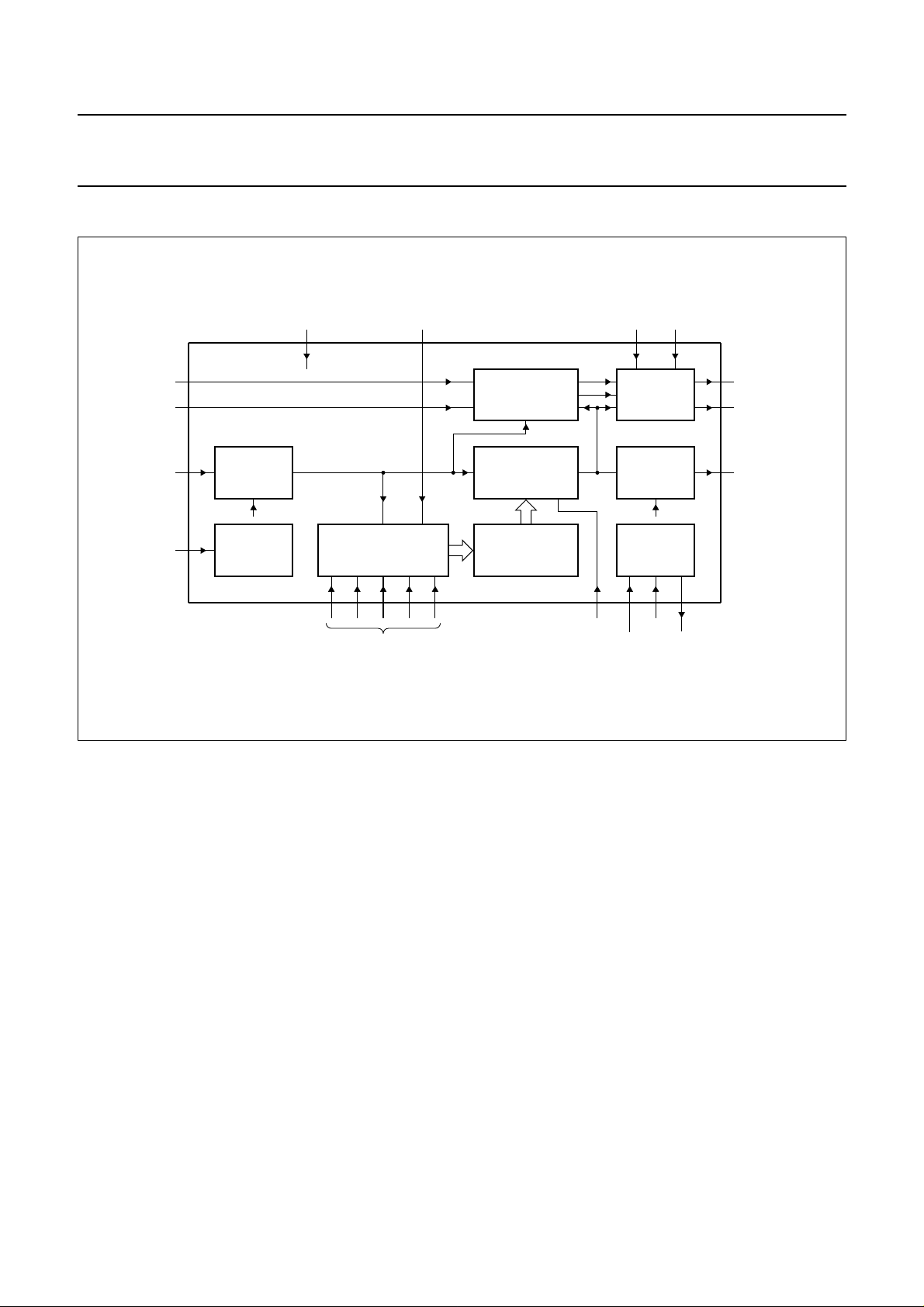
BLOCK DIAGRAM
book, full pagewidth
2
UIN
3
VIN
7
YIN
5
SC
AMPLIFIER
TIMING
CONTROL
INPUT
AND
AMPSEL
AMPSEL
TAUHM BLM BLG
68
TDA9171
HISTOGRAM
MEASUREMENT
9 10 11 12 13
SATURATION
COMPENSATION
NON-LINEAR
AMPLIFIER
HISTOGRAM
PROCESSOR
AMPLIFIER
4
20 1
BLUE
STRETCH
OUTPUT
AMPSEL
SUPPLY
AND
BIASING
16 15 17
TDA9171
19
UOUT
18
VOUT
14
YOUT
MBE990
HM1 to HM5
Fig.1 Block diagram.
NLC
V
EE
CC
V
ref
V
1996 Jun 17 3
Page 4
Philips Semiconductors Preliminary specification
YUV picture improvement processor based
on histogram modification and blue stretch
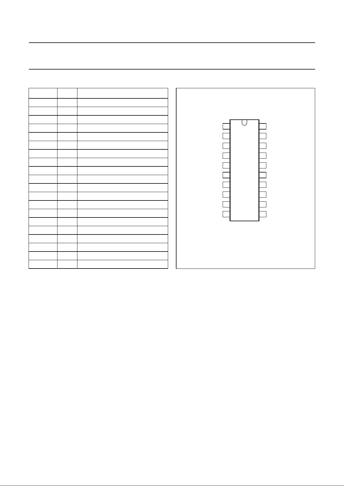
PINNING
SYMBOL PIN DESCRIPTION
BLG 1 blue stretch gain input
UIN 2 U colour difference input −UIN
VIN 3 V colour difference input −VIN
NLC 4 non-linear gain control input
SC 5 sandcastle input
AMPSEL 6 amplitude select input
YIN 7 luminance input
TAUHM 8 time constant histogram input
HM1 9 histogram segment memory 1 input
HM2 10 histogram segment memory 2 input
HM3 11 histogram segment memory 3 input
HM4 12 histogram segment memory 4 input
HM5 13 histogram segment memory 5 input
YOUT 14 luminance output
V
EE
V
CC
V
ref
VOUT 18 colour difference output −VOUT
UOUT 19 colour difference output −UOUT
BLM 20 activation level blue stretch input
15 ground
16 supply voltage
17 reference voltage output
handbook, halfpage
AMPSEL
1
BLG
2
UIN
3
VIN
4
NLC
5
SC
YIN
TAUHM
HM1
HM2
6
7
8
9
10
TDA9171
MBE989
Fig.2 Pin configuration.
TDA9171
20
BLM
19
UOUT
18
VOUT
V
17
ref
V
16
CC
V
15
EE
14
YOUT
13
HM5
12
HM4
11
HM3
FUNCTIONAL DESCRIPTION
Input selection and amplification
The dynamic range of the luminance input amplifier is
0.3 or 1 V (excluding sync) typically, depending on the
logic level at pin AMPSEL (pin 6). Amplitudes which
extend the corresponding specified range will be clipped
smoothly, however, the sync is processed to the output
transparently. The non-linear gain setting will have
minimum effect.
Optionally, in the 1 V input mode, the Y output can be
attenuated by a factor of 0.7 by means of an intermediate
level at pin AMPSEL. This option is meant for correctly
interfacing the combed CVBS signal to the video
processor in a YC-application.
The input is clamped during the logic HIGH period of the
CLP, defined by the sandcastle reference, and should be
DC-decoupled with an external capacitor.
1996 Jun 17 4
Histogram measurement
For the luminance signal the histogram distribution is
measured in real-time over five segments (HM1 to HM5) in
each field. During the period that the luminance is in one
segment, a corresponding external capacitor HMx is
loaded via a current source. At the end of the field five
segment voltages are stored from the external capacitors
into on-board memories. The external capacitors are
discharged and the measurements are repeated.
Parts in the scene that do not contribute to the information
in that scene should be omitted from the histogram
measurement. No measurements are performed during
the blanking period defined by the sandcastle.
The miscount detector disables measurements until it
detects changing parts. Additionally, luminance values
close to full scale (or white) do not contribute as well in
order to maintain the absolute light output. This procedure
is allowed because the eye is less sensitive to detail in
white.
Page 5

Philips Semiconductors Preliminary specification
YUV picture improvement processor based
on histogram modification and blue stretch
As the miscount detector shortens the effective
measurement period and, because of spreads of internal
and external components, the current source is controlled
in a closed-loop to provide a constant value of the sum of
the segment voltages. The dominant time constant of the
closed-loop is external and can be tuned with an
appropriate capacitor value at pin TAUHM (pin 8).
Processing of the measured histogram value
FIELD AVERAGING OF HISTOGRAM VALUES
With very rapid picture changes, also related to the field
interlace, flicker might result. The histogram values are
averaged at the field rate thus reducing the flicker effects.
The time constant of the averaging process is adapted to
the speed of the histogram changes.
DAPTIVE WHITE-POINT STRETCHING
A
For dominant HM4 and HM5 voltages, or large white parts,
the histogram conversion procedure makes a transfer with
large gain in the white parts, however the amount of light
coming out of the scene is considerably reduced. The
white stretcher introduces additional overall gain for
increased light production and, as a result, violates the
principle of having a full scale reference.
S
TANDARD DEVIATION
For scenes, in which segments of the histogram
distribution are very dominant with respect to the others,
the non-linear amplification should be reduced in
comparison to scenes with a flat histogram distribution.
The standard deviation detector measures the spread of
the histogram distribution in the segments HM1 to HM5
and modulates the user setting of the non-linear amplifier.
Non-linear amplifier
The stored segment voltages relative to their average
value, averaged over two fields, determine the individual
gain of each segment in such a way that continuity is
guaranteed for the complete range. The maximum and
minimum gain of each segment is limited. Apart from the
adaptive white-point stretching the black and white
references are not affected by the non-linear processing.
The amount of linearity can be controlled externally by the
NLC pin (Non Linearity Control).
TDA9171
Colour compensation
Non-linear luminance processing influences the colour
reproduction, mainly the colour saturation. Therefore, the
U and V signals are also processed for saturation
compensation.
By convention −U and −V signals must be supplied to the
TDA9171. The −U and −V input signals are clamped
during the logic HIGH period of CLP, defined by the
sandcastle reference. In YC-applications just one colour
difference channel is required for processing the chroma
signal. However, external decoupling capacitors should be
applied to both inputs UIN and VIN. The external coupling
capacitor value should be such that the burst period of the
chroma signal is very softly clamped.
The processing is dependent on the amplitude and sign of
the colour difference signals whenever the blue stretch
circuitry is activated. Therefore, both the polarity and the
nominal amplitude of the colour difference signals are
relevant when using the blue stretch facility.
Blue stretch
The blue stretch circuit is intended to shift colours near
white, with sufficient contrast values, towards more blue
coloured white to give a brighter impression. The
chromaticity shift is proportional to the excess of the
contrast value of a white video signal with respect to a user
adjustable minimum level, defined by a voltage at
pin BLM. In this way blue shift in, for instance, human
faces can be prevented. The global amount of blue shift is
defined by the voltage level at pin BLG. The direction of
shift in the colour triangle is fixed by hardware.
It should be noted that the colour shift is different with a
wrong polarity of the colour difference signals. The
preferred BLG and BLM settings will be related to the
actual nominal amplitudes of the colour difference signals.
The blue stretch facility must be disabled in
YC-applications by setting both BLG and BLM to ground.
1996 Jun 17 5
Page 6

Philips Semiconductors Preliminary specification
YUV picture improvement processor based
TDA9171
on histogram modification and blue stretch
LIMITING VALUES
In accordance with the Absolute Maximum Rating System (IEC 134); all voltages referenced to ground.
SYMBOL PARAMETER MIN. MAX. UNIT
V
CC
V
I/O
T
stg
T
amb
HANDLING
All pins are protected against ESD by means of internal clamping diodes. The protection circuit meets the following
specification:
Human body model: C = 100 pF; R = 1.5 kΩ; all pins >3000 V.
Machine model: C = 200 pF; R = 0 Ω; all pins >300 V.
At an ambient temperature of 90 °C, all pins meet the following specification:
> 100 mA or V
I
trigger
I
<−100 mA or V
trigger
Except for pins 4, 7, 8 and 17 at positive trigger currents:
Pin 4 (NLC): I
Pin 7 (YIN): I
Pin 8 (TAUHM): I
Pin 17 (V
ref
supply voltage −0.5 +8.8 V
supply voltage at any other input or output −0.5 VCC+ 0.5 V
storage temperature −55 +150 °C
operating ambient temperature −10 +70 °C
> 1.5 V
): I
trigger
trigger
trigger
pin
pin
> 90 mA or V
> 90 mA or V
> 90 mA or V
trigger
> 90 mA or V
CC(max)
<−0.5 V
CC(max)
pin
> 1.5V
pin
pin
> 1.5V
> 1.5V
pin
> 1.5V
CC(max)
CC(max)
CC(max)
CC(max)
QUALITY SPECIFICATION
In accordance with SNW-FQ-611 part E. The numbers of the quality specification can be found in the
Handbook”
. The handbook can be ordered using the code 9398 510 63011.
“Quality Reference
1996 Jun 17 6
Page 7

Philips Semiconductors Preliminary specification
YUV picture improvement processor based
TDA9171
on histogram modification and blue stretch
CHARACTERISTICS
=8V; T
V
CC
SYMBOL PARAMETER CONDITIONS MIN. TYP. MAX. UNIT
Supplies
V
CC
I
CC
V
ref
I
load
Luminance input and output selection
L
UMINANCE INPUT (PIN 7)
V
iY(es)
V
iY(cl)
I
Y(bias)
LUMINANCE INPUT VOLTAGE RANGE SELECTION (PIN 6)
V
iAMPSEL(l)
V
iAMPSEL(h)
V
iAMPSEL(m)
I
AMPSEL(bias)
LUMINANCE OUTPUT (PIN 14)
V
oY(es)
V
oY(is)
V
oY(cl)
V
oN
B
Y
B
Y(nl)
E
bl
E
G(n)
C
L
=25°C; unless otherwise specified.
amb
supply voltage 7.2 − 8.8 V
supply current − 35 − mA
reference voltage − 5.0 − V
load current −−1mA
input voltage (excluding sync) V
iAMPSEL
V
iAMPSEL
= low − 0.3 0.45 V
= middle or high − 1.0 1.5 V
input voltage level during clamping − 1.5 − V
input bias current −−0.1 µA
input voltage for lower range V
input voltage for higher range V
input voltage for higher range
iAMPSEL
iAMPSEL
V
iAMPSEL
= low −−0.5 V
= high 3.5 5.0 5.5 V
= middle 1.5 − 2.5 V
including 0.7 attenuation
input bias current −−15 µA
output voltage (excluding sync) V
output voltage (including sync) V
output voltage level during clamping V
iAMPSEL
V
iAMPSEL
iAMPSEL
iAMPSEL
V
iAMPSEL
V
iAMPSEL
output voltage noise with respect to peak
= low − 0.3 − V
= high − 1.0 − V
= middle − 1.0 − V
= low − 2.8 − V
= high − 1.7 − V
= middle − 2.2 − V
−−−52 dB
white
bandwidth minimum NLC gain 8 10 − MHz
bandwidth non-linear processing 10 −−MHz
black level error minimum NLC gain −−1.0 %
nominal gain error minimum NLC gain;
V
iAMPSEL
= low
minimum NLC gain;
V
iAMPSEL
= middle or high
−−7%
−−5%
load capacitance fi= 5 MHz −−25 pF
1996 Jun 17 7
Page 8

Philips Semiconductors Preliminary specification
YUV picture improvement processor based
TDA9171
on histogram modification and blue stretch
SYMBOL PARAMETER CONDITIONS MIN. TYP. MAX. UNIT
Histogram measurement
HISTOGRAM UPDATES AT HMX (PINS 9 TO 13)
Q
HMb
V
HM(av)
V
HM(min)
V
HM(max)
I
HMbias
TIME CONSTANT CONTROL TAUHM (PIN 8)
t
thmr
Q
thms
I
thm(bias)
V
thm(l)
V
thm(h)
MISCOUNT DETECTION
Q
mc(d)
t
d(mcp)
t
mcd(o)
t
mcY
Q
mc(aW)
Q
mc(dW)
Processing of measured histogram values
segment bleeder accuracy −−2%
average voltage level for 5 segments − 1.0 − V
minimum segment voltage level 0 −−V
maximum segment voltage level − 5.0 − V
input bias current −−0.1 µA
response speed see Fig.3 −−−
static error see Fig.4 −−−
input bias current −−0.1 µA
control voltage lower limit − 1.0 − V
control voltage upper limit − 2.0 − V
miscount detection level − 4 − %
miscount propagation delay 20% step − 25 − ns
miscount detection on-time each
− 0.36 −µs
event
mismatch propagation delay and
−−20 ns
luminance delay
miscount activation level at white no miscount − 90 − %
miscount deactivation level at white miscount − 87 − %
W
HITE POINT STRETCH
G
WP
maximum gain luminance for white
maximum NLC gain − 1.1 −
stretch (HM pattern = 00113)
Non-linear amplifier
ON-LINEAR GAIN SET BY HMX (PINS 9 TO 13)
N
Q
nl(b)
G
nlc(min)
segment bleeder accuracy −−3%
minimum gain segment
maximum NLC gain − 0.36 −
(HM pattern = 31100)
G
nlc(max)
maximum gain segment
maximum NLC gain − 2.28 −
(HM pattern = 31100)
NON-LINEAR SETTING NLC (PIN 4)
G
nlc
V
iNLC(l)
V
iNLC(h)
I
iNLC(bias)
non-linear control curve see Fig.5 −−−
control voltage lower limit − 0 − V
control voltage upper limit − 5.0 − V
input bias current −−0.5 µA
1996 Jun 17 8
Page 9

Philips Semiconductors Preliminary specification
YUV picture improvement processor based
TDA9171
on histogram modification and blue stretch
SYMBOL PARAMETER CONDITIONS MIN. TYP. MAX. UNIT
Colour difference processing
COLOUR DIFFERENCE INPUTS UIN AND VIN (PINS 2 AND 3)
V
iU(p-p)
input voltage (pin 2) (peak-to-peak
value)
V
iV(p-p)
input voltage (pin 3) (peak-to-peak
value)
I
UV(bias)
V
iUV(cl)
input bias current (pins 2 and 3) −−0.1 µA
input voltage level during clamping − 1.5 − V
COLOUR DIFFERENCE OUTPUTS UOUT AND VOUT (PINS 19 AND 18)
V
oU
V
oV
V
oUV(cl)
E
os(UV)
output voltage with respect to pin 2 150 −−%
output voltage with respect to pin 3 150 −−%
output voltage level during clamping − 2.3 − V
offset error minimum BLG and BLM;
minimum NLC gain
G
E(UV)
gain error minimum BLG and BLM;
minimum NLC gain
G
M(UV)
gain mismatch minimum BLG and BLM;
minimum NLC gain
B
UV
bandwidth minimum BLG and BLM;
minimum NLC gain
− 1.33 1.8 V
− 1.05 1.8 V
−−1%
−−10 %
−−5%
10 −−MHz
Blue stretch
C
HROMATICITY SHIFT
∆V
oU
variation of U output voltage in white
part of 100% colour bar
∆V
oV
variation of V output voltage in white
part of 100% colour bar
BLUE STRETCH ACTIVATION AREA (PIN 20)
minimum contrast level range see Fig.6 −−−
V
iBLM(l)
V
iBLM(h)
I
BLM(bias)
input control voltage lower limit − 0 − V
input control voltage upper limit − 5.0 − V
input bias current −−0.5 µA
BLUE STRETCH GAIN (PIN 1)
G
BLG
V
iBLG(l)
V
iBLG(h)
I
BLG(bias)
blue stretch gain range see Fig.7 −−−
input voltage lower limit − 0 − V
input voltage upper limit − 5.0 − V
input bias current −−0.5 µA
BLM = 4.06 V −−0.375 − V
BLG = 3.25 V − 0.150 − V
1996 Jun 17 9
Page 10

Philips Semiconductors Preliminary specification
YUV picture improvement processor based
TDA9171
on histogram modification and blue stretch
SYMBOL PARAMETER CONDITIONS MIN. TYP. MAX. UNIT
Timing
SANDCASTLE INPUT (PIN 5)
V
iSC
t
SC(sw)
CLP
PULSE WIDTH RESTORATION
t
CLP(diff)
Overall output performance
T
RANSPARENT MODE (NO BLUE STRETCH; NO NON-LINEAR GAIN)
t
d(YUV)
t
d(YUV)m
input voltage detection level blanking no clamp 1.0 1.25 1.5 V
with clamp 3.5 3.8 4.2 V
input sync width for no vertical sync −−15 µs
for vertical sync 35 −−µs
internal CLP pulse width difference −−30 − %
delay from input to output of YUV
signals
matching of YUV delay minimum BLG and BLM;
minimum BLG and BLM;
minimum NLC gain
− 50 100 ns
− 10 20 ns
minimum NLC gain
80
handbook, halfpage
t
thmr
(ms)
60
40
20
0
0 1000
200 400 600 800
R
= ratio of effective histogram measuring time and active video in one field
miscount
defined by the non-blanking periods of the sandcastle signal in one field.
Fig.3 Response speed of average histogram amplitude control loop as a function of C
at both 50 and 60 Hz field rate (R
miscount
60 Hz 50 Hz
= 1; C
HMx
MBE997
C
TAUHM
= 10 nF).
(nF)
TAUHM
1996 Jun 17 10
Page 11

Philips Semiconductors Preliminary specification
YUV picture improvement processor based
on histogram modification and blue stretch
100
handbook, halfpage
Q
THMS
(%)
80
60
40
20
0
020
R
= ratio of effective histogram measuring time and active video in one field
miscount
defined by the non-blanking periods of the sandcastle signal in one field.
4 8 12 16
W
= t
eff
nonblanking_of_SC
x R
MBE995
miscount
TDA9171
(ms)
Fig.4 Static error on average histogram amplitude (pin TAUHM) as a function of effective histogram
measuring time in a field (C
handbook, halfpage
1
G
NLC
0.75
0.5
0.25
0
1.25 2.25 3.25 5.25
HMx
= 10 nF).
4.25
V
iNLC
MBE996
(V)
Fig.5 Non-linear amplifier gain as a function of input voltage at pin NLC.
1996 Jun 17 11
Page 12

Philips Semiconductors Preliminary specification
YUV picture improvement processor based
on histogram modification and blue stretch
300
handbook, halfpage
V
(mV)
0
−300
−600
−900
1.25 2.05 5.25
∆VOUT
∆UOUT
2.85 3.65 4.45
V
MBE994
iBLM
TDA9171
(V)
UIN =VIN = 0; YIN = 100%; V
Fig.6 Blue stretch activation area as a function of input voltage at pin BLM.
= 3.25 V.
iBLG
handbook, halfpage
300
V
(mV)
0
−300
−600
−900
1.25 2.05 5.25
∆VOUT
∆UOUT
2.85 3.65 4.45
V
MBE993
iBLG
(V)
UIN = VIN = 0; YIN = 100%; V
iBLM
= 4.06 V.
Fig.7 Blue stretch gain as a function of input voltage at pin BLG.
1996 Jun 17 12
Page 13

Philips Semiconductors Preliminary specification
YUV picture improvement processor based
TDA9171
on histogram modification and blue stretch
TEST AND APPLICATION INFORMATION
The TDA9171 is especially designed for YUV applications. A typical application diagram is shown in Fig.8. Jumpers
J1 and J2 can be used to select the appropriate luminance amplitude mode. Potentiometers BLG, BLM and NLC can be
used to apply proper blue stretch and non-linear amplifier control voltages.
The TDA9171 is also prepared for YC-processing. A typical application diagram is shown in Fig.9. Jumpers J1 and J2
can be used to select the appropriate luminance amplitude mode. Potentiometer NLC can be used to apply the proper
non-linear amplifier control voltage. For the chroma processing either the U- or V-channel can be used, however both
channels need to be DC-decoupled and the DC-decoupling capacitor value should be such that the burst period of the
chroma signal Cin is very softly clamped. The blue stretch circuitry cannot be used in YC-applications and should be
switched off by connecting both blue stretch adjustments (BLG and BLG) to ground.
handbook, full pagewidth
470 kΩ
1
UIN UOUT
VIN
SC
J1 J2
180 kΩ
YIN
220 kΩ
10 nF
10 nF
470 kΩ
100 nF
220 nF
10 nF
10 nF
2
3
4
5
TDA9171
6
7
8
9
10
MGD298
BLMBLG
470 kΩ
20
19
100 nF
VOUT
V
CC
GND
YOUT
18
17
16
100 nF
15
14
13
12
11
10 nF
10 nF
10 nF
Fig.8 YUV application.
1996 Jun 17 13
Page 14

Philips Semiconductors Preliminary specification
YUV picture improvement processor based
on histogram modification and blue stretch
handbook, full pagewidth
1
CIN COUT
SC
J1 J2
180 kΩ
YIN
220 kΩ
100 nF
100 nF
NLC
470 kΩ
100 nF
220 nF
10 nF
10 nF
2
3
4
5
TDA9171
6
7
8
9
10
20
19
18
17
16
15
14
13
12
11
MBH500
10 nF
10 nF
10 nF
100 nF
100 nF
V
CC
GND
YOUT
TDA9171
Fig.9 YC application.
1996 Jun 17 14
Page 15

Philips Semiconductors Preliminary specification
YUV picture improvement processor based
on histogram modification and blue stretch
PACKAGE OUTLINE
DIP20: plastic dual in-line package; 20 leads (300 mil)
D
seating plane
L
Z
20
e
b
TDA9171
SOT146-1
M
E
A
2
A
A
1
w M
b
1
11
c
(e )
1
M
H
pin 1 index
1
0 5 10 mm
scale
DIMENSIONS (inch dimensions are derived from the original mm dimensions)
A
A
A
UNIT
inches
Note
1. Plastic or metal protrusions of 0.25 mm maximum per side are not included.
max.
mm
OUTLINE
VERSION
SOT146-1
1 2
min.
max.
1.73
1.30
0.068
0.051
IEC JEDEC EIAJ
b
b
1
0.53
0.38
0.021
0.015
0.014
0.009
REFERENCES
cD E e M
0.36
0.23
(1) (1)
26.92
26.54
1.060
1.045
SC603
6.40
6.22
0.25
0.24
E
10
(1)
M
e
L
1
3.60
8.25
3.05
7.80
0.14
0.32
0.12
0.31
EUROPEAN
PROJECTION
H
E
10.0
0.2542.54 7.62
8.3
0.39
0.010.10 0.30
0.33
ISSUE DATE
w
92-11-17
95-05-24
Z
max.
2.04.2 0.51 3.2
0.0780.17 0.020 0.13
1996 Jun 17 15
Page 16

Philips Semiconductors Preliminary specification
YUV picture improvement processor based
on histogram modification and blue stretch
SOLDERING DIP, SDIP, HDIP, DBS and SIL
Introduction
There is no soldering method that is ideal for all IC
packages. Wave soldering is often preferred when
through-hole and surface mounted components are mixed
on one printed-circuit board. However, wave soldering is
not always suitable for surface mounted ICs, or for
printed-circuits with high population densities. In these
cases reflow soldering is often used.
This text gives a very brief insight to a complex technology.
A more in-depth account of soldering ICs can be found in
“IC Package Databook”
our
Soldering by dip or wave
The maximum permissible temperature of the solder is
260 °C; solder at this temperature must not be in contact
with the joint for more than 5 seconds.
(order code 9398 652 90011).
TDA9171
The total contact time of successive solder waves must not
exceed 5 seconds.
The device may be mounted to the seating plane, but the
temperature of the plastic body must not exceed the
specified storage maximum. If the printed-circuit board has
been pre-heated, forced cooling may be necessary
immediately after soldering to keep the temperature within
the permissible limit.
Repairing soldered joints
Apply a low voltage soldering iron (less than 24 V) to the
lead(s) of the package, below the seating plane or not
more than 2 mm above it. If the temperature of the
soldering iron bit is less than 300 °C it may remain in
contact for up to 10 seconds. If the bit temperature is
between 300 and 400 °C, contact may be up to 5 seconds.
DEFINITIONS
Data sheet status
Objective specification This data sheet contains target or goal specifications for product development.
Preliminary specification This data sheet contains preliminary data; supplementary data may be published later.
Product specification This data sheet contains final product specifications.
Limiting values
Limiting values given are in accordance with the Absolute Maximum Rating System (IEC 134). Stress above one or
more of the limiting values may cause permanent damage to the device. These are stress ratings only and operation
of the device at these or at any other conditions above those given in the Characteristics sections of the specification
is not implied. Exposure to limiting values for extended periods may affect device reliability.
Application information
Where application information is given, it is advisory and does not form part of the specification.
LIFE SUPPORT APPLICATIONS
These products are not designed for use in life support appliances, devices, or systems where malfunction of these
products can reasonably be expected to result in personal injury. Philips customers using or selling these products for
use in such applications do so at their own risk and agree to fully indemnify Philips for any damages resulting from such
improper use or sale.
1996 Jun 17 16
Page 17

Philips Semiconductors Preliminary specification
YUV picture improvement processor based
on histogram modification and blue stretch
NOTES
TDA9171
1996 Jun 17 17
Page 18

Philips Semiconductors Preliminary specification
YUV picture improvement processor based
on histogram modification and blue stretch
NOTES
TDA9171
1996 Jun 17 18
Page 19

Philips Semiconductors Preliminary specification
YUV picture improvement processor based
on histogram modification and blue stretch
NOTES
TDA9171
1996 Jun 17 19
Page 20

Philips Semiconductors – a worldwide company
Argentina: see South America
Australia: 34 Waterloo Road, NORTH RYDE, NSW 2113,
Tel. +61 2 805 4455, Fax. +61 2 805 4466
Austria: Computerstr. 6, A-1101 WIEN, P.O. Box 213,
Tel. +43 1 60 101, Fax. +43 1 60 101 1210
Belarus: Hotel Minsk Business Center, Bld. 3, r. 1211, Volodarski Str. 6,
220050 MINSK, Tel. +375 172 200 733, Fax. +375 172 200 773
Belgium: see The Netherlands
Brazil: see South America
Bulgaria: Philips Bulgaria Ltd., Energoproject, 15thfloor,
51 James Bourchier Blvd., 1407 SOFIA,
Tel. +359 2 689 211, Fax. +359 2 689 102
Canada: PHILIPS SEMICONDUCTORS/COMPONENTS,
Tel. +1 800 234 7381, Fax. +1 708 296 8556
China/Hong Kong: 501 Hong Kong Industrial Technology Centre,
72 Tat Chee Avenue, Kowloon Tong, HONG KONG,
Tel. +852 2319 7888, Fax. +852 2319 7700
Colombia: see South America
Czech Republic: see Austria
Denmark: Prags Boulevard 80, PB 1919, DK-2300 COPENHAGEN S,
Tel. +45 32 88 2636, Fax. +45 31 57 1949
Finland: Sinikalliontie 3, FIN-02630 ESPOO,
Tel. +358 615 800, Fax. +358 615 80920
France: 4 Rue du Port-aux-Vins, BP317, 92156 SURESNES Cedex,
Tel. +33 1 40 99 6161, Fax. +33 1 40 99 6427
Germany: Hammerbrookstraße 69, D-20097 HAMBURG,
Tel. +49 40 23 52 60, Fax. +49 40 23 536 300
Greece: No. 15, 25th March Street, GR 17778 TAVROS,
Tel. +30 1 4894 339/911, Fax. +30 1 4814 240
Hungary: see Austria
India: Philips INDIA Ltd, Shivsagar Estate, A Block, Dr. Annie Besant Rd.
Worli, MUMBAI 400 018, Tel. +91 22 4938 541, Fax. +91 22 4938 722
Indonesia: see Singapore
Ireland: Newstead, Clonskeagh, DUBLIN 14,
Tel. +353 1 7640 000, Fax. +353 1 7640 200
Israel: RAPAC Electronics, 7 Kehilat Saloniki St, TEL AVIV 61180,
Tel. +972 3 645 0444, Fax. +972 3 648 1007
Italy: PHILIPS SEMICONDUCTORS, Piazza IV Novembre 3,
20124 MILANO, Tel. +39 2 6752 2531, Fax. +39 2 6752 2557
Japan: Philips Bldg 13-37, Kohnan 2-chome, Minato-ku, TOKYO 108,
Tel. +81 3 3740 5130, Fax. +81 3 3740 5077
Korea: Philips House, 260-199 Itaewon-dong, Yongsan-ku, SEOUL,
Tel. +82 2 709 1412, Fax. +82 2 709 1415
Malaysia: No. 76 Jalan Universiti, 46200 PETALING JAYA, SELANGOR,
Tel. +60 3 750 5214, Fax. +60 3 757 4880
Mexico: 5900 Gateway East, Suite 200, EL PASO, TEXAS 79905,
Tel. +1 800 234 7381, Fax. +1 708 296 8556
Middle East: see Italy
Netherlands: Postbus 90050, 5600 PB EINDHOVEN, Bldg. VB,
Tel. +31 40 27 83749, Fax. +31 40 27 88399
New Zealand: 2 Wagener Place, C.P.O. Box 1041, AUCKLAND,
Tel. +64 9 849 4160, Fax. +64 9 849 7811
Norway: Box 1, Manglerud 0612, OSLO,
Tel. +47 22 74 8000, Fax. +47 22 74 8341
Philippines: Philips Semiconductors Philippines Inc.,
106 Valero St. Salcedo Village, P.O. Box 2108 MCC, MAKATI,
Metro MANILA, Tel. +63 2 816 6380, Fax. +63 2 817 3474
Poland: Ul. Lukiska 10, PL 04-123 WARSZAWA,
Tel. +48 22 612 2831, Fax. +48 22 612 2327
Portugal: see Spain
Romania: see Italy
Russia: Philips Russia, Ul. Usatcheva 35A, 119048 MOSCOW,
Tel. +7 095 926 5361, Fax. +7 095 564 8323
Singapore: Lorong 1, Toa Payoh, SINGAPORE 1231,
Tel. +65 350 2538, Fax. +65 251 6500
Slovakia: see Austria
Slovenia: see Italy
South Africa: S.A. PHILIPS Pty Ltd., 195-215 Main Road Martindale,
2092 JOHANNESBURG, P.O. Box 7430 Johannesburg 2000,
Tel. +27 11 470 5911, Fax. +27 11 470 5494
South America: Rua do Rocio 220 - 5th floor, Suite 51,
CEP: 04552-903-SÃO PAULO-SP, Brazil, P.O. Box 7383 (01064-970),
Tel. +55 11 821 2333, Fax. +55 11 829 1849
Spain: Balmes 22, 08007 BARCELONA,
Tel. +34 3 301 6312, Fax. +34 3 301 4107
Sweden: Kottbygatan 7, Akalla, S-16485 STOCKHOLM,
Tel. +46 8 632 2000, Fax. +46 8 632 2745
Switzerland: Allmendstrasse 140, CH-8027 ZÜRICH,
Tel. +41 1 488 2686, Fax. +41 1 481 7730
Taiwan: PHILIPS TAIWAN Ltd., 23-30F, 66,
Chung Hsiao West Road, Sec. 1, P.O. Box 22978,
TAIPEI 100, Tel. +886 2 382 4443, Fax. +886 2 382 4444
Thailand: PHILIPS ELECTRONICS (THAILAND) Ltd.,
209/2 Sanpavuth-Bangna Road Prakanong, BANGKOK 10260,
Tel. +66 2 745 4090, Fax. +66 2 398 0793
Turkey: Talatpasa Cad. No. 5, 80640 GÜLTEPE/ISTANBUL,
Tel. +90 212 279 2770, Fax. +90 212 282 6707
Ukraine: PHILIPS UKRAINE, 2A Akademika Koroleva str., Office 165,
252148 KIEV, Tel. +380 44 476 0297/1642, Fax. +380 44 476 6991
United Kingdom: Philips Semiconductors Ltd., 276 Bath Road, Hayes,
MIDDLESEX UB3 5BX, Tel. +44 181 730 5000, Fax. +44 181 754 8421
United States: 811 East Arques Avenue, SUNNYVALE, CA 94088-3409,
Tel. +1 800 234 7381, Fax. +1 708 296 8556
Uruguay: see South America
Vietnam: see Singapore
Yugoslavia: PHILIPS, Trg N. Pasica 5/v, 11000 BEOGRAD,
Tel. +381 11 825 344, Fax.+381 11 635 777
For all other countries apply to: Philips Semiconductors, Marketing & Sales Communications,
Building BE-p, P.O. Box 218, 5600 MD EINDHOVEN, The Netherlands, Fax. +31 40 27 24825
© Philips Electronics N.V. 1996 SCA49
All rights are reserved. Reproduction in whole or in part is prohibited without the prior written consent of the copyright owner.
The information presented in this document does not form part of any quotation or contract, is believed to be accurate and reliable and may be changed
without notice. No liability will be accepted by the publisher for any consequence of its use. Publication thereof does not convey nor imply any license
under patent- or other industrial or intellectual property rights.
Printed in The Netherlands 537021/50/02/pp20 Date of release: 1996 Jun 17 Document order number: 9397 750 00911
Internet: http://www.semiconductors.philips.com/ps/
(1) ADDRESS CONTENT SOURCE June 17, 1996
 Loading...