

Page 1

DATA SH EET
Preliminary specification
File under Integrated Circuits, IC02
1996 Jan 17
INTEGRATED CIRCUITS
TDA9144
I
2
C-bus controlled, alignment-free
PAL/NTSC/SECAM decoder/sync
processor with PALplus helper
demodulator
Page 2

1996 Jan 17 2
Philips Semiconductors Preliminary specification
I2C-bus controlled, alignment-free PAL/NTSC/SECAM
decoder/sync processor with PALplus helper demodulator
TDA9144
FEATURES
• Multi-standard colour decoder and sync processor for
PAL, NTSC and SECAM
• PALplus helper demodulator
• PALplus helper blanking and EDTV-2 blanking
• I2C-bus controlled
• I2C-bus addresses hardware selectable
• Pin compatible with TDA9141
• Alignment free
• Few external components
• Designed for use with baseband delay lines
• Integrated video filters
• Adjustable luminance delay
• Noise detector with I
2
C-bus read-out
• Norm/no_norm detector with I2C-bus read-out
• CVBS or Y/C input, with automatic detection possibility
• CVBS output provided I2C-bus address 8A is used
• Vertical divider system
• Two-level sandcastle signal
• VA synchronization pulse (3-state)
• HA synchronization pulse or clamping pulse CLP
input/output
• Line-locked clock output (6.75 MHz or 6.875 MHz) or
stand-alone I2C-bus output port
• Stand-alone I2C-bus input/output port
• Colour matrix and fast YUV switch
• Comb filter enable input/output with subcarrier
frequency
• Internal bypass mode of external delay line for PALplus
and NTSC applications
• Low power standby mode with 3-state YUV outputs
• Fast blanking detector with I2C-bus read-out
• Blanked or unblanked sync on Y
out
by I2C-bus bit BSY
• internal MACROVISION gating for the horizontal PLL
enabled by bus bit EMG.
GENERAL DESCRIPTION
The TDA9144 is an I
2
C-bus controlled, alignment-free
PAL/NTSC/SECAM decoder/sync processor with helper
demodulator for PALplus signals and blanking facilities for
PALplus and EDTV-2 signals. The TDA9144 has been
designed for use with baseband chrominance delay lines,
and has a combined subcarrier frequency/comb filter
enable signal for communication with a PAL/NTSC comb
filter.
The IC can process both CVBS input signals and Y/C input
signals. The input signal is available on an output pin, in
the event of a Y/C signal, it is added into a CVBS signal.
The sync processor provides a two-level sandcastle, a
horizontal pulse (CLP or HA pulse, bus selectable) and a
vertical (VA) pulse. When the HA pulse is selected, a
line-locked clock (LLC) signal is available at the output port
pin (6.75 MHz or 6.875 MHz).
A fast switch can select either the internal Y signal with the
UV input signals, or YUV signals made of the RGB input
signals. The RGB input signals can be clamped with either
the internal or an external clamping signal.
Two pins with an input/output port and an output port of the
I
2
C-bus are available.
The I2C-bus address of the TDA9144 is hardware
programmable.
The TDA9144 is pin compatible with the TDA9141
(multistandard decoder/sync processor).
ORDERING INFORMATION
TYPE
NUMBER
PACKAGE
NAME DESCRIPTION VERSION
TDA9144 SDIP32 plastic shrink dual in-line package; 32 leads (400 mil) SOT232-1
Page 3
1996 Jan 17 3
Philips Semiconductors Preliminary specification
I2C-bus controlled, alignment-free PAL/NTSC/SECAM
decoder/sync processor with PALplus helper demodulator
TDA9144
QUICK REFERENCE DATA
SYMBOL PARAMETER CONDITIONS MIN. TYP. MAX. UNIT
V
CC
positive supply voltage 7.2 8.0 8.8 V
I
CC
supply current 50 60 70 mA
V
CVBS(p-p)
CVBS input voltage (peak-to-peak value) top sync-white − 1.0 1.43 V
V
Y(p-p)
luminance input voltage
(peak-to-peak value)
top sync-white − 1.0 1.43 V
V
C(p-p)
chrominance burst input voltage
(peak-to-peak value)
− 0.3 0.6 V
V
Y(out)
luminance black-white output voltage − 1.0 − V
V
Y(out)
luminance PALplus output voltage black-white − 0.8 − V
V
Y(out)(p-p)
maximum luminance helper signal output
voltage (peak-to-peak value)
− 686 − mV
V
U(out)(p-p)
U output voltage (peak-to-peak value) standard colour bar − 1.33 − V
V
V(out)(p-p)
V output voltage (peak-to-peak value) standard colour bar − 1.05 − V
V
SC(bl)
sandcastle blanking voltage level 2.2 2.5 2.8 V
V
SC(clamp)
sandcastle clamping voltage level 4.2 4.5 4.8 V
V
VA
VA output voltage 4.0 5.0 5.5 V
V
HA
HA output voltage 4.0 5.0 5.5 V
V
LLC(p-p)
LLC output voltage amplitude
(peak-to-peak value)
250 500 − mV
V
R,G,B(p-p)
RGB input voltage (peak-to-peak value) 0 to 100% saturation − 0.7 1.0 V
V
clamp(I/O)
clamping pulse input/output voltage − 5.0 − V
V
sub(p-p)
subcarrier output voltage amplitude
(peak-to-peak value)
150 200 300 mV
V
OPORT
port output voltage 4.0 5.0 5.5 V
Page 4
1996 Jan 17 4
Philips Semiconductors Preliminary specification
I
2
C-bus controlled, alignment-free PAL/NTSC/SECAM
decoder/sync processor with PALplus helper demodulator
TDA9144
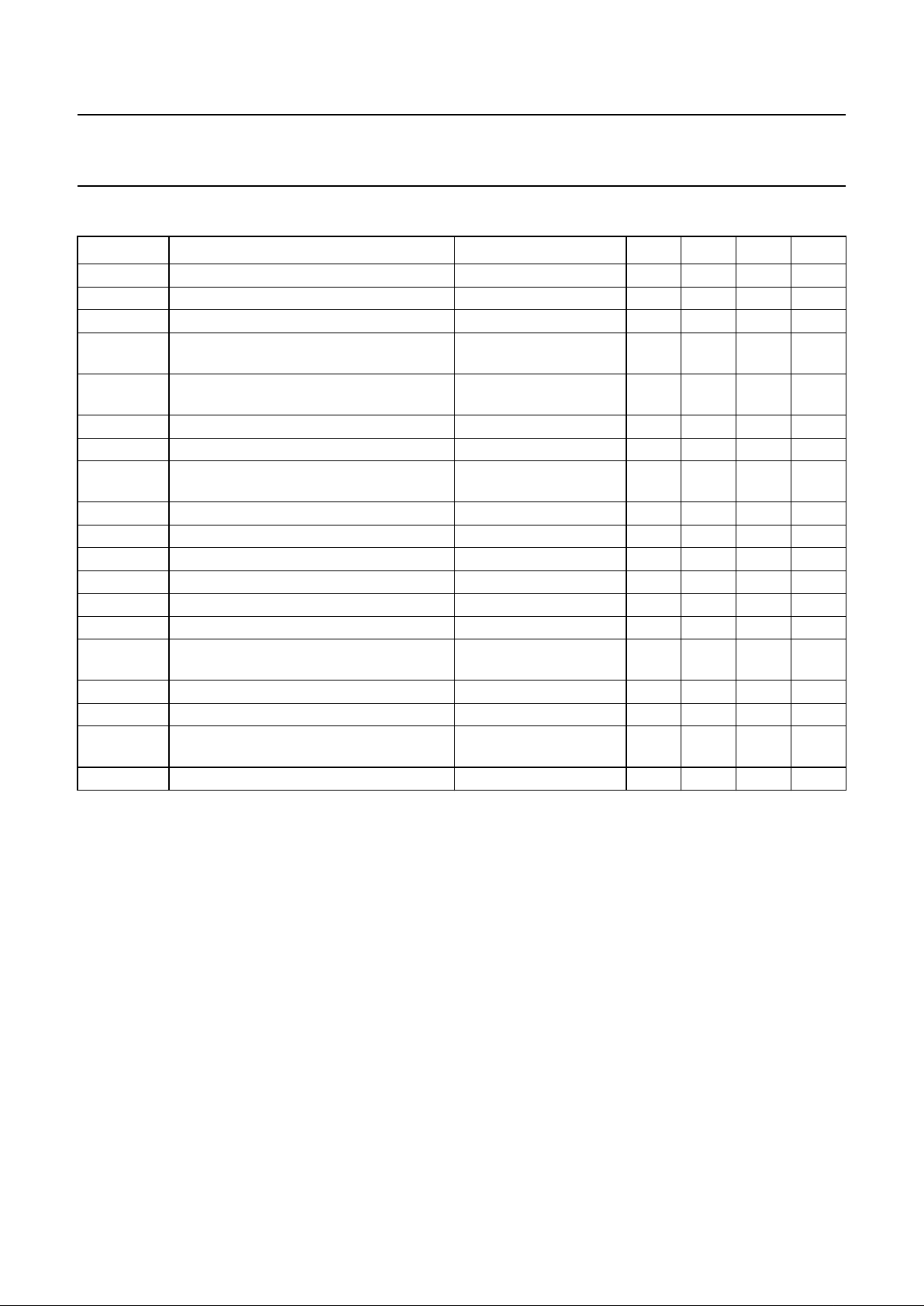
BLOCK DIAGRAM
handbook, full pagewidth
MBG897
I2C-BUS
VERTICAL
SYNC
SEPARATOR
SYNC
SEPARATOR
MATRIX
SWITCH
SWITCH
helper
DELAY
Y CLAMP
ACC
DGND
DEC
C
Y/CVBS
O PORT/LLC
I/O PORT
ADDR (CVBS)
AGND CPLL XTAL XTAL2
SDA SCL
HPLL
SC CLP/HA R G B F
V
CC
FILT
ref
Fscomb
VA
U
out
U
in
V
in
SEC
ref
−(R−Y)
−(B−Y)
V
outYout
LCA
BIAS
TDA9144
INA-INB
HORIZONTAL
PLL
SECAM
CLOCHE
CHROMA
BANDPASS
TRAP
ECL
CLP
VA
HA
ECL
DELAY
HUE
FILTER
TUNING
SECAM
DEMOD
FSC
BUFFER
IDENT
SYSTEM
PAL/NTSC
DEMOD
CHROMA
PLL
CHROMA
SWITCH
TIMING
GENERATOR
TB
BPS
ECMB
YD3−YD0YH1−YH0
18 14 13 12
3
4
2
6
22
15
16
26
25
8
92728 29 30 31 23
1
32
2
57 24
11
17
21 20 19
10
2
Fig.1 Block diagram.
Page 5
1996 Jan 17 5
Philips Semiconductors Preliminary specification
I2C-bus controlled, alignment-free PAL/NTSC/SECAM
decoder/sync processor with PALplus helper demodulator
TDA9144
PINNING
SYMBOL PIN DESCRIPTION
−(R−Y) 1 output signal for −(R−Y)
−(B−Y) 2 output signal for −(B−Y)
U
in
3 chrominance U input
V
in
4 chrominance V input
SCL 5 serial clock input
SDA 6 serial data input/output
V
CC
7 positive supply voltage
DEC 8 digital supply decoupling
DGND 9 digital ground
SC 10 sandcastle output
VA 11 vertical acquisition
synchronization pulse
Y
out
12 luminance output
V
out
13 chrominance V output
U
out
14 chrominance U output
I/O PORT 15 input/output port
O PORT/LLC 16 output port/line-locked clock
output
CLP/HA 17 clamping pulse/HA
synchronization pulse
input/output
F 18 fast switch select input
B 19 BLUE input
G 20 GREEN input
R 21 RED input
ADDR (CVBS) 22 I
2
C-bus address input (CVBS
output)
Fscomb 23 comb filter status input/output
HPLL 24 horizontal PLL filter
C 25 chrominance input
Y/CVBS 26 luminance/CVBS input
AGND 27 analog ground
FILT
ref
28 filter reference decoupling
CPLL 29 colour PLL filter
XTAL 30 reference crystal input
XTAL2 31 second crystal input
SEC
ref
32 SECAM reference decoupling
Fig.2 Pin configuration.
handbook, halfpage
TDA9144
MBG896
1
2
3
4
5
6
7
8
9
10
11
12
13
14
15
16
32
31
30
29
28
27
26
25
24
23
22
21
20
19
18
17
−(B−Y)
−(R−Y)
U
in
V
in
SCL
SDA
V
CC
DEC
DGND
SC
VA
Y
out
V
out
U
out
SEC
ref
XTAL2
XTAL
CPLL
AGND
Y/CVBS
FILT
ref
C
HPLL
Fscomb
ADDR (CVBS)
R
G
B
I/O PORT
O PORT/LLC
F
CLP/HA
Page 6

1996 Jan 17 6
Philips Semiconductors Preliminary specification
I2C-bus controlled, alignment-free PAL/NTSC/SECAM
decoder/sync processor with PALplus helper demodulator
TDA9144
FUNCTIONAL DESCRIPTION
The TDA9144 is an I2C-bus controlled, alignment-free
PAL/NTSC/SECAM colour decoder/sync processor which
has been designed for use with baseband chrominance
delay lines. For PALplus signals, helper demodulation and
blanking facilities are included; for EDTV-2 (60 Hz) signals
only blanking facilities are included.
In the standard operating mode the I2C-bus address is 8A.
If the address input is connected to the positive supply rail
the address will change to 8E.
Input switch
The TDA9144 has a two pin input for CVBS or Y/C signals
which can be selected via the I
2
C-bus. The input selector
also has a position in which it automatically detects
whether a CVBS or Y/C signal is on the input. In this input
selector position, standard identification first takes place
on an added Y/CVBS and C input signal. After that, both
chrominance signal input amplitudes are checked once
and the input with the strongest chrominance burst signal
is selected. The input switch status is read out by the
I2C-bus via output bit YC. The auto input detect mode
indicates YC = 1 for a VBS input signal (no chrominance
component).
CVBS output
In the standard operating mode with I
2
C-bus address 8A,
a CVBS output signal is available on the address pin,
which represents either the CVBS input signal or the Y/C
input signal, added into a CVBS signal.
RGB colour matrix
The TDA9144 has a colour matrix to convert RGB input
signals into YUV signals. A fast switch, controlled by the
signal on pin F and enabled by I
2
C-bus via EFS (enable
fast switch), can select between these YUV signals and
the YUV signals of the decoder. Mode FRGB = 1 (forced
RGB) overrules EFS and forces the matrixed RGB inputs
to the YUV outputs.
CAUTION
The voltage on the chrominance pin must never exceed
5.5 V. If it does, the IC enters a test mode.
CAUTION
The voltage on the Uin pin must never exceed 5.5 V.
If it does, the IC enters a test mode.
The Y signal is internally connected to the switch. The
−(R−Y) and−(B−Y) output signals of the decoder first have
to be delayed in external baseband chrominance delay
lines. The outputs of the delay lines must be connected to
the UV input pins. If the RGB signals are not synchronous
with the selected decoder input signal, clamping of the
RGB input signals is possible by I2C-bus selection of ECL
(external RGB clamp mode) and by feeding an external
clamping signal to the CLP pin. Also in external RGB
clamp mode the VA output will be in a high impedance
OFF-state. The YUV outputs can be put in 3-state mode by
bus bit LPS (low power standby mode).
Standard identification
The standards which the TDA9144 can decode depend
upon the choice of external crystals. If a 4.4 MHz and a
3.6 MHz crystal are used then SECAM, PAL 4.4/3.6 and
NTSC 4.4/3.6 can be decoded. If two 3.6 MHz crystals are
used then only PAL 3.6 and NTSC 3.6 can be decoded.
Which 3.6 MHz standards can be decoded depends upon
the exact frequencies of the 3.6 MHz crystals. In an
application where not all standards are required only one
crystal is sufficient; in this instance the crystal must be
connected to the reference crystal input (pin 30). If a
4.4 MHz crystal is used it must always be connected to the
reference crystal input. Both crystals are used to provide a
reference for the filters and the horizontal PLL, however,
only the reference crystal is used to provide a reference for
the SECAM demodulator. To enable the calibrating circuits
to be adjusted exactly, two bits from I
2
C-bus subaddress
00 are used to indicate which crystals are connected to the
IC.
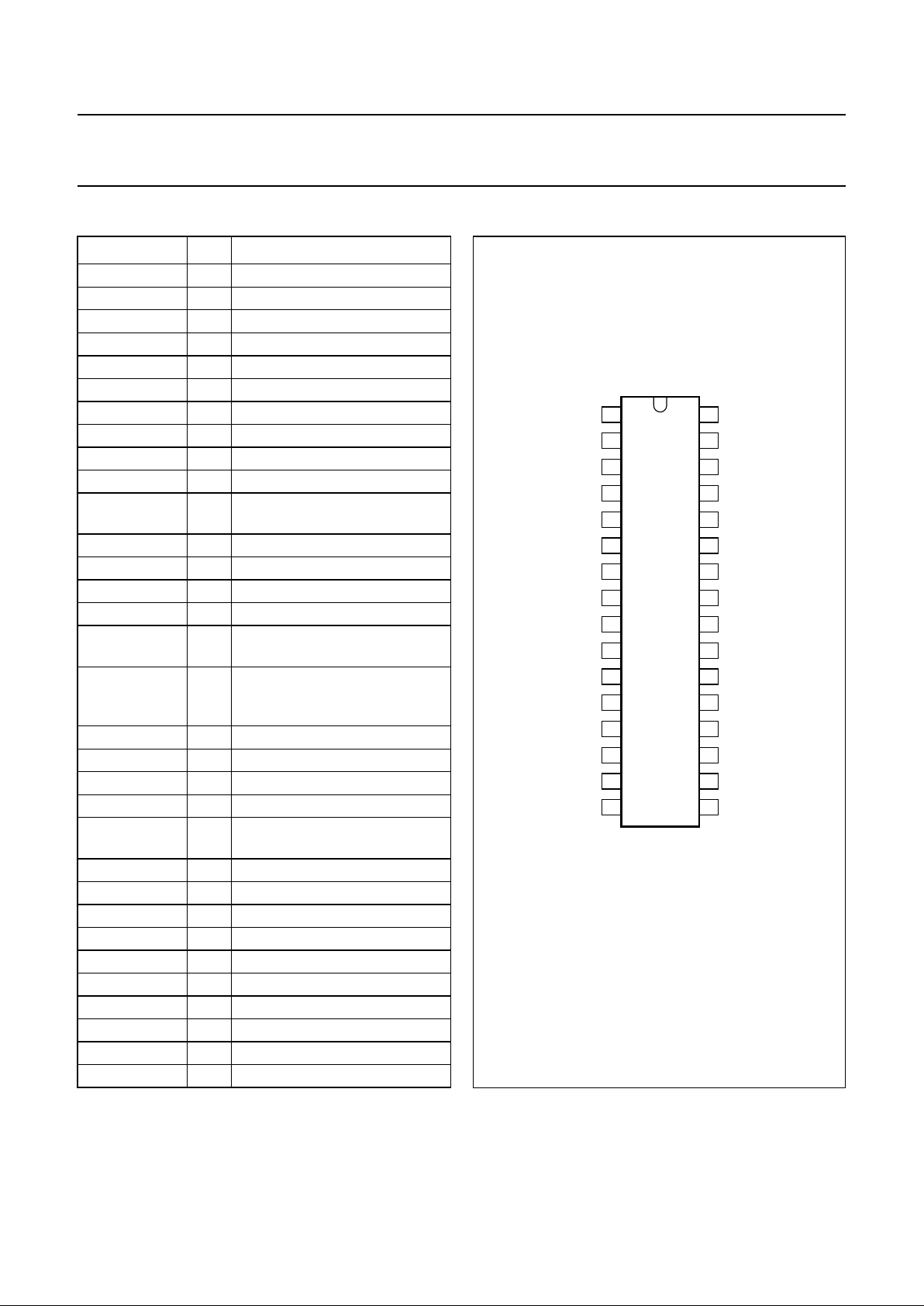
The standard identification circuit is a digital circuit without
external components. The search loop is illustrated
in Fig.3. The decoder (via the I2C-bus) can be forced to
decode either SECAM or PAL/NTSC (but not PAL or
NTSC). Crystal selection can also be forced. Information
concerning standard and which crystal is selected and
whether the colour killer is ON or OFF is provided by the
read out.
Using the forced-mode does not affect the search loop, it
does however, prevent the decoder from reaching or
staying in an unwanted state. The identification circuit
skips impossible standards (e.g. SECAM when no
4.4 MHz crystal is fitted) and illegal standards (e.g. in
forced mode). To reduce the risk of wrong identification
PAL has priority over SECAM. Only line identification is
used for SECAM. For a vertical frequency of 60 Hz
SECAM can be blocked to prevent wrong identification by
means of bus bit SAF.
Page 7
1996 Jan 17 7
Philips Semiconductors Preliminary specification
I2C-bus controlled, alignment-free PAL/NTSC/SECAM
decoder/sync processor with PALplus helper demodulator
TDA9144
Fig.3 Search loop of the identification circuit.
handbook, full pagewidth
PAL
KILLED
PAL
KILLED
PAL
KILLED
NTSC
KILLED
NTSC
KILLED
SECAM
KILLED
Reference crystal Second crystal
MGE040
PAL
NTSC
NTSCPAL
SECAM
c
c
c
c
c
c
c
c
c
c
c
Integrated filters
All chrominance bandpass and notch filters, including the
luminance delay line, are an integral part of the IC. The
filters are gyrator-capacitor type filters. The resonant
frequency of the filters is controlled by a circuit that uses
the active crystal to tune the SECAM Cloche filter during
the vertical flyback time. The remaining filters and the
luminance delay line are matched to this filter. The filters
can be switched to either 4.43 MHz, 4.29 MHz or
3.58 MHz. The switching is controlled by the standard
identification circuit. The luminance notch used for
SECAM has a lower Q-factor than the notch used for
PAL/NTSC. The notches are provided with a little preshoot
to obtain a symmetrical step response. In Y/C mode the
chrominance notch filters are bypassed, to preserve full
signal bandwidth. For a CVBS signal the chrominance
notch filters can be bypassed by bus selection of bit TB
(trap bypass).
The luminance to helper delay difference can be adjusted
by I
2
C-bus, to achieve a correct fitting for the delay in the
PALplus helper demodulation signal path and the
luminance path (not for helper only with trap). The delay of
the colour difference signals −(R−Y) and −(B−Y) in the
chrominance signal path and the external chrominance
delay lines when used, can be fitted to the luminance
signal delay control via I2C-bus in 40 ns steps.
The typical luminance delay can be calculated:
delay ≈ 90 + SAK⋅SBK {170 + 40(FRQ⋅TB)} + 160(YD3) +
160(YD2) + 80(YD1) + 40(YD0) [ns].
Page 8

1996 Jan 17 8
Philips Semiconductors Preliminary specification
I2C-bus controlled, alignment-free PAL/NTSC/SECAM
decoder/sync processor with PALplus helper demodulator
TDA9144
Colour decoder
The PAL/NTSC demodulator employs an oscillator that
can operate with either crystal (3.6 MHz or 4.4 MHz). If the
I2C-bus indicates that only one crystal is connected it will
always connect to the crystal on the reference crystal input
(pin 30). The Hue signal which is adjustable by I2C-bus, is
gated during the burst for NTSC signals.
The SECAM demodulator is an auto-calibrating PLL
demodulator which has two references. The reference
crystal, to force the PLL to the desired free-running
frequency and the bandgap reference, to obtain the
correct absolute value of the output signal. The VCO of the
PLL is calibrated during each vertical blanking period,
when the IC is in search mode or SECAM mode.
If the reference crystal is not 4.4 MHz the decoder will not
produce the correct SECAM signals. Especially for
PALplus and NTSC applications, an internal bypass mode
of the external baseband delay line (for instance
TDA4665) is added, controlled by bus bit BPS (bypass
mode) and has a gain of 2. The bypass mode is not
available for SECAM.
Comb filter interfacing
The frequency of the active crystal is fed to the Fscomb
output, which can be connected to an external comb filter
IC (e.g. SAA4961). When bus bit ECMB is LOW, the
subcarrier frequency is suppressed and its DC value is
LOW. With ECMB HIGH, the DC value is HIGH with the
subcarrier frequency present, and I
2
C-bus output bit YC
and the input switch are always forced in the Y/C mode,
unless an external current sink (e.g. from the comb filter)
prevents this, as pin Fscomb also acts as input pin. In this
event the subcarrier frequency is still present on the same
DC HIGH level
PALplus helper demodulation
PALplus has been introduced to come to an evolutionary
introduction of wide screen transmissions with backward
compatibility with PAL 4 : 3 TV sets. A PALplus signal has
the format of a standard analog PAL composite signal
containing 430 PAL picture lines in letter box format (lines
60 to 274 and 372 to 586), together with helper
information contained in the black bands above and below
the visible letter box area (lines 24 to 59, 336 to 371,
275 to 310, and 587 to 622).
A viewer with a 4 : 3 TV set will see a letter box picture:
black bars of
1
⁄8 picture height at the top as well as at the
bottom with a 16 : 9 picture in between (see left-hand side
picture of Fig.4).
A wide screen viewer without PALplus decoder will only
see the centre picture of Fig.4, or the right hand side
picture when a zoom option is available, however with only
430 lines of vertical resolution.
When a wide screen viewer has a PALplus decoder, it
expands the letter box format to a full-size wide screen
picture with a vertical resolution of 574 lines. The decoder
uses the helper lines information, hidden within the black
bars. See the right-hand side picture of Fig.4.
Furthermore a PALplus signal will deliver full luminance
bandwidth by an Y/C separation technique called ‘Motion
Adaptive Colour Plus’ (MACP). Using this technique, the
signal becomes free from cross colour and cross
luminance. This algorithm requires MACP pre-processing
in the PALplus encoder at the studio output.
The PALplus parts which the TDA9144 processes are in
short:
• Helper demodulation and multiplexing helper with letter
box luminance signal
• Chrominance trap bypassing if necessary
• Creation of reference line 22 (see Fig.5)
• Creation of black set-up and helper set-up
• Correct blanking and timing reference for the necessary
post processing ICs.
Fig.4 Possible PALplus picture displays.
handbook, full pagewidth
430
picture
lines
574
picture
lines
helper lines
helper lines
MBG903
Page 9

1996 Jan 17 9
Philips Semiconductors Preliminary specification
I2C-bus controlled, alignment-free PAL/NTSC/SECAM
decoder/sync processor with PALplus helper demodulator
TDA9144
In case of a PALplus input signal, the standard
identification system of the TDA9144 only determines PAL
and needs additional I2C-bus information for PALplus, via
bus bits MACP, HD, HOB and HBC.
Bus bit MACP determines whether the 4.43 chrominance
signal component of the CVBS input signal should be
suppressed by a 4.43 trap or not. For MACP = 1 the
chrominance suppression takes place outside the
TDA9144.
The HD bit (helper demodulation) enables PALplus helper
demodulation on the U phase (i.e. the B−Y demodulation
axis). As there is only a 4.43 notch for the demodulated
helper, an external notch filter is necessary to suppress the
8.86 MHz demodulation product and resolve the
baseband helper signal. The demodulated helper
luminance signal is always led to a notch filter (4.43 MHz,
no bypass here), then multiplexed with the regular 430
letter box lines luminance signal and led to the output Y
out
.
The black level of the luminance signal is internally
clamped with a large time constant to the black level
generated by the helper demodulator.
Also bus bits HD and MACP determine the presence of a
black set-up voltage (with luminance scaling of a factor
0.8) and a helper set-up voltage for the demodulated
helper signal on the output signal Y
out
. These set-up
voltages are necessary for PALplus signal post processing
outside the TDA9144. The set-up voltages are also
multiplexed into a reference line 22, combined with the
demodulated helper reference of line 23 and luminance
reference of line 623, both present in every PALplus signal
for correct PALplus reference post processing (see Fig.5).
Additional helper blanking bits (HOB, HBC) determine
whether the helper signal has to be blanked or blanked
conditionally depending on the signal-to-noise ratio bit
SNR. Helper blanking can only take place on a norm sync
signal, indicated by output bit NRM = 1. Table 1 is valid in
50 Hz or 60 Hz mode.
Table 1 Helper blanking modes
For EDTV-2 (system M, 60 Hz, 525 lines) outside the letter
box area, blanking is possible and takes place on lines
HOB HBC SNR
HELPER
BLANKING
0 X X OFF
10XON
110OFF
111ON
230 to 312 and 493 to 49
(1)
when helper blanking is
activated.
The TDA9144 can handle PALplus signals in either CVBS
or Y/C format. In case of a Y/C signal, the modulated
helper must be available on the chrominance input pin (C).
The use of the 4.43 trap will not be necessary, as the
chrominance and luminance components of a Y/C signal
are already separated, so the 4.43 trap for the letter box
luminance is bypassed (not for the demodulated helper
signal). During helper demodulation, the internal chroma
bandpass filter is bypassed.
For PALplus the I2C-bus Hue bits HU0 to HU5 are used to
adjust for a correct helper demodulator phase. This has no
effect on the R−Y and B−Y demodulator phase for PAL.
Table 2 gives an overview of the possible PALplus modes
and their effects in the TDA9144. The table is only valid for
a 50 Hz system. In 60 Hz system mode the columns for
line 22, 23b and 623a do not exist, and using the MACP
and HD bits has no effect on the 60 Hz signal.
• Mode 1 → normal PAL
• Mode 2 → PAL with MACP processing
• Mode 3 → full PALplus
• Mode 4 → PALplus without MACP processing (helper
only)
• Mode 5 → near_norm or no_norm sync condition
• Mode 6 → norm sync condition with fast blanking active
• Mode 7 → system ident not identified as PAL.
The indications a and b for the lines 22, 23 and 623
respectively stand for the first half and the second half of a
line.
The signalling bits in line 23 (see Fig.5) are processed in
the same manner as letter box luminance lines in the
TDA9144. Signalling bit decoding and PALplus
identification is done externally with I2C-bus as
communication link to the TDA9144 for bus bits MACP,
HD, HOB, and HBC.
(1) For system M the line numbers start with the first equalizing
pulse in field 1, but the internal line counter starts counting at
the first vertical sync pulse in field 1. This line number
notation is used here and in Fig.9.
Page 10
1996 Jan 17 10
Philips Semiconductors Preliminary specification
I2C-bus controlled, alignment-free PAL/NTSC/SECAM
decoder/sync processor with PALplus helper demodulator
TDA9144
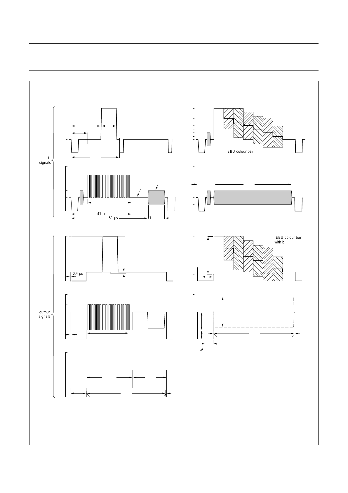
handbook, full pagewidth
1.00
0.30
0
20 µs
32 µs
line 623
(V)
PALplus CVBS in
10 µs
10.5 µs
white level reference
1.00
0.30
0
(V)
EBU colour bar
EBU colour bar
with black set-up
1.00
0.60
0.20
0
(2)
(V)
1.00
0.30
0.45
0.80
0.15
0
(V)
line 23
input
signals
output
signals
41 µs
51 µs
0.4 µs
10.83 µs
PALplus signalling bits
black
level
reference
helper reference
burst −U phase
1.00
0.60
0.77
0.20
0
(V)
line 23
helper
set-up
B
PALplus signalling bits
1.00
0.20
0.60
0
(V)
52 µs
0.15 µs
0.4 µs
686 mV
0.65 µs
52 µs
22 µs30.8 µs
0.15 µs
0.65 µs
baseband helper line with
black and helper set-up
1.00
0.30
0.45
0.15
0
(V)
52 µs
10.5 µs
max. modulated helper line
demodulated helper
area limits
800
mV
delay CLP to set up
(4)
demodulated
helper reference
1.00
0.60
0.20
0
(V)
line 22 reference line
helper set-up
(mid-grey)
black set-up
212 LLC pulses
151 LLC pulses
A
11.2 µs
1.00
0.60
0.20
0
(V)
line 623
black set-up
black
(clamp level)
black level offset
Y
out
(pin 12)
Y black
white level reference
(1)
mid-grey offset = A − B
(3)
MBG904
Fig.5 PALplus CVBS input and Y output signals.
Figures drawn when using subaddress 8A and an Y
delay
of ∼440 ns.
LLC frequency equals 6.875 MHz; 440 LLC pulses per horizontal line.
Demodulated helper shown when using an external 8.8 notch filter.
(1) See Y output parameter Vos in Section “Characteristics”
(2) See demodulated helper parameter td in Section “Characteristics”
(3) See demodulated helper parameter Vos in Section “Characteristics”
(4) See CLP output/HA output parameter td in Section “Characteristics”
Page 11
1996 Jan 17 11
Philips Semiconductors Preliminary specification
I
2
C-bus controlled, alignment-free PAL/NTSC/SECAM
decoder/sync processor with PALplus helper demodulator
TDA9144
Table 2 PALplus modes for 50 Hz
Notes
1. When activated, the black set-up is added to the full frame.
2. When activated, the helper set-up is added to line 22b, 23b, 24 to 59, 275 to 310, 336 to 371, 587 to 622.
3. The 4.43 MHz trap is active in CVBS input mode and TB = 0, otherwise the trap is bypassed.
4. When helper blanking is active (see Table 1) lines 24 to 59, 275 to 310, 336 to 371, 587 to 622 are blanked.
5. Demodulated helper with 400 mV set-up and 4.43 MHz trap active.
6. The 4.43 MHz trap is bypassed during the letter box lines, but activated during helper lines and line 23b to reduce 4.43 MHz rest carrier.
7. The 4.43 MHz trap is active during helper lines and line 23b, during the letter box lines the trap is active when TB = 0.
8. In principle the comb filter should be enabled during letter box lines, when ECMB = 1. It depends on the comb filter if this will be implemented.
9. Line 623a contains luminance in NO_NORM, line 623a is black in a NEAR_NORM sync condition.
MODE MACP HD NRM FBA PAL
4.43
TRAP
COMB
ENABLE
DELAY
LINE
LUMA
AMPL
(b-w)
(V)
BLACK
SET-UP
(1)
(mV)
HELPER
SET-UP
(2)
(mV)
HELPER
LINES
LINE22LINE
23b
LINE
623a
100101TB
(3)
ECMB BPS 1 0 0 luma
(4)
black black black
2 1 0 1 0 1 bypass disabled BPS 0.8 200 0 luma
(4)
set-up helper
(5)
luma
3 1 1 1 0 1 bypass
(6)
disabled bypass 0.8 200 400 helper
(4)
set-up helper luma
401101TB
(7)
disabled
(8)
bypass 0.8 200 400 helper
(4)
set-up helper luma
5XX0XXTB
(3)
ECMB BPS 1 0 0 luma black black luma
(9)
6XX11XTB
(3)
ECMB BPS 1 0 0 luma
(4)
black black black
7XX1X0TB
(3)
ECMB BPS 1 0 0 luma
(4)
black black black
Page 12

1996 Jan 17 12
Philips Semiconductors Preliminary specification
I2C-bus controlled, alignment-free PAL/NTSC/SECAM
decoder/sync processor with PALplus helper demodulator
TDA9144
Fast blanking detector
For PALplus it is necessary to switch-off PALplus as soon
as an external RGB input signal is mixed into a PALplus
signal via a switching signal on the fast blanking input (F).
To detect the presence of a fast blanking signal, a circuit is
added which forces the MACP and HD bit to zero if in more
than one line per field a blanking pulse is detected. More
than one line per field is chosen to prevent switching-off at
every spike detected on the fast blanking input. The
detector output FBA (fast blanking active) can be read-out
by the I
2
C-bus.
Blanked/unblanked sync
By means of the I
2
C-bus bit BSY (blanked sync), output
signal Y
out
will be presented with or without its composite
sync part. At BSY = 0 the composite sync is present on
Y
out
. When activated, helper blanking takes place only
during helper lines scan. At BSY = 1 the black level is filled
in during the line blanking interval and vertical blanking
interval. When activated, the helper blanking extends the
vertical blanking. For PALplus modes with black set-up no
composite sync will be present on Y
out
, independent of the
BSY condition.
Sync processor (ϕ
1
loop)
The main part of the sync circuit is an oscillator running at
440 × f
H
(6.875 MHz), provided that I2C-bus address 8A is
used or 432 × fH (6.75 MHz) for 8E. Its frequency is divided
by 440 or 432 to lock the ϕ1 loop to the incoming signal.
The time-constant of the loop can be selected by the
I2C-bus (fast, auto or slow). In the fast mode the fast
time-constant is chosen independent of signal conditions.
In auto mode the medium time-constant is present with a
fast time constant during the vertical retrace period ('field
boost'). If the noise detector indicates a noisy video signal
the time-constant switches to slow with a smaller field
boost, which is also the time-constant for the slow mode.
In case of a slow time constant sync gating takes place in
a 6 µs window around the separated sync pulse. In case of
no sync lock, both the auto and the slow mode have a
medium time constant, to ensure reliable catching.
The noise content of the video signal is determined by a
noise detector circuit. This circuit measures the noise at
top sync during a 15 line period every field (65 lines after
start VA pulse). When the noise level supersedes the
detector threshold in two consecutive fields, noise is
indicated and bus bit SNR is set.
The free-running frequency of the oscillator is determined
by a digital control circuit that is locked to the active crystal.
When a power-on-reset pulse is detected the frequency of
the oscillator is switched to a frequency of about 10 MHz
(23 kHz horizontal frequency) to protect the horizontal
output transistor. The oscillator frequency is calibrated to
6.875 MHz or 6.75 MHz after receiving data on
subaddress 01 for the first time after power-on-reset
detection.
To ensure that this procedure does not fail it is absolutely
necessary to send subaddress 00 before subaddress 01.
Subaddress 00 contains the crystal indication bits and
when subaddress 01 is received the line oscillator
calibration will be initiated (for the start-up procedure after
power-on-reset detection, see the I
2
C-bus protocol). The
calibration is terminated when the oscillator frequency
reaches 6.875 MHz or 6.75 MHz.
The ϕ1 loop can be opened using the I2C-bus. This is to
facilitate On Screen Display (OSD) information. If there is
no input signal or a very noisy input signal, the ϕ1 loop can
be opened to provide a stable line frequency, and thus a
stable picture.
The sync part also delivers a two-level sandcastle signal,
which provides a combined horizontal and vertical
blanking signal and a clamping pulse for the display
section of the TV.
MACROVISION sync gating
A dedicated gating signal for the separated sync pulses,
starting 11 lines after the detection of a vertical sync pulse
until picture scan starts, can be used to improve the
behaviour of the horizontal PLL with respect to the
unwanted disturbances caused by the pseudo-sync pulses
in video signals with MACROVISION anti-copy guard
signals. This sync gating excludes the pseudo-sync pulses
and can only take place in the auto and fast ϕ
1
time
constant mode, provided I2C-bus bit SNR = 0 and I2C-bus
Page 13
1996 Jan 17 13
Philips Semiconductors Preliminary specification
I2C-bus controlled, alignment-free PAL/NTSC/SECAM
decoder/sync processor with PALplus helper demodulator
TDA9144
bit EMG = 1. I2C-bus bit EMG = 1 enables and EMG = 0
disables this sync gating in the horizontal PLL.
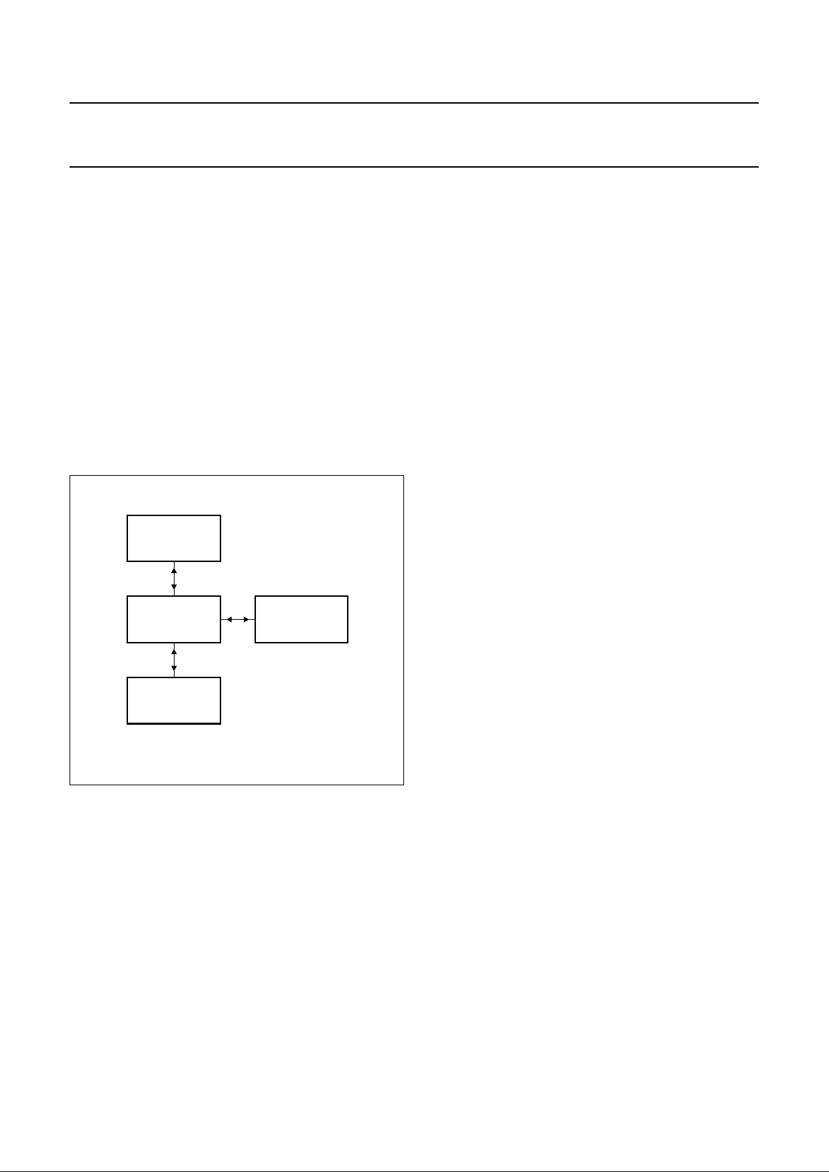
Vertical divider system
The vertical divider system has a fully integrated vertical
sync separator. The divider can accommodate both 50 Hz
and 60 Hz systems; it can either determine the field
frequency automatically or it can be forced to the desired
system via the I
2
C-bus. A block diagram of the vertical
divider system is illustrated in Fig.6.
The divider system operates at twice the horizontal
frequency. The line counter receives enable pulses at this
frequency, thereby counting two pulses per line. A state
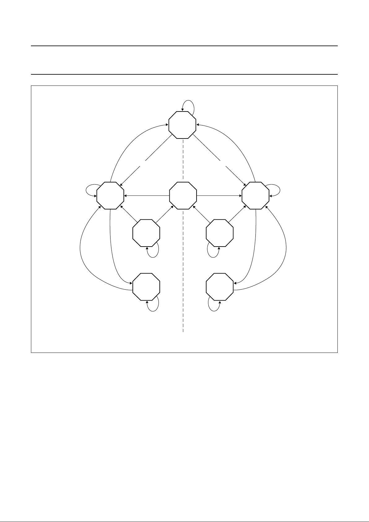
diagram of the controller is shown in Fig.7. Because it is
symmetrical only the right-hand part will be described.
Depending on the previously found vertical frequency, the
controller will be in one of the COUNT states. When the
line counter has counted 488 pulses (i.e. 244 lines of the
video input signal), the controller will move to the next state
depending on the output of the norm counter. This can be
either NORM, NEAR_NORM or NO_NORM, depending
on the position of the vertical sync pulse in the previous
fields. When the controller is in the NORM state it
generates the vertical sync pulse (VSP) automatically and
then, when the line counter is at LC = 626, moves to the
WAIT state. In this condition it waits for the next pulse of
the double line frequency signal, and then moves to the
COUNT state of the current field frequency.
Fig.6 Block diagram of the vertical divider system.
handbook, halfpage
MGE043
NORM COUNTER
CONTROLLER
TIMING
GENERATOR
LINE COUNTER
When the controller returns to the COUNT state, the line
counter will be reset half a line after the start of the vertical
sync pulse of the video input signal. The NORM window
normally looks within one line width and a sudden half line
delay of the vertical sync pulse change can therefore be
neglected, but for PALplus conditions every half line shift
of the vertical sync pulse must be detected. In this case a
half line window is used.
When the controller is in the NEAR_NORM state it will
move to the COUNT state if it detects the vertical sync
pulse within the NEAR_NORM window (i.e.
622 < LC < 628). If no vertical sync pulse is detected the
controller will move back to the COUNT state when the line
counter reaches LC = 628. The line counter will then be
reset.
When the controller is in the NO_NORM state, it will move
to the COUNT state when it detects a vertical sync pulse
and reset the line counter. If a vertical sync pulse is not
detected before LC = 722 (if the ϕ1 loop is locked, even in
forced mode) it will move to the COUNT state and reset the
line counter. If the ϕ1 loop is not locked the controller will
return to the COUNT state when LC = 628.
The forced mode option keeps the controller in either the
left-hand side (60 Hz) or the right-hand side (50 Hz) of the
state diagram.
Figure 8 illustrates the state diagram of the norm counter
which is an up/down counter that increases its counter
value by 1 if it finds a vertical sync pulse within the selected
window. If not it decreases the counter value by 1 (or 2,
see Fig.8). In the NEAR_NORM and NORM states the first
correct vertical sync pulse after one or more incorrect
vertical sync pulses is processed as an incorrect pulse.
This procedure prevents the system from staying in the
NEAR_NORM or NORM state if the vertical sync pulse is
correct in the first field and incorrect in the second field.
In case of no sync lock (SLN = 1) the norm counter is reset
to NO_NORM (wide search window), for fast vertical
catching when switching between video sources. Fast
switching between different channels however can still
result in a continuous horizontal sync lock situation, when
the channel is changed before the norm counter has
reached the NORM state. To provide faster vertical
catching in this case, measures have been taken to
prevent the norm counter to count down to zero before
reaching the NO_NORM state (see left-hand of Fig.8). Bus
bit FWW (forced wide window) enables the norm counter
to stay in the NO_NORM state if desired. The
norm/no_norm status is read out by bus bit NRM.
Page 14
1996 Jan 17 14
Philips Semiconductors Preliminary specification
I2C-bus controlled, alignment-free PAL/NTSC/SECAM
decoder/sync processor with PALplus helper demodulator
TDA9144
Fig.7 State diagram of the vertical divider system.
handbook, full pagewidth
MGE042
WAIT
FOR
RESET
PULSE
NO
NORM
NORM
NORM
COUNTCOUNT
LC = 528 or LC = 576 or on VSP LC = 628 or LC = 722 or on VSP
no_norm
else
no_norm
norm norm
LC < 488
LC ≤ 525 LC ≤ 625
NEAR
NORM
NEAR
NORM
LC < 522 LC < 622
LC < 488
on SYNC
if LC < 576
on SYNC
if LC ≥ 576
LC = 526 LC = 626
on VSP if
522 < LC < 528
or on LC = 528
on VSP if
622 < LC < 628
or on LC = 628
vertical frequency 60 Hz vertical frequency 50 Hz
near_norm near_norm
Page 15

1996 Jan 17 15
Philips Semiconductors Preliminary specification
I2C-bus controlled, alignment-free PAL/NTSC/SECAM
decoder/sync processor with PALplus helper demodulator
TDA9144
Fig.8 State diagram of the norm counter.
(1) VSP found: count 1 up; no VSP found: count 2 down.
handbook, full pagewidth
MGE041
NORM
NO
NORM
NEAR
NORM
NEAR
NORM
NEAR
NORM
22 < NC ≤ 27 0 ≤ NC < 12
10 < NC < 26
(1)
10 < NC < 17
0 < NC < 14
NC = 26
NC = 17
NC = 14
NC = 10
(RESET NC)
NC = 10
(RESET NC)
NC = 22
NC = 0
NC = 12
(RESET NC)
norm test area near_norm test area
Page 16

1996 Jan 17 16
Philips Semiconductors Preliminary specification
I2C-bus controlled, alignment-free PAL/NTSC/SECAM
decoder/sync processor with PALplus helper demodulator
TDA9144
Output port and in/output port
Two stand-alone ports are available for external use.
These ports are I2C-bus controlled, the output port by bus
bit OPB and the input/output port by bus bit OPA. Bus bit
OPA is an open-drain output, to enable input port
functionality. The pin status is read out by bus via output
bit IP.
Sandcastle
Figure 9 illustrates the timing of the acquisition sandcastle
(ASC) and the VA pulse with respect to the input signal.
The sandcastle signal is according to the two-level 5 V
sandcastle format. An external vertical guard current can
overrule the sink current to enable blanking purposes.
handbook, full pagewidth
MBG902
ASC
VA
ASC
ASC
VA
ASC
23
625
312
(1)
262
525
17
280
50 Hz
60 Hz
2nd FIELD 1st FIELD
336
2nd FIELD 1st FIELD
2nd FIELD1st FIELD
2nd FIELD1st FIELD
Fig.9 Acquisition sandcastle signal and VA pulse timing diagram.
(1) See Vertical Section in “Characteristics”
Page 17

1996 Jan 17 17
Philips Semiconductors Preliminary specification
I2C-bus controlled, alignment-free PAL/NTSC/SECAM
decoder/sync processor with PALplus helper demodulator
TDA9144
I2C-bus
For address 8A, an unconnected pin 22 is sufficient as this pin is also a CVBS output. Do not short-circuit the input to
ground. If the address input is connected to the positive supply rail, the address changes from 8A to 8E.
Table 3 Slave address (8A)
Valid subaddresses: 00 to 03 and 17 to 18 (Hex).
Only the five least significant bits of the subaddress bytes are recognized. Auto-increment mode available for
subaddresses. The output addresses 00 and 01 can only be read in auto-increment mode. The I2C-bus transceiver is
designed for a maximum clock frequency (f
SCL
) of 100 kHz.
Table 4 Input bytes
Table 5 Output (status) bytes
Start up procedure: read the status byte until POR = 0; send subaddress 18 with the LPS bit indicating normal operation
(LPS = 0); send subaddress 00 with the crystal indicator bits (XA and XB) indicating that only one crystal is connected
to the IC
(1)
; wait for 50 ms; send subaddress 01; wait for at least 50 ms; set XA,XB to the actual crystal configuration.
Each time before the data in the IC is refreshed, the status byte must be read. If POR = 1, then the above procedure
must be carried out to restart the IC. As long as POR = 1, sending subaddress 01 does not start the line oscillator
calibration. POR is reset when the status register is read out and can only be reset when the supply voltages exceed the
POR detection levels mentioned in the Bias Generator characteristics (see Chapter “Characteristics”).
Failure to stick to the above procedure may result in an incorrect horizontal frequency after power-up or a power-dip.
Remark: if the presence of output signals HA/CLP and/or VA is required after power-up of the IC, subaddress 02 with
the ECL bit indicating ECL = 0 must be sent before sending subaddress 00.
(1) To be absolutely sure that the line oscillator is calibrated with the appropriate crystal frequency data, it is possible to check the
received values of the crystal indication bits via status bits SXA and SXB.
SLAVE ADDRESS A6 A5 A4 A3 A2 A1 A0 R/W
8A 10001X1X
SUB
ADDRESS
MSB DATA BYTE LSB
D7 D6 D5 D4 D3 D2 D1 D0
00 INA INB TB ECMB FOA FOB XA XB
01 FORF FORS OPA OPB POC FM SAF FRQF
02 EFS ECL HU5 HU4 HU3 HU2 HU1 HU0
03 LCA FWW −−−−−−
.........
17 MACP HD HOB HBC BSY YH2 YH1 −
18 BPS LPS FRGB EMG YD3 YD2 YD1 YD0
OUTPUT
ADDRESS
D7 D6 D5 D4 D3 D2 D1 D0
00 POR FSI YC SL IP SAK SBK FRQ
01 −−−FBA NRM SNR SXA SXB
Page 18

1996 Jan 17 18
Philips Semiconductors Preliminary specification
I2C-bus controlled, alignment-free PAL/NTSC/SECAM
decoder/sync processor with PALplus helper demodulator
TDA9144
INPUT SIGNALS
Table 6 Source select; note 1
Note
1. When ECMB = 1 and no current is drawn from the
Fscomb pin, source select is forced to be YC.
Table 7 Trap bypass; note 1
Note
1. The chrominance trap is always bypassed in YC mode
or when MACP = 1.
Table 8 Comb filter enable; note 1
Note
1. MACP = 1 or HD = 1 always enforces ECMB = 0.
Table 9 ϕ
1
time constant
Table 10 Crystal indication
INA INB SOURCE
0 0 CVBS
01YC
1−auto CVBS / YC
TB CONDITION
0 trap not bypassed
1 trap bypassed
ECMB CONDITION
0 comb filter disabled
1 comb filter enabled
FOA FOB MODE
0 0 auto
0 1 slow
1 − fast
XA XB CRYSTAL
002×3.6 MHz
011×3.6 MHz
101×4.4 MHz
111×3.6 MHz and 1 × 4.4 MHz
Table 11 Forced field frequency
Table 12 Output value I/O port
Table 13 Output value O port
Table 14 ϕ
1
loop control
Table 15 Forced standard; note 1
Note
1. If XA and XB indicate that only one crystal is
connected to the IC and FM and FRQF force it to use
the second crystal, then colour will be switched off.
When SAF = 0, SECAM 60 Hz is disabled; when
SAF = 1, SECAM 60 Hz is enabled.
Table 16 Enable fast switch
FORF FORS FIELD FREQUENCY
0 0 auto; 60 Hz if no lock
0 1 60 Hz
1 0 50 Hz
1 1 auto; 50 Hz if no lock
OPA LEVEL
0 LOW
1 HIGH
OPB LEVEL
0 LOW
1 HIGH
POC CONDITION
0 ϕ
1
loop closed
1 ϕ
1
loop open
FM SAF FRQF STANDARD
0 −−auto search
1 0 0 PAL/NTSC second crystal
1 0 1 PAL/NTSC reference crystal
1 1 0 black and white
1 1 1 SECAM reference crystal
EFS CONDITION
0 fast switch disabled
1 fast switch enabled, when FRGB = 0
Page 19

1996 Jan 17 19
Philips Semiconductors Preliminary specification
I2C-bus controlled, alignment-free PAL/NTSC/SECAM
decoder/sync processor with PALplus helper demodulator
TDA9144
Table 17 External RGB clamp mode
Table 18 Forced RGB mode
Table 19 YUV outputs as a function of EFS, FRGB and
Fast switch F
Table 20 Hue
Table 21 Line-locked clock active
Table 22 Forced wide window
Table 23 Motion Adaptive Colour Plus; note 1
Note
1. Black set-up will only be present in a norm sync
condition.
ECL CONDITION
0 off; internal clamp pulse is used
1
on; external clamp pulse has to be supplied
to CLP pin
FRGB CONDITION
0 YUV, when disabled via EFS
1 forced RGB
EFS FRGB F SELECTED INPUTS
00−YUV
− 1 − RGB
100YUV
101RGB
FUNCTION ADDRESS DIGITAL NUMBER
Hue HU5 to HU0 000000 = −45°
111111 = +45°
LCA CONDITION
0 OPB/CLP mode
1 LLC/HA mode
FWW CONDITION
0 auto window mode
1 forced wide window
MACP CONDITION
0 internal 4.43 notch used
1
external MACP chrominance filtering used,
4.43 notch bypassed, black set-up 200 mV
Table 24 PALplus helper demodulator active; note 1
Note
1. Black set-up and helper set-up will only be present in
a norm sync condition.
Table 25 PALplus/EDTV-2 helper blanking (Y, U, V)
Table 26 Blanked sync on Y
out
Note
1. Except for PALplus with black set-up.
Table 27 Luminance to helper delay control
Table 28 Baseband delay line bypass; note 1
Note
1. When HD = 1 the baseband delay line is forced into
bypass mode. SECAM cannot be bypassed.
Table 29 Low power standby mode
HD CONDITION
0off
1
on, PALplus mode with helper set-up
400 mV and black set-up 200 mV
HOB HBC SNR BLANKING
0 −− off
10− on
110 off
111 on
BSY CONDITION
0 unblanked sync; note 1
1 blanked sync
YH2 to YH1 CONDITION
00 −20 ns
11 +25 ns
BPS CONDITION
0 no bypass
1 baseband delay line bypassed
LPS CONDITION
0 normal operation
1 low power standby
Page 20

1996 Jan 17 20
Philips Semiconductors Preliminary specification
I2C-bus controlled, alignment-free PAL/NTSC/SECAM
decoder/sync processor with PALplus helper demodulator
TDA9144
Table 30 Enable MACROVISION gating
Table 31 Luminance delay control
OUTPUT SIGNALS
Table 32 Power-on reset
Table 33 Field frequency indication
Table 34 Input switch mode
Table 35 ϕ
1
lock indication
Table 36 Input value I/O port
EMG CONDITION
0 disable gating
1 enable gating
YD3 to YD0 CONDITION
0000 −280 ns
1111 +160 ns
POR CONDITION
0 normal mode
1 power-down mode
FSI CONDITION
050Hz
160Hz
YC CONDITION
0 CVBS mode
1 Y/C mode
SL CONDITION
0 not locked
1 locked
IP LEVEL
0 LOW
1 HIGH
Table 37 Standard read-out
Table 38 Fast blanking active
Table 39 Norm/no_norm indication in vertical divider
system
Table 40 Signal-to-noise ratio
Table 41 Crystal indication read-out
SAK SBK FRQ STANDARD
0 0 0 PAL second crystal
0 0 1 PAL reference crystal
0 1 0 NTSC second crystal
0 1 1 NTSC reference crystal
1 0 0 illegal forced mode
1 0 1 SECAM reference crystal
11−colour off
FBA CONDITION
0 no fast blanking detected
1 fast blanking detected
NRM CONDITION
0 no_norm or near_norm
1 norm
SNR CONDITION
0 S/N > 20 dB
1 S/N < 20 dB
SXA SXB CRYSTAL
002×3.6 MHz
011×3.6 MHz
101×4.4 MHz
111×3.6 MHz and 1 × 4.4 MHz
Page 21

1996 Jan 17 21
Philips Semiconductors Preliminary specification
I2C-bus controlled, alignment-free PAL/NTSC/SECAM
decoder/sync processor with PALplus helper demodulator
TDA9144
LIMITING VALUES
In accordance with the Absolute Maximum Rating System (IEC 134).
THERMAL CHARACTERISTICS
QUALITY SPECIFICATION
Quality level in accordance with
“SNW-FQ-611-E”
is applicable for ESD protection, human body model: ±3000 V,
100 pF, 1500 Ω on all pins. Machine model: ±300 V, 200 pF, 0 Ω on all pins. The number of the quality specification can
be found in the
“Quality Reference Handbook”
. The handbook can be ordered using the code 9397 750 00192.
SYMBOL PARAMETER CONDITIONS MIN. TYP. MAX. UNIT
V
CC
supply voltage −−9.0 V
I
CC
supply current −−70 mA
P
tot
total power dissipation −−630 mW
T
stg
storage temperature −55 − +150 °C
T
amb
operating ambient temperature −10 − +70 °C
SYMBOL PARAMETER VALUE UNIT
R
th j-a
thermal resistance from junction to ambient in free air 48 K/W
Page 22

1996 Jan 17 22
Philips Semiconductors Preliminary specification
I2C-bus controlled, alignment-free PAL/NTSC/SECAM
decoder/sync processor with PALplus helper demodulator
TDA9144
CHARACTERISTICS
V
CC
=8V; T
amb
=25°C; I2C-bus address 8A; unless otherwise specified.
SYMBOL PARAMETER CONDITIONS MIN. TYP. MAX. UNIT
Supply (pin 7)
V
CC
supply voltage 7.2 8.0 8.8 V
I
CC
supply current 50 60 70 mA
P
tot
total power dissipation 360 480 620 mW
I
CC
low power supply current 12 16 22 mA
Input switch
Caution: the voltage on pin 25 must never exceed 5.5 V, if it does, the IC enters a test mode
Y/CVBS
INPUT (PIN 26)
V
i(p-p)
input voltage (peak-to-peak value) top sync-white − 1.0 1.43 V
Z
i
input impedance 60 −−kΩ
C
i
input capacitance −−5pF
I
i(bias)
input bias current − 3.3 −µA
CINPUT (PIN 25)
V
i(p-p)
input burst voltage
(peak-to-peak value)
− 0.3 0.6 V
Z
i
input impedance 60 −−kΩ
C
i
input capacitance −−5pF
CVBS OUTPUT (PIN 22); ONLY FOR ADDRESS 8A
V
o(p-p)
output voltage (peak-to-peak value) top sync-white − 1.0 − V
Z
o
output impedance −−500 Ω
B bandwidth at −3dB C
L
=15pF 7 −−MHz
V
tsl
top-sync voltage level 2.2 2.8 3.4 V
Bias generator (pin 8)
V
D(DEC)
digital supply voltage 4.8 5.0 5.2 V
V
det(CC)
POR detection level for power supply 5.7 6.0 6.3 V
V
det(DEC)
POR detection level for DEC pin 4.0 4.3 4.6 V
I
L(DEC)
current load on digital supply sum of pins 8, 11, 16, 17 −−2.0 mA
Subcarrier regeneration
G
ENERAL; note 1
CR catching and holding range
reference crystal ±500 −−Hz
second crystal ±450 −−Hz
ϕ phase shift for 80% deviation of
catching range
−−5 deg
Z
i
input impedance
reference crystal and second crystal 0.80 1.00 1.20 kΩ
Page 23

1996 Jan 17 23
Philips Semiconductors Preliminary specification
I2C-bus controlled, alignment-free PAL/NTSC/SECAM
decoder/sync processor with PALplus helper demodulator
TDA9144
FSCOMB OUTPUT (PIN 23)
V
sub(p-p)
subcarrier output voltage amplitude
(peak-to-peak value)
CL= 15 pF 150 200 300 mV
V
cen
comb enable voltage level 4.0 4.2 5.0 V
V
cdis
comb disable voltage level − 0.1 1.4 V
I
sink
sink current to undo forced Y/C mode
of input switch
0.4 − 1.0 mA
R
GND
value of grounded resistor to undo
forced Y/C mode of input switch
4 − 10 kΩ
ACC
ACC control range −20 − +6 dB
change of −(R−Y) and −(B−Y) signals
over range
−−1dB
colour killer treshold
PAL/NTSC −34 −31 −28 dB
SECAM −31 −28 −25 dB
kill/unkill hysteresis − 3 − dB
Demodulators; −(R−Y) and −(B−Y) outputs (pins 1 and 2); demodulated Y
helper
(pin 12)
G
ENERAL
ratio of −(B−Y) to −(R−Y) standard colour bar 1.20 1.27 1.34
TC temperature coefficient of −(R−Y) and
−(B−Y) amplitude
−−0.1 %/K
spread of −(R−Y) to −(B−Y) ratio
between standards
−1 − +1 dB
V
−(R−Y)
output level of −(R−Y) output during
blanking level
1.7 2.1 2.5 V
V
−(B−Y)
output level of −(B−Y) output during
blanking level
1.7 2.0 2.5 V
B bandwidth at −3 dB 600 670 750 kHz
Z
o
output impedance −−500 Ω
∆V
CC
supply voltage dependence −−2 %/V
ϕ hue phase shift note 3 ±35 ±45 ±55 deg
PAL/NTSC
DEMODULATOR
V
−(R−Y)(p-p)
−(R−Y) output voltage
(peak-to-peak value)
standard colour bar 480 540 605 mV
V
−(B−Y)(p-p)
−(B−Y) output voltage
(peak-to-peak value)
standard colour bar 610 685 765 mV
V
res(p-p)
8.8 MHz residue (peak-to-peak value) both outputs −−15 mV
V
res(p-p)
7.2 MHz residue (peak-to-peak value) both outputs −−20 mV
V
res(p-p)
4.4 and 3.6 MHz residue both outputs −−tbf mV
S/N signal-to-noise ratio 0 to 1 MHz 46 −−dB
SYMBOL PARAMETER CONDITIONS MIN. TYP. MAX. UNIT
Page 24

1996 Jan 17 24
Philips Semiconductors Preliminary specification
I2C-bus controlled, alignment-free PAL/NTSC/SECAM
decoder/sync processor with PALplus helper demodulator
TDA9144
PAL DEMODULATOR
V
R(p-p)
1
⁄2H ripple (peak-to-peak value) −−20 mV
ϕ demodulator phase error −−5 deg
SECAM
DEMODULATOR
V
−(R−Y)(p-p)
−(R−Y) output voltage
(peak-to-peak value)
standard colour bar 0.96 1.08 1.21 V
V
−(B−Y)(p-p)
−(B−Y) output voltage
(peak-to-peak value)
standard colour bar 1.22 1.37 1.53 V
f
os
black level offset frequency −−7 kHz
S/N signal-to-noise ratio 0 to 1 MHz 40 −−dB
V
res(p-p)
7.8 MHz to 9.4 MHz residue
(peak-to-peak value)
−−30 mV
f
pole
pole frequency of de-emphasis 77 85 93 kHz
ratio of pole and zero frequency − 3 −
V
cal
calibration voltage 345V
NL non linearity −−3%
D
EMODULATED HELPER (PIN 12)
V
Y(p-p)
helper output voltage
(peak-to-peak value)
PALplus limits 610 686 770 mV
V
Y(p-p)
helper set-up amplitude only helper lines, line 22 and
line 23
380 400 420 mV
t
d
group delay within passband −−10 ns
ϕ demodulator phase including
1
⁄2H error −−5 deg
α
c(M/D)
crosstalk modulated helper to
demodulated sign
0 to 1 MHz −36 −−dB
4.43 MHz residue −36 −−dB
THD total harmonic distortion in ACC −36 −−dB
t
Y
helper output timing to Y
out
−−10 ns
V
os
offset demodulator mid-grey to
inserted mid-grey level
mid-grey line 23 and line 22;
see Fig.5
−−5mV
t
su
helper set-up width (363 LLC pulses)
and start helper set-up
− 52.8 −µs
t
d
delay between mid-sync of input and
start helper set-up
YD3 to YD0 = 1011; note 4;
see Fig.5
− 8.8 −µs
t
d
delay between start black set-up and
start helper set-up (212 LLC pulses)
only line 22 and 23 − 30.8 −µs
B baseband helper bandwidth at −3dB − 2.6 − MHz
Filters
T
UNING
V
tune
tuning voltage 1.5 3 6 V
SYMBOL PARAMETER CONDITIONS MIN. TYP. MAX. UNIT
Page 25

1996 Jan 17 25
Philips Semiconductors Preliminary specification
I2C-bus controlled, alignment-free PAL/NTSC/SECAM
decoder/sync processor with PALplus helper demodulator
TDA9144
LUMINANCE DELAY; YD3 to YD0 = 1011; YH2 to YH1 = 01
t
d(on)
delay time colour on fsc= 3.6 MHz; TB = 0 555 580 605 ns
f
sc
= 3.6 MHz and 4.4 MHz;
TB = 1
515 540 565 ns
t
d(off)
delay time colour off 350 370 390 ns
t
d(tun)
delay time tuning range 15 steps YD3 to YD0; note 2 −280 − +160 ns
t
d(tun)
Y to helper delay tuning range 3 steps YH2 to YH1 −20 − +25 ns
CHROMINANCE TRAP
f
o
notch frequency fsc= 3.6 MHz 3.53 3.58 3.63 MHz
f
sc
= 4.4 MHz 4.37 4.43 4.49 MHz
SECAM 4.23 4.29 4.35 MHz
Y/C and B/W mode not active
B bandwidth at −3dB f
sc
= 3.6 MHz 2.60 2.80 3.00 MHz
f
sc
= 4.4 MHz 3.20 3.50 3.80 MHz
SECAM 2.90 3.15 3.50 MHz
f
sc(sup)
subcarrier suppression 26 −−dB
CHROMINANCE BANDPASS
f
res
resonant frequency fsc= 3.6 MHz 3.40 3.58 3.76 MHz
f
sc
= 4.4 MHz 4.21 4.43 4.65 MHz
B bandwidth at −3dB f
sc
= 3.6 MHz 1.05 1.20 1.35 MHz
f
sc
= 4.4 MHz 1.25 1.40 1.55 MHz
CLOCHE FILTER
f
res
resonant frequency SECAM 4.26 4.29 4.31 MHz
B bandwidth at −3 dB SECAM 241 268 295 kHz
Sync input (pin 26)
V
IDEO INPUT
V
Y/CVBS(p-p)
sync pulse amplitude
(peak-to-peak value)
35 300 600 mV
slicing level 40 47 55 %
t
d
delay of sync pulse due to internal
filter
0.2 0.3 0.4 µs
N
th
noise detector threshold level 18 20 22 dB
H hysteresis 235dB
t
d
delay between internally separated
vertical sync pulse and video signal
12 18.5 27 µs
SYMBOL PARAMETER CONDITIONS MIN. TYP. MAX. UNIT
Page 26

1996 Jan 17 26
Philips Semiconductors Preliminary specification
I2C-bus controlled, alignment-free PAL/NTSC/SECAM
decoder/sync processor with PALplus helper demodulator
TDA9144
Horizontal section
CLP OUTPUT (OPB/CLP MODE); HA OUTPUT (LLC/HA) MODE (BOTH ON PIN 17)
V
OH
HIGH level output voltage 4.0 5 5.5 V
V
OL
LOW level output voltage − 0.2 0.4 V
I
sink
sink current 2 −−mA
I
source
source current 2 −−mA
t
W(HA)
HA pulse width (32 LLC pulses) − 4.65 −µs
t
d
delay between middle of horizontal
sync pulse and middle of H
A
note 4 0.3 0.45 0.6 µs
t
W
CLP pulse width (25 LLC pulses) − 3.65 −µs
t
d
delay start CLP pulse to start black
set-up (33 LLC pulses + Y delay)
HD = 1 or MACP = 1; YD3 to
YD0 = 1011; see Fig.5
− 5.35 −µs
t
d
delay between middle of horizontal
sync pulse and start of CLP pulse
note 4 3.0 3.2 3.4 µs
σ 6σ jitter ϕ
1
in auto mode −−5ns
FIRST LOOP (ϕ1)
∆f frequency deviation when not locked −−1.5 %
∆V
CC
supply voltage dependence − 40 − Hz/V
f
CR
catching range ±625 −−Hz
f
HR
holding range −−±1.0 kHz
φ static phase shift −−0.1 µs/kHz
LLC
OUTPUT (PIN 16); LLC/HA MODE
f
o
output frequency
440 × f
H
50 Hz standard − 6.875 − MHz
440 × f
H
60 Hz standard − 6.923 − MHz
V
o(p-p)
output amplitude
(peak-to-peak value)
0.25 −−V
V
o
DC output voltage level − 2.5 V
t
d
delay between negative edge of LLC
and positive edge of HA pulse
CL=15pF 102040ns
Vertical section
V
ERTICAL OSCILLATOR
f
fr
free running frequency FORF = 1; divider ratio 628 − 50 − Hz
FORF = 0; divider ratio 528 − 60 − Hz
f
LR
frequency locking range 43 − 64 Hz
LR divider locking range 488 625 722
SYMBOL PARAMETER CONDITIONS MIN. TYP. MAX. UNIT
Page 27

1996 Jan 17 27
Philips Semiconductors Preliminary specification
I2C-bus controlled, alignment-free PAL/NTSC/SECAM
decoder/sync processor with PALplus helper demodulator
TDA9144
VA OUTPUT (PIN 11); ECL = 0
V
OH
HIGH level output voltage 4.0 5 5.5 V
V
OL
LOW level output voltage − 0.2 0.4 V
I
sink
sink current 2 −−mA
I
source
source current 2 −−mA
t
W(VA)
VA pulse width
2.5/f
H
50 Hz standard − 160 −µs
3/f
H
60 Hz standard − 192 −µs
t
d
delay between start of vertical sync
pulse and positive edge of VA
note 5; see Fig.9 − 35 −µs
Z
o
output impedance ECL = 1 3 −−MΩ
Sandcastle output (pin 10)
V
o
zero level output voltage 0 0.5 1 V
I
sink
sink current 0.5 0.7 0.9 mA
HORIZONTAL AND VERTICAL BLANKING
V
bl
blanking voltage level 2.2 2.5 2.8 V
I
source
source current 0.5 0.7 0.9 mA
I
ext
external current required to force the
output to the blanking level
1.0 − 3.0 mA
t
W(H)
horizontal blanking pulse width (69 LLC pulses) − 10.0 −µs
t
d
delay between start of horizontal
blanking and start of clamping pulse
(44 LLC pulses) − 6.4 −µs
CLAMPING PULSE
V
clamp
clamping voltage level 4.2 4.5 4.8 V
I
source
source current 0.5 0.7 0.9 mA
t
W(clamp)
clamping pulse width (25 LLC pulses) − 3.6 −µs
t
d
delay between middle sync of input
and start of clamping pulse
note 4 3.0 3.2 3.4 µs
YUV/RGB switches
Caution: the voltage on pin 3 must never exceed 5.5 V, if it does, the IC enters a test mode
RGB INPUTS (PINS 21, 20 AND 19 RESPECTIVELY); note 6
V
i(p-p)
input voltage (peak-to-peak value) − 0.7 1 V
Z
i
input impedance 3 −−MΩ
C
i
input capacitance −−5pF
UV INPUTS (PINS 3 AND 4 RESPECTIVELY); note 6
V
i(p-p)
U input voltage (peak-to-peak value) − 1.33 1.90 V
V
i(p-p)
V input voltage (peak-to-peak value) − 1.05 1.50 V
Z
i
input impedance (both inputs) 3 −−MΩ
C
i
input capacitance (both inputs) −−5pF
SYMBOL PARAMETER CONDITIONS MIN. TYP. MAX. UNIT
Page 28

1996 Jan 17 28
Philips Semiconductors Preliminary specification
I2C-bus controlled, alignment-free PAL/NTSC/SECAM
decoder/sync processor with PALplus helper demodulator
TDA9144
Y OUTPUT (PIN 12)
V
o(p-p)
U output voltage black-white − 1.00 − V
V
o(p-p)
PALplus output voltage black-white − 0.80 − V
Z
o
output impedance −−250 Ω
V
o
DC output voltage level black level 2.7 3.0 3.3 V
S/N signal-to-noise ratio f = 0 to 5 MHz − 52 − dB
V
out
black set-up amplitude MACP = 1 or HD = 1 190 200 210 mV
t
W(black)
black set-up width 363 LLC pulses − 52.8 −µs
t
d
delay between mid-sync of input and
start black set-up
YD3 to YD0 = 1011; note 4;
see Fig.5
− 8.8 −µs
V
os
offset voltage Y
black
to re-inserted
black
see Fig.5 −−10 mV
G
v
voltage gain
from Y/CVBS
i
to Y
o
1.35 1.43 1.50
from Y/CVBS
i
to Y
o
MACP = 1 or HD = 1 1.08 1.14 1.20
UV OUTPUTS (PINS 14 AND 13); note 6
V
o(p-p)
U output voltage (peak-to-peak value) − 1.33 1.90 V
V
o(p-p)
V output voltage (peak-to-peak value) − 1.05 1.50 V
Z
o
output impedance (both outputs) −−250 Ω
V
o
DC output voltage level 2.3 2.6 2.9 V
G
v
voltage gain
from U
in
to U
out
0.94 0.97 1.00
from V
in
to V
out
0.94 0.97 1.00
GENERAL
V
diff
difference between black levels of
YUV outputs in RGB mode and YUV
mode
sync locked mixed RGB/YUV
via fast blanking
−−10 mV
NL non-linearity any input to any output −−5%
B bandwidth at −3 dB any input to any output;
CL=15pF
7 −−MHz
α
c
crosstalk between RGB and UV
in
signals on UV
out
f=0to5MHz −−−50 dB
B bandwidth at −1 dB any input to any output;
C
L
=15pF
5 −−MHz
t
clamp
internal Y clamping time constant − 10 − ms
FAST SWITCH F(PIN 18)
V
IL
LOW level input voltage UV switched on 0 − 0.5 V
V
IH
HIGH level input voltage RGB switched on 0.9 − 3.0 V
t
d
switching delay between F and YUV −−20 ns
SYMBOL PARAMETER CONDITIONS MIN. TYP. MAX. UNIT
Page 29

1996 Jan 17 29
Philips Semiconductors Preliminary specification
I2C-bus controlled, alignment-free PAL/NTSC/SECAM
decoder/sync processor with PALplus helper demodulator
TDA9144
EXTERNAL CLAMP INPUT (PIN 17)
V
IL
LOW level input voltage (pin CLP) no clamping 0 − 0.6 V
V
IH
HIGH level input voltage (pin CLP) clamping 2.4 − 5.5 V
t
W(clamp)
clamping pulse width note 7 1.8 3.5 −µs
V
os(clamp)
clamping offset voltage on UV outputs −−10 mV
Z
i
input impedance ECL = 1 3 −−MΩ
Colour matrix
G
v
voltage gain
from R to Y
out
0.41 0.43 0.45
from G to Y
out
0.80 0.84 0.88
from B to Y
out
0.15 0.16 0.17
from R to U
out
0.41 0.43 0.45
from G to U
out
0.80 0.84 0.88
from B to U
out
1.21 1.27 1.33
from R to V
out
0.95 1.00 1.05
from G to V
out
0.80 0.84 0.88
from B to V
out
0.15 0.16 0.17
Output and in/output port
O
PORT (PIN 16); OPB/CLP MODE
V
OH
HIGH level output voltage 4.0 5 5.5 V
V
OL
LOW level output voltage − 0.2 0.4 V
I
sink
sink current 100 −−µA
I
source
source current 100 −−µA
I/O PORT; OPB/CLP MODE
V
OH
HIGH level output voltage −−VCCV
V
OL
LOW level output voltage − 0.2 0.4 V
I
sink
sink current 2 −−mA
V
IH
HIGH level input voltage 2.0 −−V
V
IL
LOW level input voltage −−0.6 V
SYMBOL PARAMETER CONDITIONS MIN. TYP. MAX. UNIT
Page 30

1996 Jan 17 30
Philips Semiconductors Preliminary specification
I2C-bus controlled, alignment-free PAL/NTSC/SECAM
decoder/sync processor with PALplus helper demodulator
TDA9144
Notes to the characteristics
1. All frequency variations are referred to 3.58 MHz or 4.43 MHz carrier frequency. All oscillator specifications are
measured with the Philips crystal series 9920 520 0047x and 9920 520 0048x. The oscillator circuit is insensitive to
the spurious responses of the crystal. The typical crystal parameters for the crystals mentioned above are:
a) Load resonance frequency f0= 4.433619 MHz or 3.579545 MHz (CL= 20 pF).
b) Motional capacitance CM= 20.6 fF (4.43 MHz crystal) or 14.7 fF (3.58 MHz crystal).
c) Parallel capacitance C0= 5 pF for both crystals.
d) The minimum detuning range can only be specified if both the IC and the crystal tolerances are known and the
general specifications given for the subcarrier regeneration are therefore valid for the specified crystal series. In
the figure tolerances of the crystal with respect to nominal frequency, motional capacitance and ageing have been
taken into account and have been counted for by Gaussian addition.
Whenever different typical crystal parameters are used, the following equation might be helpful for calculating the
impact on the detuning capabilities:
e) Detuning range proportional to:
f) The resulting detuning range should be corrected for temperature shift and supply deviation of both the IC and
the crystal. For the above mentioned crystals, the actual load capacitance in the application should be C
L
=18pF
to account for parasitic capacitance on and off chip. For 3-norm applications with two crystals connected to one
pin, the maximum load capacitance of the crystal pin should not exceed 12 pF.
2. YD3 and YD2 are equal significant bits, both representing a 160 ns delay step. YD1 represents 80 ns and YD0
represents a 40 ns delay step.
3. The Hue control is active for NTSC on the −(R−Y) and −(B−Y) signals and for PALplus only on the demodulated
helper signal.
4. This delay is partially caused by the low-pass filter at the sync separator input.
5. The delay between the positive edge of VA and the first negative edge of HA (or positive edge of CLP) after VA is
34.5 µs for field 1 and 2.5 µs for field 2 (17 LLC pulses with or without respectively). Especially for PALplus
signals the regenerated VA pulses must have a fixed and known phase relation to the undisturbed V pulses of the
incoming video signal. This relation must remain correct as long as the vertical divider is in norm mode (indirect sync
mode), so the coincidence window used here must be a half line compared to the one line coincidence window used
outside PALplus. With a well defined phase relation of the regenerated VA pulses to the regenerated HA pulses a
correct field identification (odd/even) and all the required timing signals referring to a certain line in each frame can
be generated externally in the PALplus decoder environment.
6. The output signals of the demodulator are called −(R−Y) and −(B−Y) in this specification. The colour difference input
and output signals of the YUV switch are called UV signals. However, these signals do not have the amplitude
correction factor of real UV signals. They are called UV signals and not −(R−Y) and −(B−Y) to prevent confusion
between the colour difference signals of the demodulator and the colour difference signals of the YUV switch.
7. The maximum external clamping pulse width is the minimum available blanking level time of the supplied RGB
signals.
C
M
1
C
O
C
L
------- -
+
2
---------------------------
1
2f
H
×
--------------
Page 31

1996 Jan 17 31
Philips Semiconductors Preliminary specification
I
2
C-bus controlled, alignment-free PAL/NTSC/SECAM
decoder/sync processor with PALplus helper demodulator
TDA9144
TEST AND APPLICATION INFORMATION
handbook, full pagewidth
MBG901
82 kΩ
15 kΩ
240Ω
120
kΩ
100Ω100
Ω
100
µF
100
nF
100nF100nF100nF100
nF
100
nF
3.3
nF
100
nF
100
nF
18pF18
pF
100
nF
470nF3.3
nF
1nF
100
nF
75
Ω
75
Ω
100
nF
75
Ω
100
nF
75
Ω
100
nF
75
Ω
100
nF
75
Ω
100
nF
16 15 14
13 12 11 10 9
123
45678
14 13 12 11 10 9
8
1234 56 7
32 31 30 29 28 27 26 25 24 23 22 21 20 19 18 17
12345678910111213141516
TDA9144
TDA4665
PC74HCU04
5V1
LLC interface
to TDA9151
5 V
8 V
GND
Y/CVBS C
Fscomb
ADDR (CVBS)
R G B F CLP/HA
SCL
SDA SC VA Y
outVoutUout
I/O PORT
O PORT/LLC LCC HA
Fig.10 Application circuit.
Pins 28 and 32 are sensitive to leakage currents.
Keep the analog and digital ground currents well separated
The decoupling capacitor between pin 8 and9 must be placed as close to the IC as possible.
Page 32

1996 Jan 17 32
Philips Semiconductors Preliminary specification
I2C-bus controlled, alignment-free PAL/NTSC/SECAM
decoder/sync processor with PALplus helper demodulator
TDA9144
EQUIVALENT PIN CIRCUITS
PIN SYMBOL EQUIVALENT PIN CIRCUIT
1 −(R−Y)
2 −(B−Y)
3U
in
100 Ω
1
0.2
mA
MGE046
100 Ω
2
0.2
mA
MGE047
3
0.07 mA
100 Ω
MGE048
Page 33

1996 Jan 17 33
Philips Semiconductors Preliminary specification
I2C-bus controlled, alignment-free PAL/NTSC/SECAM
decoder/sync processor with PALplus helper demodulator
TDA9144
4V
in
5 SCL
6 SDA
7V
CC
8 DEC
PIN SYMBOL EQUIVALENT PIN CIRCUIT
4
100 Ω
DCT
CLIN
0.07 mA
MGE049
5
MGE050
6
DATA
MGE051
7
MGE052
8
5 V
MGE053
Page 34

1996 Jan 17 34
Philips Semiconductors Preliminary specification
I2C-bus controlled, alignment-free PAL/NTSC/SECAM
decoder/sync processor with PALplus helper demodulator
TDA9144
9 DGND
10 SC
11 VA
12 Y
out
PIN SYMBOL EQUIVALENT PIN CIRCUIT
9
MGE054
10
MGE055
11
MGE056
100 Ω
12
0.5
mA
MGE057
Page 35

1996 Jan 17 35
Philips Semiconductors Preliminary specification
I2C-bus controlled, alignment-free PAL/NTSC/SECAM
decoder/sync processor with PALplus helper demodulator
TDA9144
13 V
out
14 U
out
15 I/O PORT
16 O PORT/LLC
PIN SYMBOL EQUIVALENT PIN CIRCUIT
100 Ω
13
0.5
mA
MGE058
100 Ω
14
0.5
mA
MGE059
15
MGE060
16
100 Ω
MGE061
Page 36

1996 Jan 17 36
Philips Semiconductors Preliminary specification
I2C-bus controlled, alignment-free PAL/NTSC/SECAM
decoder/sync processor with PALplus helper demodulator
TDA9144
17 CLP/HA
18 F
19 B
20 G
21 R
PIN SYMBOL EQUIVALENT PIN CIRCUIT
17
MGE062
18
100 Ω
MGE064
19
100 Ω
20
100 Ω
21
100 Ω
CLP
0 to ±60 µA0 to ±60 µA 0 to ±60 µA
MGE063
Page 37

1996 Jan 17 37
Philips Semiconductors Preliminary specification
I2C-bus controlled, alignment-free PAL/NTSC/SECAM
decoder/sync processor with PALplus helper demodulator
TDA9144
22 ADDR (CVBS)
23 Fscomb
24 HPLL
25 C
PIN SYMBOL EQUIVALENT PIN CIRCUIT
22
100 Ω
0.5
mA
MGE065
23
100 Ω
MGE066
24
4 V
4 V
MGE067
25
100 Ω
1 MΩ
MGE068
Page 38

1996 Jan 17 38
Philips Semiconductors Preliminary specification
I2C-bus controlled, alignment-free PAL/NTSC/SECAM
decoder/sync processor with PALplus helper demodulator
TDA9144
26 Y/CVBS
27 AGND analog ground
28 FILT
ref
29 CPLL
PIN SYMBOL EQUIVALENT PIN CIRCUIT
26
1 kΩ
100 Ω
3.5
µA
MGE069
28
INIT
4 V
MGE071
29
MGE072
Page 39

1996 Jan 17 39
Philips Semiconductors Preliminary specification
I2C-bus controlled, alignment-free PAL/NTSC/SECAM
decoder/sync processor with PALplus helper demodulator
TDA9144
30 XTAL
31 XTAL2
32 SEC
ref
PIN SYMBOL EQUIVALENT PIN CIRCUIT
30
1 kΩ
0.2
mA
MGE073
31
1 kΩ
0.2
mA
MGE074
32
CAL
MGE075
Page 40

1996 Jan 17 40
Philips Semiconductors Preliminary specification
I2C-bus controlled, alignment-free PAL/NTSC/SECAM
decoder/sync processor with PALplus helper demodulator
TDA9144
PACKAGE OUTLINE
UNIT b
1
cEe M
H
L
REFERENCES
OUTLINE
VERSION
EUROPEAN
PROJECTION
ISSUE DATE
IEC JEDEC EIAJ
mm
DIMENSIONS (mm are the original dimensions)
SOT232-1
92-11-17
95-02-04
b
max.
w
M
E
e
1
1.3
0.8
0.53
0.40
0.32
0.23
29.4
28.5
9.1
8.7
3.2
2.8
0.181.778 10.16
10.7
10.2
12.2
10.5
1.6
4.7 0.51 3.8
M
H
c
(e )
1
M
E
A
L
seating plane
A
1
w M
b
1
e
D
A
2
Z
32
1
17
16
b
E
pin 1 index
0 5 10 mm
scale
Note
1. Plastic or metal protrusions of 0.25 mm maximum per side are not included.
(1) (1)
D
(1)
Z
A
max.
12
A
min.
A
max.
SDIP32: plastic shrink dual in-line package; 32 leads (400 mil)
SOT232-1
Page 41

1996 Jan 17 41
Philips Semiconductors Preliminary specification
I2C-bus controlled, alignment-free PAL/NTSC/SECAM
decoder/sync processor with PALplus helper demodulator
TDA9144
SOLDERING
Introduction
There is no soldering method that is ideal for all IC
packages. Wave soldering is often preferred when
through-hole and surface mounted components are mixed
on one printed-circuit board. However, wave soldering is
not always suitable for surface mounted ICs, or for
printed-circuits with high population densities. In these
situations reflow soldering is often used.
This text gives a very brief insight to a complex technology.
A more in-depth account of soldering ICs can be found in
our
“IC Package Databook”
(order code 9398 652 90011).
Soldering by dipping or by wave
The maximum permissible temperature of the solder is
260 °C; solder at this temperature must not be in contact
with the joint for more than 5 seconds. The total contact
time of successive solder waves must not exceed
5 seconds.
The device may be mounted up to the seating plane, but
the temperature of the plastic body must not exceed the
specified maximum storage temperature (T
stg max
). If the
printed-circuit board has been pre-heated, forced cooling
may be necessary immediately after soldering to keep the
temperature within the permissible limit.
Repairing soldered joints
Apply a low voltage soldering iron (less than 24 V) to the
lead(s) of the package, below the seating plane or not
more than 2 mm above it. If the temperature of the
soldering iron bit is less than 300 °C it may remain in
contact for up to 10 seconds. If the bit temperature is
between 300 and 400 °C, contact may be up to 5 seconds.
DEFINITIONS
LIFE SUPPORT APPLICATIONS
These products are not designed for use in life support appliances, devices, or systems where malfunction of these
products can reasonably be expected to result in personal injury. Philips customers using or selling these products for
use in such applications do so at their own risk and agree to fully indemnify Philips for any damages resulting from such
improper use or sale.
PURCHASE OF PHILIPS I
2
C COMPONENTS
Data sheet status
Objective specification This data sheet contains target or goal specifications for product development.
Preliminary specification This data sheet contains preliminary data; supplementary data may be published later.
Product specification This data sheet contains final product specifications.
Limiting values
Limiting values given are in accordance with the Absolute Maximum Rating System (IEC 134). Stress above one or
more of the limiting values may cause permanent damage to the device. These are stress ratings only and operation
of the device at these or at any other conditions above those given in the Characteristics sections of the specification
is not implied. Exposure to limiting values for extended periods may affect device reliability.
Application information
Where application information is given, it is advisory and does not form part of the specification.
Purchase of Philips I
2
C components conveys a license under the Philips’ I2C patent to use the
components in the I2C system provided the system conforms to the I2C specification defined by
Philips. This specification can be ordered using the code 9398 393 40011.
Page 42

1996 Jan 17 42
Philips Semiconductors Preliminary specification
I2C-bus controlled, alignment-free PAL/NTSC/SECAM
decoder/sync processor with PALplus helper demodulator
TDA9144
NOTES
Page 43

1996 Jan 17 43
Philips Semiconductors Preliminary specification
I2C-bus controlled, alignment-free PAL/NTSC/SECAM
decoder/sync processor with PALplus helper demodulator
TDA9144
NOTES
Page 44

Philips Semiconductors – a worldwide company
Argentina: IEROD, Av. Juramento 1992 - 14.b, (1428)
BUENOS AIRES, Tel. (541)786 7633, Fax. (541)786 9367
Australia: 34 Waterloo Road, NORTH RYDE, NSW 2113,
Tel. (02)805 4455, Fax. (02)805 4466
Austria: Triester Str. 64, A-1101 WIEN, P.O. Box 213,
Tel. (01)60 101-1236, Fax. (01)60 101-1211
Belgium: Postbus 90050, 5600 PB EINDHOVEN, The Netherlands,
Tel. (31)40-2783749, Fax. (31)40-2788399
Brazil: Rua do Rocio 220 - 5
th
floor, Suite 51,
CEP: 04552-903-SÃO PAULO-SP, Brazil,
P.O. Box 7383 (01064-970),
Tel. (011)821-2333, Fax. (011)829-1849
Canada: PHILIPS SEMICONDUCTORS/COMPONENTS:
Tel. (800) 234-7381, Fax. (708) 296-8556
Chile: Av. Santa Maria 0760, SANTIAGO,
Tel. (02)773 816, Fax. (02)777 6730
China/Hong Kong: 501 Hong Kong Industrial Technology Centre,
72 Tat Chee Avenue, Kowloon Tong, HONG KONG,
Tel. (852)2319 7888, Fax. (852)2319 7700
Colombia: IPRELENSO LTDA, Carrera 21 No. 56-17,
77621 BOGOTA, Tel. (571)249 7624/(571)217 4609,
Fax. (571)217 4549
Denmark: Prags Boulevard 80, PB 1919, DK-2300
COPENHAGEN S, Tel. (45)32 88 26 36, Fax. (45)31 57 19 49
Finland: Sinikalliontie 3, FIN-02630 ESPOO,
Tel. (358)0-615 800, Fax. (358)0-61580 920
France: 4 Rue du Port-aux-Vins, BP317,
92156 SURESNES Cedex,
Tel. (01)4099 6161, Fax. (01)4099 6427
Germany: P.O. Box 10 51 40, 20035 HAMBURG,
Tel. (040)23 53 60, Fax. (040)23 53 63 00
Greece: No. 15, 25th March Street, GR 17778 TAVROS,
Tel. (01)4894 339/4894 911, Fax. (01)4814 240
India: Philips INDIA Ltd, Shivsagar Estate, A Block,
Dr. Annie Besant Rd. Worli, Bombay 400 018
Tel. (022)4938 541, Fax. (022)4938 722
Indonesia: Philips House, Jalan H.R. Rasuna Said Kav. 3-4,
P.O. Box 4252, JAKARTA 12950,
Tel. (021)5201 122, Fax. (021)5205 189
Ireland: Newstead, Clonskeagh, DUBLIN 14,
Tel. (01)7640 000, Fax. (01)7640 200
Italy: PHILIPS SEMICONDUCTORS S.r.l.,
Piazza IV Novembre 3, 20124 MILANO,
Tel. (0039)2 6752 2531, Fax. (0039)2 6752 2557
Japan: Philips Bldg13-37, Kohnan 2-chome, Minato-ku, TOKYO 108,
Tel. (03)3740 5130, Fax. (03)3740 5077
Korea: Philips House, 260-199 Itaewon-dong,
Yongsan-ku, SEOUL, Tel. (02)709-1412, Fax. (02)709-1415
Malaysia: No. 76 Jalan Universiti, 46200 PETALING JAYA,
SELANGOR, Tel. (03)750 5214, Fax. (03)757 4880
Mexico: 5900 Gateway East, Suite 200, EL PASO, TX 79905,
Tel. 9-5(800)234-7381, Fax. (708)296-8556
Netherlands: Postbus 90050, 5600 PB EINDHOVEN, Bldg. VB,
Tel. (040)2783749, Fax. (040)2788399
New Zealand: 2 Wagener Place, C.P.O. Box 1041, AUCKLAND,
Tel. (09)849-4160, Fax. (09)849-7811
Norway: Box 1, Manglerud 0612, OSLO,
Tel. (022)74 8000, Fax. (022)74 8341
Pakistan: Philips Electrical Industries of Pakistan Ltd.,
Exchange Bldg. ST-2/A, Block 9, KDA Scheme 5, Clifton,
KARACHI 75600, Tel. (021)587 4641-49,
Fax. (021)577035/5874546
Philippines: PHILIPS SEMICONDUCTORS PHILIPPINES Inc.,
106 Valero St. Salcedo Village, P.O. Box 2108 MCC, MAKATI,
Metro MANILA, Tel. (63) 2 816 6380, Fax. (63) 2 817 3474
Portugal: PHILIPS PORTUGUESA, S.A.,
Rua dr. António Loureiro Borges 5, Arquiparque - Miraflores,
Apartado 300, 2795 LINDA-A-VELHA,
Tel. (01)4163160/4163333, Fax. (01)4163174/4163366
Singapore: Lorong 1, Toa Payoh, SINGAPORE 1231,
Tel. (65)350 2000, Fax. (65)251 6500
South Africa: S.A. PHILIPS Pty Ltd.,
195-215 Main Road Martindale, 2092 JOHANNESBURG,
P.O. Box 7430, Johannesburg 2000,
Tel. (011)470-5911, Fax. (011)470-5494
Spain: Balmes 22, 08007 BARCELONA,
Tel. (03)301 6312, Fax. (03)301 42 43
Sweden: Kottbygatan 7, Akalla. S-164 85 STOCKHOLM,
Tel. (0)8-632 2000, Fax. (0)8-632 2745
Switzerland: Allmendstrasse 140, CH-8027 ZÜRICH,
Tel. (01)488 2211, Fax. (01)481 77 30
Taiwan: PHILIPS TAIWAN Ltd., 23-30F, 66, Chung Hsiao West
Road, Sec. 1. Taipeh, Taiwan ROC, P.O. Box 22978,
TAIPEI 100, Tel. (886) 2 382 4443, Fax. (886) 2 382 4444
Thailand: PHILIPS ELECTRONICS (THAILAND) Ltd.,
209/2 Sanpavuth-Bangna Road Prakanong,
Bangkok 10260, THAILAND,
Tel. (66) 2 745-4090, Fax. (66) 2 398-0793
Turkey:Talatpasa Cad. No. 5, 80640 GÜLTEPE/ISTANBUL,
Tel. (0212)279 27 70, Fax. (0212)282 67 07
Ukraine: Philips UKRAINE, 2A Akademika Koroleva str., Office 165,
252148 KIEV, Tel.380-44-4760297, Fax. 380-44-4766991
United Kingdom: Philips Semiconductors LTD.,
276 Bath Road, Hayes, MIDDLESEX UB3 5BX,
Tel. (0181)730-5000, Fax. (0181)754-8421
United States:811 East Arques Avenue, SUNNYVALE,
CA 94088-3409, Tel. (800)234-7381, Fax. (708)296-8556
Uruguay: Coronel Mora 433, MONTEVIDEO,
Tel. (02)70-4044, Fax. (02)92 0601
Internet: http://www.semiconductors.philips.com/ps/
For all other countries apply to: Philips Semiconductors,
International Marketing and Sales, Building BE-p,
P.O. Box 218, 5600 MD EINDHOVEN, The Netherlands,
Telex 35000 phtcnl, Fax. +31-40-2724825
SCDS47 © Philips Electronics N.V. 1996
All rights are reserved. Reproduction in whole or in part is prohibited without the
prior written consent of the copyright owner.
The information presented in this document does not form part of any quotation
or contract, is believed to be accurate and reliable and may be changed without
notice. No liability will be accepted by the publisher for any consequence of its
use. Publication thereof does not convey nor imply any license under patent- or
other industrial or intellectual property rights.
Printed in The Netherlands
537021/1100/01/pp44 Date of release: 1996 Jan17
Document order number: 9397 750 00577
 Loading...