

Page 1

INTEGRATED CIRCUITS
DATA SH EET
TDA8961
ATSC Digital Terrestrial TV
demodulator/decoder
Objective specification
File under Integrated Circuits, IC02
2000 May 19
Page 2

Philips Semiconductors Objective specification
ATSC Digital Terrestrial TV
demodulator/decoder
FEATURES
General features
• One-chip ATSC-compliant demodulator and
concatenated trellis (Viterbi)/Reed Solomon decoder
with de-interleaver and de-randomizer
• 0.35 µm process
• 3.3 V device
• QFP80 package
• Boundary Scan Test (BST)
• 12 MHz external clock
• 36 MHz output for external D/A converter
• Parallel or serial MPEG-2 transport stream output.
8-Vestigial Side Band (VSB) demodulator
• Accepts 10-bit IF data sampled at 36 MHz
• 6 MHz wide IF signal, centered at 4 MHz
• On-chip digital circuitry for tuner AGC
• Square-root raised-cosine filterwith 11.5% roll-off factor
• Fully internal carrier recovery loop
• No need for external voltage controlled crystal oscillator
due to internal sample rate converter
• Fully internal symbol timing recovery with
programmable loop filters
• Technology to handle dynamic multipath conditions.
Adaptive equalizer
• Including feed forward and feedback sections with
Decision Feedback Equalizer (DFE) structure
• Rangeof −2.3 to +22.5 µs by default(inconjunction with
external software, −2.3 to +80 µs)
• Adaptation based on ATSC field sync (trained) and/or
8-VSB data (blind).
NTSC co-channel interference filter
Patented NTSC co-channel interference technology with
low noise penalty.
TDA8961
On-chip forward error correction
• Trellis (Viterbi) decoder
• Rate2⁄3 (Rate1⁄2 Ungerboeck code based)
• (207, 187, T = 10) Reed Solomon code
• Internal convolutional de-interleaving (I = 52; using
internal memory)
• External indication of uncorrectable error;
transport_error_indicator bit in MPEG packet header is
also set
• De-randomizer based on ATSC standard
• Segment error rate readable through I2C.
2
C interface
I
I2C-bus interface to initialize and monitor the demodulator
and Forward Error Correction (FEC) decoder. An
operation without I2C-bus is possible (default).
System interfaces
• 8-bit wide or serial MPEG-2 transport stream interface
• ITU656 bypass mode
• MPEG-2serial transport stream input to reduceexternal
components when the IC is combined in asystem with a
Quadrature Amplitude Modulation (QAM), Quadrature
Phase Shift Keying (QPSK) or Orthogonal Frequency
Division Multiplexing (OFDM) channel decoder.
APPLICATIONS
• Digital ATSC compliant TV receiver
• Personal computers with digital television capabilities
• Set top-boxes.
ORDERING INFORMATION
PACKAGE
TYPE NUMBER
NAME DESCRIPTION VERSION
TDA8961 QFP80 plastic quad flat package; 80 leads (lead length 1.95 mm);
body14 × 20 × 2.8 mm
2000 May 19 2
SOT318-2
Page 3
Philips Semiconductors Objective specification
ATSC Digital Terrestrial TV
demodulator/decoder
GENERAL DESCRIPTION
The TDA8961 is an Advanced Television Systems
Committee (ATSC)-compliant demodulator and FEC
decoder for reception of 8-VSB modulated signals for
terrestrial and cable applications:
• Terrestrial: reception of 8-VSB modulated signals via
standard 6 MHz VHF/UHF terrestrial TV channels (TV
channels 2 to 69 in the United States).
• Cable: reception of 8-VSB modulated signals via
standard 6 MHz VHF/UHF cable TV channels.
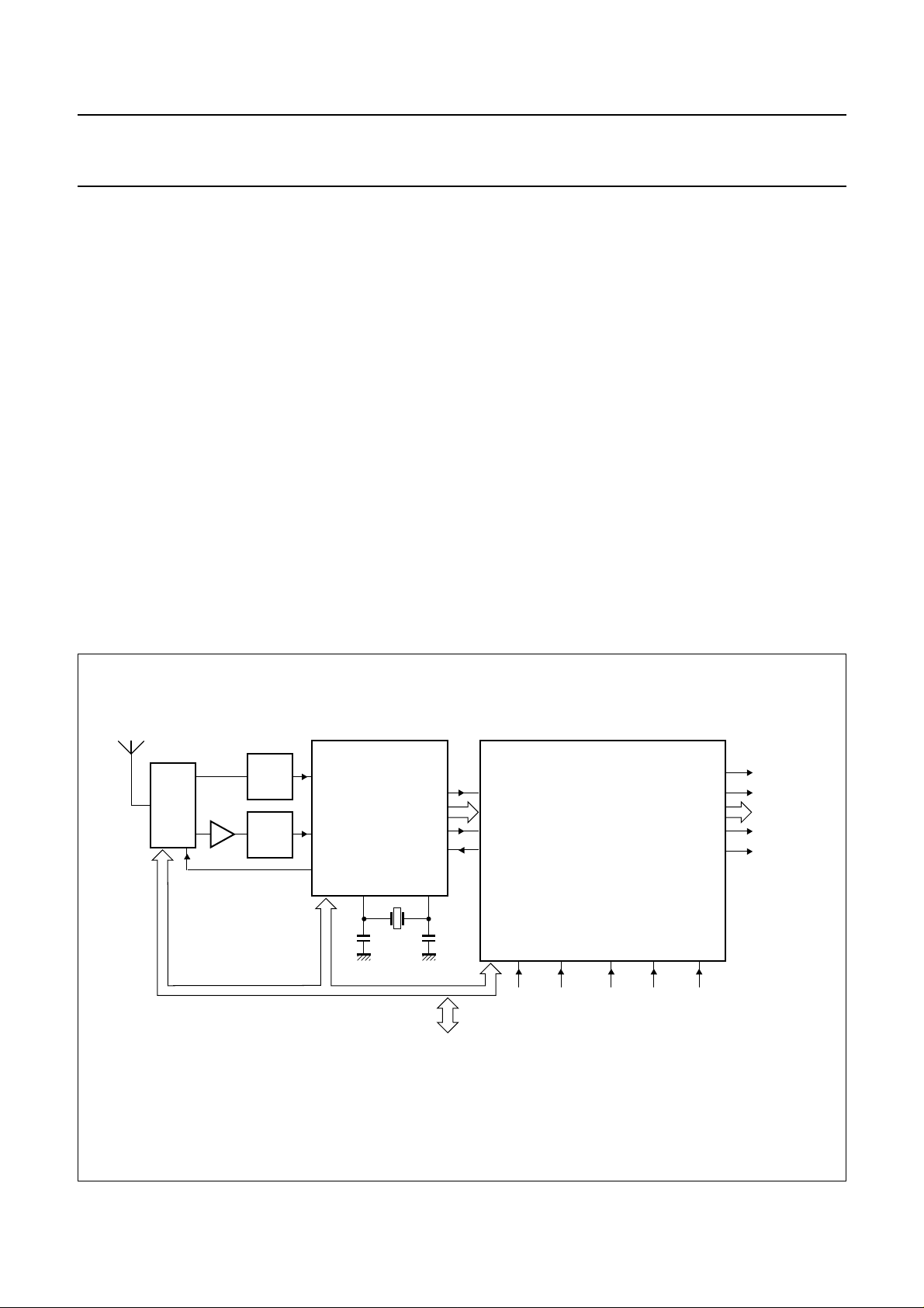
An application using the TDA8961 and the TDA8980
NTSC/ATSC TV input processor for TV and Multi-Media is
shown in Fig.1. A tuner converts the incoming RF signal to
a fixed IF centered at 44 MHz. The output signal from the
tunerisfilteredandfedtotheTDA8980whichperformsthe
following functions:
• Decodes the analog NTSC signals: The audio signals
aredigitized,using on-chip audio stereo A/D converters,
intoanI2S-busstream;thevideoinformationisdigitized,
using on-chip video A/D converters, into an ITU656
stream.
TDA8961
• Down converts the incoming 6 MHz wide 8-VSB IF
signal to a low-IF signal centered at 4 MHz: The low-IF
signal is then digitized, using an on-chip 10-bit A/D
converter, and fed to the TDA8961 for further
processing. In this application, AGC is also managed by
the TDA8980 so that no other external components,
such as an operational amplifier loop integrator, are
required.
Although the TDA8980 has an internal 2-D comb filter,
external filters such as a 3-D comb filter and other picture
improvementdevices can easily be connected. Soundcan
be decoded using an external device such as the
TDA9851 I2C-bus controlled economic BTSC stereo
decoder. This IC has an internal switch allowing it to
process either analog NTSC IF or digital 8-VSB IF signals.
A12 MHzclocksignal is generated using a 12 MHz crystal
connected to the TDA8980. The TDA8961 also uses this
clocksignal which is fed from theTDA8980to pin XTALI of
the TDA8961.
handbook, full pagewidth
TUNER
2
I
C
NTSC
SAW
FILTER
FLAT
SAW
FILTER
TDA8980
TVIFIN
VSBIFIN
TUNERAGC
2
I
C
X12MOUT
D9 to D0
REF12M
12 MHz
VCLK
VIFAGC
X12MIN
I2C
master
ADCLK
ADIN9 to ADIN0
XTALI
AGCOUT
2
PDI0 PDISYNC PDIVAL
I
C
TDA8961
PDOVAL
PDOERR
PDO7 to PDO0
PDOSYNC
PDOCLK
PDICLK PDIERR
serial MPEG-2 transport
stream input
Fig.1 Front-end design for a hybrid TV system using the TDA8980 and TDA8961.
MPEG-2
transport
stream
MGU085
2000 May 19 3
Page 4
Philips Semiconductors Objective specification
ATSC Digital Terrestrial TV
demodulator/decoder
The incoming data has a sample rate of 36 MHz. This is
internally converted to a sample rate of 21.52 MHz which
is twice the 8-VSB symbol rate. This patented Philips
Semiconductors’ technology eliminates the need for
external symbol timing recovery loop components. When
theTDA8980 is decoding analog NTSC,the TDA8961 can
be set to a ITU656 bypass mode which allows the 8-bit
ITU656 data output from the TDA8980 to appear at the
TDA8961 Moving Pictures Expert Group (MPEG-2)
transport stream output, from where it can be fed to the
main graphics display device in the system.
The recovery of the carrier is performed entirely within the
TDA8961. This function consists of a digital frequency and
Frequency Phase-Locked Loop (FPLL).
Data shaping is performed by a square-root raised-cosine
(half Nyquist) filter having a roll-off factor of 11.5%.
After the TDA8961 has performed carrier recovery,
Nyquist filtering and symbol timing recovery, it then
performs adaptive equalization. The adaptive equalizer
usesaDFEstructurewithequalizationbasedontheATSC
field sync (trained equalization) and/or the 8-VSB data
itself (blind equalization).
The equalizer is followed by a patented NTSC co-channel
interference filter which removes any unwanted NTSC
signal interference from the 8-VSB terrestrial DTV signal.
After trellis decoding, the stream is de-interleaved to a
depth of 52 by a convolutional de-interleaver whose
memory is provided on-chip. The Reed Solomon decoder
is ATSC-compliant, with a length of 207, and able to
TDA8961
correct up to 10 bytes. The decoded stream is then
de-randomized using a pseudo-random binary sequence
(PRBS) and the data passed to a FIFO which prevents the
appearance of irregular gaps in the output data.
The output of the TDA8961 is a clock signal and an
ATSC-compliant MPEG-2 packetized data stream. Signal
flag outputs are provided to indicate the occurrence of
sync bytes, valid data bytes and uncorrected Reed
Solomon blocks. The packetized data stream is available
in either an 8-bit parallel, or a 1-bit serial format for
connection to an MPEG-2 transport stream demultiplexer.
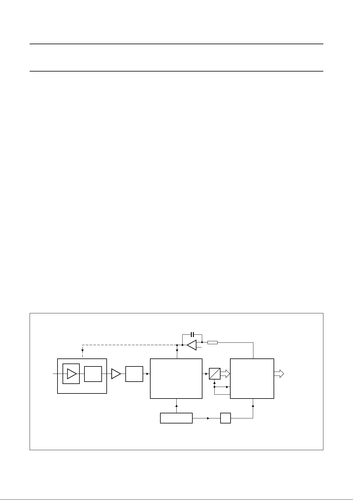
An application using the TDA8961 and a stand-alone
TDA9829 Downconverter for DVB (Digital Video
Broadcast)withanA/DconverterisshowninFig.2.Atuner
converts the incoming RF signal to a fixed IF centered at
44 MHz. The output signal from the tuner is filtered using
two Surface Acoustical Wave (SAW) filters and then down
converted to an IF of 4 MHz by the TDA9829. The signal
is then digitized by an A/D converter at a sample rate of
36 MHz using the clock signal output from the TDA8961.
The full input range of the A/D converter is utilized by
placing it within what is effectively a fine-AGC loop
integrator circuit which has a variable gain stage at the
output of the IF downmixer section. However, it is also
possible to apply the AGC control output of the TDA8961
to the tuner via the integrator. The peak level of the input
signals to the TDA8961 is determined by the AGC output
detector which is located just after the A/D.
V
AGC
TDA9829
VCO
96 MHz
integrator
V
oDVB
AGC
V
ref
AGCOUT
A
ADIN9 to
ADIN0
D
ADCLK
CLK36
÷8
PDO7 to
PDO0
TDA8961
XTALI
12 MHz
MPEG-2
transport
stream
MGU086
handbook, full pagewidth
RF
FILTER
TUNER RF
SAW
44 MHz
SAW
FILTER
V
iIF
IF DOWNMIXER
OSCILLATOR
Fig.2 Front-end design for the TDA8961 using a stand-alone IF down converter (TDA9829) and A/D converter.
2000 May 19 4
Page 5

Philips Semiconductors Objective specification
ATSC Digital Terrestrial TV
TDA8961
demodulator/decoder
QUICK REFERENCE DATA
SYMBOL PARAMETER CONDITIONS MIN. TYP. MAX. UNIT
V
DD
I
DD
f
clk
f
sym
f
s
f
c(IF2)
IL implementation loss −−−dB
α
ro
t
acq
T
amb
P
tot
Note
1. Corresponds to 12 training sequences.
supply voltage 2.7 3.3 3.6 V
supply current VDD= 3.3 V − 390 − mA
clock frequency − 12 − MHz
symbol frequency − 10.76 − Msymbols/s
sample frequency − 36 − MHz
second IF centre frequency − 4 − MHz
half Nyquist filter roll-off factor − 11.5 − %
acquisition time note 1 −−290 ms
ambient temperature −20 − +70 °C
total power dissipation − 1.3 − W
2000 May 19 5
Page 6
Philips Semiconductors Objective specification
ATSC Digital Terrestrial TV
demodulator/decoder
BLOCK DIAGRAM
handbook, full pagewidth
TDI
TCK
20
23
19
22
21
78
79
77
TMS
TDO
TRST
LOCKINDIC
EQLOCKINDIC
RST_AN
BOUNDARY
SCAN TEST
CONTROLLER
CONTROL
ADIN9 TO ADIN0 ADCLK
10, 9, 8, 7, 6,
5, 4, 3, 2, 1
DIGITAL FRONT-END:
SAMPLE RATE CONVERTER
*
FINE AGC
*
CARRIER RECOVERY
*
HALF NYQUIST FILTERING
*
SYNC RECOVERY AND PILOT REMOVAL
*
SYMBOL TIMING RECOVERY
*
ADAPTIVE EQUALIZATION
*
NTSC CO-CHANNEL INTERFACE FILTER
80
TDA8961
66
AGCOUT
A0
A1
SCL
SDA
XT ALI
XT ALO
CLK36
PDISYNC
PDICLK
PDIERR
PDIVAL
PDI0
13
14
15
16
69
70
75
26
30
32
28
27
34
FSYNC
I2C-BUS
INTERFACE
CLOCK
GENERATION
TDA8961
35
FSHNDSHK
SSYNC
67
TRELLIS DECODER
DE-INTERLEAVER
REED SOLOMON DECODER
DE-RANDOMIZER
OUTPUT FORMATTER
39 40
PDOSYNC
PDOV AL PDOERR
PDO7 TO PDO0
43, 44, 45,
47, 48, 49,
51, 52
37 41
PDOCLK
MGU087
Fig.3 Block diagram.
2000 May 19 6
Page 7

Philips Semiconductors Objective specification
ATSC Digital Terrestrial TV
TDA8961
demodulator/decoder
PINNING
SYMBOL PIN I/O DESCRIPTION
ADIN0 1 I data input bit 0 (LSB)
ADIN1 2 I data input bit 1
ADIN2 3 I data input bit 2
ADIN3 4 I data input bit 3
ADIN4 5 I data input bit 4
ADIN5 6 I data input bit 5
ADIN6 7 I data input bit 6
ADIN7 8 I data input bit 7
ADIN8 9 I data input bit 8
ADIN9 10 I data input bit 9 (MSB)
V
DDD1
V
SSD1
A0 13 I I
A1 14 I I
SCL 15 I I
SDA 16 I/O I
V
DDD2
V
SSD2
TDI 19 I TAP controller data input; note 1
TMS 20 I TAP controller test mode select; note 1
TCK 21 I TAP controller test clock; note 1
TRST 22 I TAP controller asynchronous reset (active LOW); notes 1 and 2
TDO 23 O TAP controller test data (3-state); note 1
V
DDD3
V
SSD3
PDISYNC 26 I transport stream interface packet sync indicator
PDI0 27 I transport stream interface packet data bit 0
PDIVAL 28 I transport stream interface packet data valid signal
V
DDD4
PDICLK 30 I transport stream interface packet data clock signal
V
SSD4
PDIERR 32 I transport stream interface packet error signal
V
DDD5
FSYNC 34 I field sync strobe (for debug modes)
SSYNC 35 I segment sync strobe (for debug modes)
V
SSD5
PDOERR 37 O transport stream interface packet error signal (3-state)
V
DDQ1
PDOSYNC 39 O transport stream interface packet sync indicator signal (3-state)
PDOVAL 40 O transport stream interface packet data valid indicator signal (3-state)
11 − digital core supply voltage 1 (3.3 V)
12 − digital core ground 1
2
C-bus slave address bit 0
2
C-bus slave address bit 1
2
C-bus clock
2
C-bus serial data
17 − I/O supply (3.3 V)
18 − digital core ground 2
24 − digital core supply voltage 3 (3.3 V)
25 − digital core ground 3
29 − digital core supply voltage 4 (3.3 V)
31 − digital core ground 4
33 − digital core supply voltage 5 (3.3 V)
36 − digital core ground 5
38 − I/O supply voltage 1 (3.3 V)
2000 May 19 7
Page 8

Philips Semiconductors Objective specification
ATSC Digital Terrestrial TV
TDA8961
demodulator/decoder
SYMBOL PIN I/O DESCRIPTION
PDOCLK 41 O transport stream interface packet data clock signal (3-state)
V
SSQ1
PDO7 43 O transport stream interface packet data bit 7 (3-state)
PDO6 44 O transport stream interface packet data bit 6 (3-state)
PDO5 45 O transport stream interface packet data bit 5 (3-state)
V
DDQ2
PDO4 47 O transport stream interface packet data bit 4 (3-state)
PDO3 48 O transport stream interface packet data bit 3 (3-state)
PDO2 49 O transport stream interface packet data bit 2 (3-state)
V
SSQ2
PDO1 51 O transport stream interface packet data bit 1(3-state)
PDO0 52 O transport stream interface packet data bit 0 (3-state)
V
DDQ3
n.c. 54 not connected
n.c. 55 not connected
V
SSQ3
n.c. 57 not connected
n.c. 58 not connected
n.c. 59 not connected
V
DDQ4
n.c. 61 not connected
n.c. 62 not connected
n.c. 63 not connected
V
SSQ4
n.c. 65 not connected
AGCOUT 66 O AGC control (3-state)
FSHNDSHK 67 O field sync strobe or symbol capture memory handshake signal
V
DDA1
XTALI 69 I external crystal
XTALO 70 O external crystal
V
SSA1
V
DDA2
n.c. 73 not connected
V
DDQ5
CLK36 75 O 36 MHz clock signal
V
SSQ5
RST_AN 77 I asynchronous reset (active LOW)
LOCKINDIC 78 O front-end lock indicator
EQLOCKINDIC 79 O equalizer lock indicator
ADCLK 80 I incoming data sampling clock signal (36 MHz)
42 − I/O ground 1
46 − I/O supply voltage 2 (3.3 V)
50 − I/O ground 2
53 − I/O supply 3 (3.3 V)
56 − I/O ground 3
60 − I/O supply 4 (3.3 V)
64 − I/O ground 4
68 − analog supply voltage (3.3 V)
71 − analog ground 1
72 − analog supply 2 (3.3 V)
74 − I/O supply 5 (3.3 V)
76 − I/O ground 5
2000 May 19 8
Page 9

Philips Semiconductors Objective specification
ATSC Digital Terrestrial TV
TDA8961
demodulator/decoder
Notes
1. Input pins TCK, TDI, TMS and TRST have an internal pull-up transistor and must be connected to ground when not
used; pin TDO is a 3-state output in accordance with IEEE 1149.1.
2. Pin TRST is active LOW. It can be used to immediately force the Test Access Port (TAP) controller to the test logic
reset state (normal operation) in accordance with IEEE 1149.1.
2000 May 19 9
Page 10

Philips Semiconductors Objective specification
ATSC Digital Terrestrial TV
demodulator/decoder
ADCLK
handbook, full pagewidth
ADIN0
ADIN1
ADIN2
ADIN3
ADIN4
ADIN5
ADIN6
ADIN7
ADIN8
ADIN9
V
DDD1
V
SSD1
SDA
V
DDD2
V
SSD2
TMS
TCK
TRST
TDO
V
DDD3
A0
A1
SCL
TDI
1
2
3
4
5
6
7
8
9
10
11
12
13
14
15
16
17
18
19
20
21
22
23
24
EQLOCKINDIC
80
79
25
26
LOCKINDIC
RST_AN
78
77
27
28
SSQ5
V
76
29
CLK36
75
30
DDQ5
V
n.c.
74
73
TDA8961
31
32
DDA2VSSA1
V
72
71
33
34
XTALO
70
35
XTALI
69
36
DDA1
V
68
37
FSHNDSHK
AGCOUT
67
66
38
39
n.c.
65
40
64
63
62
61
60
59
58
57
56
55
54
53
52
51
50
49
48
47
46
45
44
43
42
41
MGU088
TDA8961
V
SSQ4
n.c.
n.c.
n.c.
V
DDQ4
n.c.
n.c.
n.c.
V
SSQ3
n.c.
n.c.
V
DDQ3
PDO0
PDO1
V
SSQ2
PDO2
PDO3
PDO4
V
DDQ2
PDO5
PDO6
PDO7
V
SSQ1
PDOCLK
SSD3
V
PDI0
PDISYNC
V
PDIVAL
DDD4
V
PDICLK
SSD4
PDIERR
Fig.4 Pin configuration.
2000 May 19 10
DDD5
V
FSYNC
SSYNC
SSD5
V
DDQ1
V
PDOERR
PDOVAL
PDOSYNC
Page 11

Philips Semiconductors Objective specification
ATSC Digital Terrestrial TV
demodulator/decoder
FUNCTIONAL DESCRIPTION
The internal architecture of the TDA8961 basically
comprises two parts:
• The front-end: containing the AGC, carrier recovery,
halfNyquistfilter,symboltimingrecovery,syncrecovery
and adaptive equalization sections.
• The back-end: containing the NTSC co-channel
rejection filter, trellis decoder, de-interleaver, the Reed
Solomon decoder and de-randomizer sections.
Sample rate converter
INTRODUCTION
The sample rate converter section changes the incoming
data frequency of 36 MHz to an internal sampling
frequency of twice the symbol rate.
The 10-bit wide data from either the TDA8980 or a
stand-alone A/D converter (TDA8763A is recommended)
arrives at the sample rate converter input of the TDA8961
via inputs ADIN9 to ADIN0. The format of the incoming
samples can be programmed by the status of I2C-bus
bit AD_FMT (see Table 9). The format can be either two’s
complement or binary. The default setting is binary to
comply with the TDA8980.
TDA8961
Fine AGC
The fine AGC section controls the gain of analog signals
over a range of ±20 dB.
The level of the signal at pins ADIN9 to ADIN0 is
monitored and an average level from several samples is
acquired. The default number of samples is 64, but this
value can be set to 256 by setting I2C-bus
bit AGC_SAMPLES (see Table 10). A comparator
compares the level of the filtered signal with a threshold
level represented by a signed four-bit value set by I2C-bus
bits AGC_TR_LOW. The comparator output determines
the level at pin AGCOUT which is used to either charge or
discharge an off-chip ideal integrator, which in turn,
controls the gain of the tuner front-end module.
To make the level at pin AGCOUT compatible with the
AGC circuits in other devices, the comparator output can
be inverted by setting I2C-bus bit AGC_DIR (see
Table 10). The default value of bit AGC_DIR is 0 making
theoutput at pin AGCOUT compatible with the AGC circuit
in the TDA8980. The levels at pin AGCOUT with respect
to the value of bit AGC_DIR are shown in Table 2.
The AGC section can be reset by setting I2C-bus
bit AGC_RESET (see Table 8).
PINNING
The functions of the input interface pins are given in
Table 1.If a stand-alone A/D converteris used, pin CLK36
is connected externally to pin ADCLK.
Table 1 Input interface
NAME FUNCTION
ADIN9 to ADIN0 10-bit data input (from external A/D converter)
ADCLK 36 MHz clock signal input
CLK36 clock signal output for sampling incoming data (to external A/D converter)
Table 2 AGC
2
I
FILTER OUTPUT LEVEL COMPARATOR OUTPUT
Above threshold 1 0 1
Below threshold 0 0 0
Above threshold 1 1 0
Below threshold 0 1 1
Equal to threshold Z 0 Z
C-bus
bit AGC_DIR
Pin AGCOUT
2000 May 19 11
Page 12

Philips Semiconductors Objective specification
ATSC Digital Terrestrial TV
demodulator/decoder
Carrier recovery
The carrier recovery circuit recovers the frequency and
phase of the pilot carrier signal. If, as in some cases, the
pilot signal is present at the higher edge of the VSB
spectrum, the I2C-bus bit CR_INV can be set to ensure
that when the frequency is shifted, the pilot signal is DC.
Half Nyquist filtering
The half Nyquist filtering section is a square-root
raised-cosine filter with 11.5% roll-off.
Sync recovery
The sync recovery section performs several functions
including the recovery of segment sync and field sync.
When this section detects the data segment sync signal,
pin LOCKINDIC goes HIGH. The status of
pin LOCKINDIC can also be read via the I2C-bus
bit LOCK_INDICATOR (see Table 16).
TDA8961
CONTROL
An integrated sophisticated finite state machine controls
the sequence of operations that must be performed to
correctly decode a valid VSB data signal into an MPEG-2
packetized transport stream.
After a reset has been applied, the finite state machine is
in state 0. When a valid VSB data signal is detected, the
finite state machine ensures that the following three states
occur.
State 1: channel acquisition
In this state there is either no channel signal present or a
channel signal is in the process of being acquired. Before
the channel signal can be acquired, the AGC, timing
recovery and carrier recovery loops must first lock onto it.
If segment sync lock is lost, either pin LOCKINDIC goes
LOW, or a hardware reset is applied to the TDA8961 and
the finite state machine returns to state 0.
Timing recovery
The timing recovery section takes signals from the half
Nyquist filter and forms part of a closed loop in order to
acquire and maintain a constant sampling rate and clock
frequency for the complete system.
Adaptive equalizer
The adaptive equalizer comprises a forward filter and a
feedback filter section. At every symbol period, it receives
demodulated symbols from the sync recovery section.
The equalizer filters these symbols in an attempt to
eliminate the effects of multipath conditions on the symbol
stream during transmission. The coefficients of the filters
are updated every symbol period using the training
sequence and/or using blind equalization if required.
The equalizer is designed to correct a maximum pre-echo
of 2.32 µs and a maximum post-echo of 22.5 µs.
The equalizer has an optimized typical acquisition time of
12 training sequences, which corresponds to about
290 ms. It is defined that acquisition occurs when the
output signal-to-noise ratio reaches the Threshold Of
Visibility (TOV). For 8-VSB, the ATSC defines a TOV of
14.9 dB.
A Mean Square Error (MSE) signal is generated based on
the training signal and on the output of the equalizer.
The errorsignal represents a 16-bit value which isreadvia
the I2C-bus bit MSE (see Table 18) and used to monitor
the channel adaptation process.
It is possible to use software control to extend the range of
the feedback filter to a maximum of 80 µs.
State 2: equalizer training
The finite state machine remains in state 1 until the MSE
of the equalized training sequence falls between two
specificthreshold values. It should be noted thatinstate 1,
theback-end section of the TDA8961is continuously reset
to make sure that after its demodulator has locked onto a
signal, the trellis decoder and the following sections begin
processing at the start of the next complete data field.
The value of I2C-bus bit MSE can be used for applications
such as antenna pointing.
State 3: normal operation
Normallythe finite state machine remainsin state 2 unless
asynchronization error occurs. If the MSE oftheequalized
training sequence exceeds 100 ms, the equalizer is reset
for one symbol period and the adaptation process restarts.
If the demodulator synchronization and equalization are
both locked, pin EQLOCKINDIC goes HIGH and I2C-bus
bit LOCK_INDICATOR is set to 11 (see Table 16).
The filtered output signal is then routed to the NTSC
co-channel interference filter.
NTSC co-channel interference filter
The NTSC co-channel interference filter uses patented
Philips’ technology making its performance considerably
better than the ATSC specified comb filter. The filter can
be bypassed by setting I2C-bus bit FLT_BYPASS (see
Table 13).
2000 May 19 12
Page 13

Philips Semiconductors Objective specification
ATSC Digital Terrestrial TV
demodulator/decoder
Transport stream interface
INTRODUCTION
The transport stream interface performs the following
functions:
• Buffers the data from the Reed Solomon decoder and
de-randomizer section
• Inserts the MPEG sync byte at the start of every packet
• Indicates error conditions using a
transport_error_indicator bit in the packet header and
the error signal output PDOERR.
• Outputs either a serial or a parallel output format.
PINNING
The functions of the transport stream interface outputs are
summarized in Table 3. It should be noted that different
source decoder devices may have different uses for the
PDOERR output; its polarity is programmable using
I2C-bus bit FPBP (see Table 14).
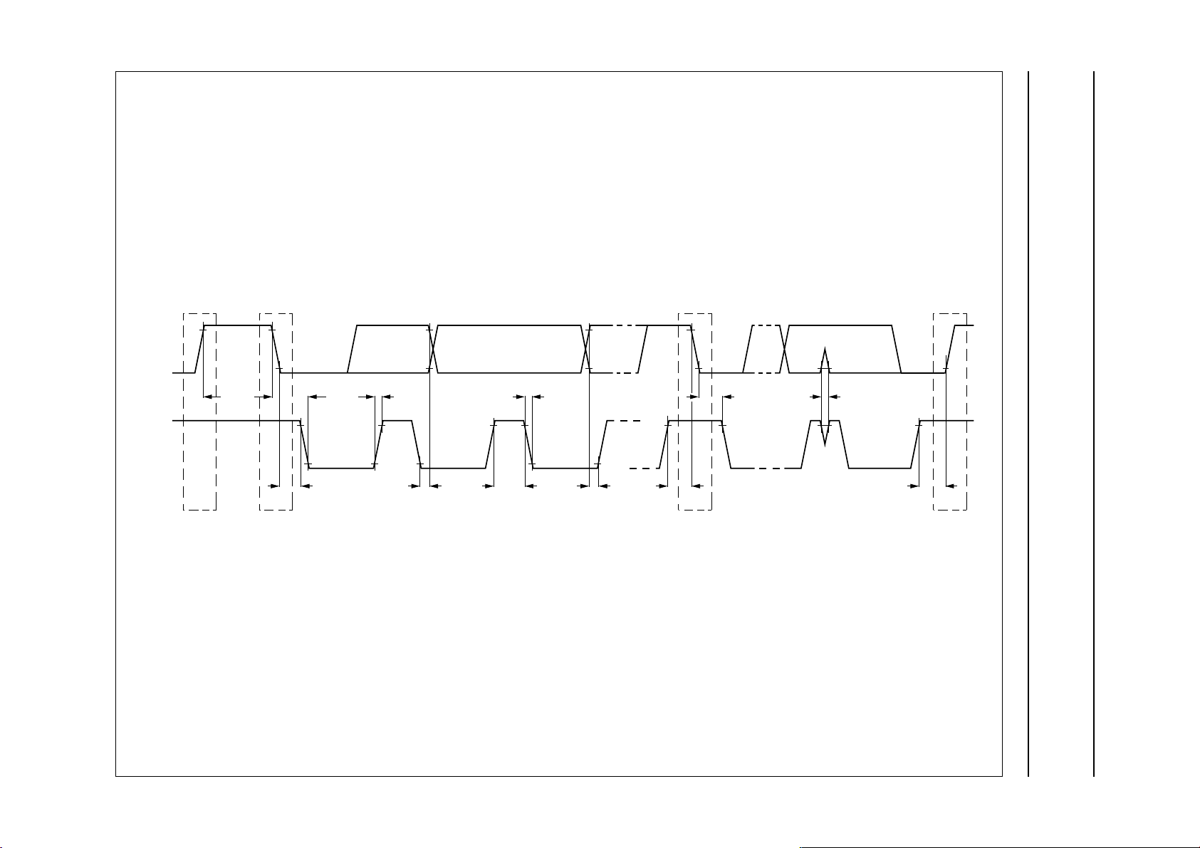
PARALLEL OUTPUT FORMAT
Figure 5 shows the timing diagram for the parallel output
format. The PDOSYNC signal indicates the occurrence of
the sync byte in the packet and is only HIGH for one clock
period. The polarity of the PDOVAL and PDOERR signals
is programmable via I2C-bus bits FDVP and FPBP
respectively; Fig.5 shows their default polarities.
The PDOVAL signal is active for the duration of the
188 bytes of the transport stream packet. When the
188 bytes have been transferred, the PDOVAL signal
goes LOW for at least ten PDOCLK cycles during which,
TDA8961
when used with DVB devices, the parity bytes are
transferred; when used with non-DVB devices, zeroed
parity bytes and field sync data are transferred.
The period when the PDOVAL signal is LOWcan vary, but
will be a minimum of ten PDOCLK cycles. Due to the
averaging operation of the FIFO, the number of parity
bytes transferred can vary slightly. The PDOCLK signal
runs continuously and is not affected by a reset. In parallel
output format, it has a frequency of 3 MHz.
When the TDA8961 is trying to acquire a channel, the
PDOERR signal goes HIGH (I2C-bus bit FPBP = 1). If this
occurs, the PDOVAL signal stays LOW.
SERIAL OUTPUT FORMAT
Figure 6 shows the timing diagram for the serial output
format. The LSB of the 8-bit PDO data bus is used to
output the MPEG-2 transport stream packets.
The PDOSYNC signal indicates the occurrence of the
sync byte in the packet and is only HIGH during
8 PDOCLK cycles. The polarity of the PDOVAL and
PDOERR signals is programmable via I2C-bus bits FDVP
and FPBP respectively; Fig.6 shows their default
polarities.
The PDOVAL signal is active for the duration of the
188 bytes of the transport stream packet. When the
188 bytes have been transferred, the PDOVAL signal
goesLOWforaperiodcorrespondingtotheduration of the
parity and field sync information. Figure 6 shows the
PDOERR signal is HIGH for the whole packet length
indicating that the packet contains errors. The PDOCLK
signal has a frequency of 27 MHz.
Table 3 Transport stream interface outputs
All pins are 3-state outputs.
SYMBOL FUNCTION
PDOCLK clock signal for MPEG-2 packet data bytes (parallel and serial)
PDOVAL indicates a valid data signal
PDO7 to PDO0 packet data bits 7 to 0 (8-bit wide output bus)
PDOSYNC indicates the start of a packet; goes HIGH at the start of a packet and stays HIGH during the first
byte, otherwise known as the sync byte
PDOERR indicatespacket error; goes HIGH (I
Reed Solomon decoder found more errors than it could correct
Note
1. In serial output format, only pin PDO0 (LSB) is used to output the data.
2000 May 19 13
2
C-bus bit FPBP = 1) for every packet (188 bytes) in which the
(1)
Page 14

Philips Semiconductors Objective specification
ATSC Digital Terrestrial TV
demodulator/decoder
handbook, full pagewidth
PDOCLK
PDO7 to
PDO0
PDOSYNC
PDOVAL
PDOERR
(1)
20
1 2 186 187
(3)
(3)
(2) (2) (2) (2) (1)
TDA8961
1
MGU090
(1) Sync byte.
(2) Parity byte; contents set to 00H.
(3) The polarity of these signals is programmable.
handbook, full pagewidth
PDOCLK
MSB
PDO0
PDOSYNC
PDOVAL
PDOERR
65
(1)
(2)
(2)
sync byte (47H) byte 1 byte 187
Fig.5 Parallel output format.
LSB
76 07
0
76
0
7
0
MGU091
(1) Sync byte.
(2) The polarity of these signals is programmable.
Fig.6 Serial output format.
2000 May 19 14
Page 15

Philips Semiconductors Objective specification
ATSC Digital Terrestrial TV
demodulator/decoder
SYNC BYTE AND TRANSPORT STREAM ERROR INDICATOR
Figure 7 shows the structure of the so-called transport
stream packet header of which only the first two bytes are
significantto the TDA8961. The first byte in each headeris
the sync byte which must have the same value for all
packets in accordance with the MPEG-2 standard
specification. The TDA8961 sets the sync byte for each
outgoing transport stream packet to 47H. The MSB of the
second byte in the header is the
transport_error_indicator bit. It is asserted when the Reed
Solomon decoder is unable to correct all errors in the
transport stream packet and indicates that the packet
contains invalid data.
To perform bit error rate (BER) measurements, the
external channel decoder generates a pseudo-random bit
sequence (PRBS) in the last 187 bytes of each transport
stream packet.The same PRBS signal is generated within
the BER tester which compares it with the PRBS in each
transport packet and records any mismatch as an error.
It should be noted that during BER measurements, the
TDA8961 must not be allowed to set the
transport_error_indicator bit. This option is possible using
I2C-bus bit FTEI (see Table 14). If bit FTEI is not set, the
transport error interface bit is not allowed to indicate an
error. If bit FTEI is set, the Reed Solomon decoder is
allowed to set the transport_error_indicator bit according
to the result of the error correction process. This is the
default setting.
TDA8961
SERIAL TRANSPORT STREAM INPUT
The TDA8961 can be used with another channel decoder
without requiring the transport stream outputs from either
decoder to be selected by an external switch. This
configuration requires the serial transport stream output
from the other channel decoder to be connected to the
serial transport stream input of the TDA8961. When the
system requires the transport stream from the other
channel decoder, the TDA8961 internally connects
PDIERR to PDOERR, PDIVAL to PDOVAL, PDICLK to
PDOCLK, PDISYNC to PDOSYNC and PDI0 to PDO0
allowing the transport stream from the other channel
decoder to pass through the TDA8961. This pass-through
mode is enabled by setting the value of I2C-bus TSMODE
bits to 11 (see Table 14).
ITU656 BYPASS MODE
Figure 1 shows the tuner output connected to the
TDA8980whichprocessestheIFandthenoutputsan8-bit
wide MPEG-2 transport stream to the TDA8961 where it is
furtherprocessedbeforeitisoutputto the video processor.
This arrangement allows one system to receive both
analog and digital broadcasts. When analog signals are
received, the TDA8980 supplies an ITU656 format video
stream to the TDA8961 input interface comprising
pins ADIN9 to ADIN0 and ADCLK. The ITU656 format
uses 8-bit data and a 27 MHz clock signal.
handbook, full pagewidth
adaptation field
(if present)
sync byte
transport_error_indicator
188 bytes
transport packet header
00
1 0 0 0 1 1 1
MSB
Fig.7 Transport packet header structure.
2000 May 19 15
payload
(if present)
1st byte
4th byte
LSB
MGR605
Page 16

Philips Semiconductors Objective specification
ATSC Digital Terrestrial TV
demodulator/decoder
Pins PDO0 to PDO7andPDOCLKarenormallypart of the
transport stream output interface. The signals to these
pins are normally routed via an internal multiplexer.
However, in the ITU656 bypass mode, these pins connect
directly to the lower 8 bits of ADIN9 to ADIN0 and ADCLK.
In this mode, PDOSYNC and PDOVAL are kept LOW and
the polarity of PDOERR depends on the setting of I2C-bus
bit FPBP. If required, these transport stream interface
outputs can be forced to 3-state mode by making I2C-bus
bit TSO = 0 (see Table 14).
ITU656 bypass mode is enabled by setting the
I2C-bus TSMODE bits to 10.
SEGMENT ERROR COUNTER
The TDA8961 transport stream output interface is able to
calculate the Segment Error, or packet error, Rate (SER)
over a certain time period. The time period can be set to
either 1, 4, 8 or 16 seconds by the I2C-bus bits SERTM
(see Table 14). The IC counts any packet errors occurring
in the set time period. At the end of the time period, the
16-bit value representing the counted number of packet
errors can be read via I2C-bus bit SER (see Table 19).
After a reset, the register value is set to 12935 (3287H)
which is equivalent to an infinite SER. The TDA8961 is
able to automatically reset itself when the SER exceeds a
presetthresholdvalue.TheSERthresholdis a 14-bit value
programmable in the range 3 to 13000 represented by
I2C-bus bits SER_THRES (see Table 14).
TDA8961
EXTERNAL INTERFACE
The TAP external interface has five pins whose functions
are described in Table 4.
Table 4 TAP external interface
SIGNAL DESCRIPTION
TMS Test mode select input
TCK Test clock signal input
TDI Test data input
TDO Test data output
TRST Test asynchronous reset input
2
I
C-bus interface
The I2C-bus interface writes control information to, and
reads low-speed diagnostic information from the
TDA8961. The key features of the I2C-bus interface are:
• I2C-bus data rate of up to 400 kbits/s
• Support for only 7-bit addressing and the ability to
externally modify the slave address.
A typical system using the I2C-bus interface is shown in
Fig.8. The TDA8961 is acting as a slave and is connected
to a master via the I2C-bus lines SCL and SDA. It should
be noted that the SCL and SDA lines are connected to
separate pull-up resistors.
It should be noted that the time period set by the
SERTM bits should be long enough to allow this threshold
to be reached. This reset function is enabled by setting
I2C-busbit SER_RST(seeTable 14).The reset function is
disabled by default.
Boundary scan interface
The TDA8961 TAP conforms to the IEEE 1149.1 (JTAG)
standard.Itisused for board-level testing and for internally
testing integrated circuits. The JTAG standard defines the
on-chip test logic which comprises an instruction register,
a group of test data registers including a bypass register
and a boundary scan register, four dedicated pins
comprising the TAP, and a TAP controller.
2000 May 19 16
handbook, halfpage
I2C-BUS
MASTER
SCL
SDA
Fig.8 Typical I2C system implementation.
TDA8961
V
DD
R
pu
R
pu
MGU089
Page 17

Philips Semiconductors Objective specification
ATSC Digital Terrestrial TV
demodulator/decoder
EXTERNAL INTERFACE
The I2C-bus external interface has three pins whose
functions are described in Table 5.
2
Table 5 I
SDA I
SCL I
A0 I
A1 I
The TDA8961 I/O and I2C-bus signals range between
ground and 3.3 V. Systems that have devices which
operate at different supply voltages may require special
circuitry to allow these devices to communicate and to be
controlled. Circuit requirements are described in
“Application Report AN97055”
available from Philips Semiconductors.
ADDRESSING THE DEVICE
The TDA8961 must be addressed by its 7-bit (A6-A0)
slave address sent via the system I2C-bus in accordance
with the correct protocols, and with bit R/W set to either 1
(write data) or 0 (read data).
C-bus external interface
SIGNAL DESCRIPTION
2
C-bus serial data input/output
2
C-bus clock input
2
C-bus slave address input bit 0
2
C-bus slave address input bit 1
(issued Aug. 04, 1997)
TDA8961
A write operation is shown in Fig.9. Themaster transmitter
sends a START condition followed by the 7-bit slave
address which is followed by bit R/
receiver (TDA8961) responds by sending an
acknowledge.Themaster then sends write data starting at
address zero. If the master sends more than one byte of
write data, the TDA8961 automatically increments to the
next address. The TDA8961 sends an acknowledge after
it receives each byte. If the TDA8961 does not
acknowledge the data transfer and/or the master sends a
STOPcondition,thedata transfer stops. It should be noted
that the TDA8961 does not support I2C-bus
sub-addressing. Therefore, each I2C-bus transfer starting
with the transmission of the slave address and bit R/W,
starts at address zero.
A read operation is shown in Fig.10. The master
transmitter sends a START condition followed by the 7-bit
slave address which is followed by bit R/W set to 1.
The slave receiver (TDA8961) responds by sending an
acknowledge and the value at address zero. The master
responds by sending an acknowledge. If the master
follows the acknowledge with a STOP condition, the data
transfer stops, otherwise the slave is allowed to transfer
more bytes. The slave TDA8961 automatically increments
to the next address of read data to be sent to the master.
W set to 0. The slave
The slave address of the TDA8961 is given in Table 6.
Bits A6 to A2 are preset, but bits A1 and A0 can be set via
their corresponding external pins.
Table 6 TDA8961 slave address
A6 A5 A4 A3 A2 A1 A0 R/W
00011A1A00=write
1 = read
2000 May 19 17
Page 18

Philips Semiconductors Objective specification
ATSC Digital Terrestrial TV
demodulator/decoder
handbook, full pagewidth
(1) From master to slave
(2) S = START condition
(3) Logic 0 (write)
(4) From slave to master
(1)(2) (1)(3) (4)(5) (1) (4)(5) (4)(5)(6)(1) (1)(7)(1)
S A DATA A
R/W A/A
(5) A = acknowledge (SDA LOW)
(6) A = not acknowledge (SDA HIGH)
(7) P = STOP condition
(8) Data transferred (n bytes + acknowledge).
DATA PSLAVE ADDRESS
(8)
TDA8961
MGR607
Fig.9 Master transmitter addressing a slave receiver with a 7-bit address (write mode).
handbook, full pagewidth
(1) From master to slave.
(2) S = START condition.
(3) Logic 1 (read).
(4) From slave to master.
(5) A = acknowledge (SDA LOW).
(1)(2) (1)(3) (4)(5) (4) (1)(5) (1)(6)(4) (1)(7)(1)
S A DATA A
R/W A
(6) A = not acknowledge (SDA HIGH).
(7) P = STOP condition.
(8) Data transferred (n bytes + acknowledge).
DATA PSLAVE ADDRESS
(8)
MGR608
Fig.10 Master transmitter addressing a slave receiver with a 7-bit address (read mode).
2000 May 19 18
Page 19

This text is here in white to force landscape pages to be rotated correctly when browsing through the pdf in the Acrobat reader.This text is here in
_white to force landscape pages to be rotated correctly when browsing through the pdf in the Acrobat reader.This text is here inThis text is here in
white to force landscape pages to be rotated correctly when browsing through the pdf in the Acrobat reader. white to force landscape pages to be ...
2000 May 19 19
2
C-BUS REGISTER MAP
I
2
Table 7 I
C-bus write register overview
Philips Semiconductors Objective specification
ATSC Digital Terrestrial TV
demodulator/decoder
FUNCTION
General
settings
SRC 05 AD_FMT
AGC/
Carrier
recovery
Equalizer 11 MSE_THR_1[15 to 8]
ADDRESS
(HEX)
00 EQ_RST_
01 AGC_RESET CR_RESET TR_RESET SR_RESET
02
03
04
06 AGC_
07 AGC_DIR CR_INV
08
09
0A
0B
0C
0D
0E
0F
10
12 MSE_THR_1[7 to 0]
13 MSE_THR_2[15 to 8]
14 MSE_THR_2[7 to 0]
15
16
17
18
19
1A
D7 D6 D5 D4 D3 D2 D1 D0
EQ_FREEZE EQ_RESET BE_RESET GNRL_RESET INITIAL_
DISABLE
AGC_TR_LOW
SAMPLES
RESET
TDA8961
Page 20

This text is here in white to force landscape pages to be rotated correctly when browsing through the pdf in the Acrobat reader.This text is here in
_white to force landscape pages to be rotated correctly when browsing through the pdf in the Acrobat reader.This text is here inThis text is here in
white to force landscape pages to be rotated correctly when browsing through the pdf in the Acrobat reader. white to force landscape pages to be ...
2000 May 19 20
FUNCTION
NTSC
co-channel
interference
filter
Transport
stream
interface
ADDRESS
(HEX)
1B
1C
1D
1E
1F
20
21
22
23
24
25
26
27
28
29
2A
2B
2C
2D FLT_BYPASS
2E
2F
30 FTEI FPBP FDVP TSO PMSM
31 SER_RST TSMODE SERTM
32 SER_THRES[13 to 8]
32 SER_THRES[7 to 0]
33
34
D7 D6 D5 D4 D3 D2 D1 D0
Philips Semiconductors Objective specification
ATSC Digital Terrestrial TV
demodulator/decoder
TDA8961
Page 21

Philips Semiconductors Objective specification
ATSC Digital Terrestrial TV
demodulator/decoder
Table 8 General settings (write)
BIT NAME BIT VALUE DESCRIPTION
INITIAL_RESET 0 normal operation (default)
1 initial reset; note 1
GNRL_RESET 0 normal operation (default)
1 general reset; note 2
BE_RESET 0 normal operation (default)
1 backend reset
EQ_RESET 0 normal operation (default)
1 equalizer reset
EQ_FREEZE 0 normal operation (default)
1 equalizer adaptation freeze
EQ_RST_DISABLE 0 normal operation (default)
1 equalizer reset disable
FE_RST_DISABLE 0 normal operation (default)
1 front-end reset disable
SR_RESET 0 normal operation (default)
1 reset sync recovery section
AGC_RESET 0 normal operation (default)
1 reset input AGC
TR_RESET 0 normal operation (default)
1 reset the timing recovery
CR_RESET 0 normal operation (default)
1 carrier recovery reset enable
TDA8961
Notes
1. Operating modes and control parameters of all sections in the TDA8961 are not affected.
2. Operating modes and control parameters of all sections in the TDA8961 are reset to their initial values.
Table 9 Sample rate converter settings (write)
BIT NAME BIT VALUE DESCRIPTION
AD_FMT 0 two’s complement
1 binary (default)
Table 10 AGC settings (write)
BIT NAME BIT VALUE DESCRIPTION
AGC_SAMPLES 0 average over 64 samples (default)
1 average over 256 samples
AGC_DIR 0 AGC operation compatible with TDA8980 (default)
1 AGC operation compatible with TDA9819/9829
AGC_TR_LOW − AGC threshold value
2000 May 19 21
Page 22

Philips Semiconductors Objective specification
ATSC Digital Terrestrial TV
demodulator/decoder
Table 11 Carrier recovery settings (write)
BIT NAME BIT VALUE DESCRIPTION
CR_INV 0 selects non-inverted spectrum; carrier at lower band-edge
1 selects inverted spectrum; carrier at higher band-edge (default)
Table 12 Equalizer settings (write)
BIT NAME BIT VALUE DESCRIPTION
MSE_THR_1 − MSE loss-of-convergence threshold value 1
MSE_THR_2 − MSE loss-of-convergence threshold value 2
Table 13 NTSC co-channel interference filter settings (write)
BIT NAME BIT VALUE DESCRIPTION
FLT_BYPASS 0 normal operation (default)
1 bypass NTSC co-channel interference filter
Table 14 Transport stream interface settings (write)
TDA8961
BIT NAME BIT VALUE DESCRIPTION
PMSM 0 parallel format (default)
1 serial format
TSO 0 transport stream outputs in 3-state mode
1 transport stream outputs active (default)
FDVP 0 polarity of PDOVAL is LOW during the packet length of 188 data bytes
1 polarity of PDOVAL is HIGH during the packet length of 188 data bytes
(default)
FPBP 0 polarity of PDOERR goes LOW if block cannot be corrected
1 polarity of PDOERR goes HIGH if block cannot be corrected (default)
FTEI 0 transport_error_indicator bit is not allowed to indicate any errors detected in
the transport stream
1 transport_error_indicator bit is allowed to indicate errors in the transport
stream which could not be corrected by the Reed Solomon decoder (default)
TSMODE 00 normal operation (default)
01 reserved
10 ITU656 bypass mode
11 serialized transport input (pass-through mode)
SERTM 00 SER is calculated over a 1 second period (default)
01 SER is calculated over a 4 second period
10 SER is calculated over a 8 second period
11 SER is calculated over a 16 second period
SER_THRES SER threshold value (used if SER_RST is set to 1)
SER_RST 0 normal operation (default)
1 TDA8961 is reset when the SER exceeds 2.5
2000 May 19 22
Page 23

Philips Semiconductors Objective specification
ATSC Digital Terrestrial TV
demodulator/decoder
Table 15 I2C-bus read registers overview
(1)
ADDRESS
(HEX)
00 LOCK_I
01 CR_OFFSET[7 to 0]
02
03
05 MSE[7 to 0]
06
07
08
09
0A
0B SER[15 to 8]
0C SER[7 to 0]
0D TYPE[3 to 0] VERSION[3 to 0]
D7 D6 D5 D4 D3 D2 D1 D0
FUNCTION
Basic
operation
Carrier
recovery
Equalizer 04 MSE[15 to 8]
Transport
stream
interface
IC version
TDA8961
STATE
NDICAT
OR
Note
1. This register allows the type and version of the TDA8961 to be read by the controlling host. The TYPE[3 to 0] field
contains 1H corresponding to the TDA8961. The VERSION[3 to 0] field contains EH corresponding to the TDA8961
version N1E. Philips Semiconductors reserves the right to change the values in this register for future versions of the
TDA8961.
Table 16 General (read)
BIT NAME BIT VALUE DESCRIPTION
STATE 01 state1 (channel acquisition)
10 state2 (equalizer training)
11 state3 (normal operation)
LOCK_INDICATOR 01 channel acquisition: no synchronization; equalization locked
10 equalizer training: synchronization locked; no equalization
11 normal operation: synchronization locked; equalization locked
Table 17 Carrier recovery (read)
BIT NAME BIT VALUE DESCRIPTION
CR_OFFSET − Carrier recovery offset value
Table 18 Equalizer (read)
BIT NAME BIT VALUE DESCRIPTION
MSE − Equalizer mean square error value
2000 May 19 23
Page 24

Philips Semiconductors Objective specification
ATSC Digital Terrestrial TV
TDA8961
demodulator/decoder
Table 19 Transport stream interface (read)
BIT NAME BIT VALUE DESCRIPTION
SER − segment error rate value
Table 20 TDA8961 version (read)
BIT NAME BIT VALUE DESCRIPTION
TYPE 0001 1H = TDA8961
VERSION 1110 EH = TDA8961 version N1E
LIMITING VALUES
In accordance with the Absolute Maximum Rating System (IEC 60134)
SYMBOL PARAMETER CONDITIONS MIN. MAX. UNIT
V
DD
V
I
I
I
I
O
T
j
T
stg
T
amb
P
tot
V
es
supply voltage 3.0 3.6 V
input voltage on any pin with
−0.5 VDD+ 0.5 V
respect to ground (VSS)
DC current into any input − tbf mA
DC current out of any output − tbf mA
junction temperature 0 125 °C
storage temperature −−°C
ambient temperature −20 +70 °C
total power dissipation −−W
electrostatic handling note 1 ±2000 ±4000 V
note 2 ±200 ±400 V
Notes
1. Human body model: 2000 V (typical); C = 100 pF; R = 1.5 kΩ; 3 zaps positive and 3 zaps negative.
2. Machine model: 200 V (typical); C = 200 pF; L = 0.5 µH; R = 10 Ω; 3 zaps positive and 3 zaps negative.
THERMAL CHARACTERISTICS
SYMBOL PARAMETER CONDITIONS VALUE UNIT
R
th(j-a)
thermal resistance from junction to ambient in free air 43 K/W
QUALITY SPECIFICATION
In accordance with quality specification:
“SNW-FQ-611W”
.
2000 May 19 24
Page 25

Philips Semiconductors Objective specification
ATSC Digital Terrestrial TV
TDA8961
demodulator/decoder
DC CHARACTERISTICS
VDD= 3.3 V; VSS=0V; T
SYMBOL PARAMETER CONDITIONS MIN. TYP. MAX. UNIT
Supply
V
DD
I
DD
supply voltage 2.7 3.3 3.6 V
supply current − 390 − mA
Inputs
V
IL
V
IH
I
LI
C
i
LOW-level input voltage −−0.2V
HIGH-level input voltage 2.0 −−V
input leakage current −−1µA
input capacitance −−25 pF
Outputs
V
OL
V
OH
I
OL
LOW-level output voltage −−0.4V
HIGH-level input voltage 0.85V
LOW-level output current −−4mA
3-state outputs (pins AGCOUT, PDO7 to 0, PDOCLK, PDOSYNC, PDOVAL and PDOERR)
I
O(Z)
C
O(Z)
high-impedance output current −−1µA
high-impedance output
capacitance
2
C-bus (pins SDA and SCL)
I
V
IL
V
IH
V
OL
V
OH
I
OL
I
L
C
i
LOW-level input voltage −0.5 − +0.3V
HIGH-level input voltage 0.7V
LOW-level output voltage 0 − 0.4 V
HIGH-level output voltage note 2 −−VDDV
LOW-level output current VOL= 0.4 V 3 −−mA
leakage current VI=VSS or V
input capacitance VI=V
=25°C; unless otherwise specified; note 1.
amb
DD
SS
DD
DD
−−V
DD
V
V
−−25 pF
V
DD
DD
− VDD+ 0.5 V
−−±10 µA
−−8pF
Notes
1. All supply connections must be made to the same external power supply unit.
2. Open drain output, determined by V
via an external pull-up resistor.
DD
2000 May 19 25
Page 26

Philips Semiconductors Objective specification
ATSC Digital Terrestrial TV
TDA8961
demodulator/decoder
AC CHARACTERISTICS
VDD= 3.3 V; VSS=0V; T
SYMBOL PARAMETER CONDITIONS MIN. TYP. MAX. UNIT
System clock (pin XTALI)
f
clk(sys)
δ
clk(sys)
system clock frequency note 1 − 12 − MHz
system clock duty factor note 1 − 50 − %
A/D interface (pins ADIN[9 to 0] and ADCLK); see Fig.11
t
su(A/D)
t
h(A/D)
T
cy(ADCLK)
A/D interface set-up time 5 −−ns
A/D interface hold time 5 −−ns
ADCLK cycle time 27.8 −−ns
Transport stream interface (pins PDOCLK, PDO[7 to 0], PDOSYNC, PDOERR and PDOVAL)
t
PDOCLKL(par)
transport stream interface
PDOCLK LOW time; parallel format
t
PDOCLKH(par)
transport stream interface
PDOCLK HIGH time;
parallel format
T
cy(PDOCLK)(par)
transport stream interface
PDOCLK cycle time; parallel format
t
PDOVALH(par)
transport stream interfacePDOVAL
HIGH time; parallel format
t
PDOVALL(par)
transport stream interfacePDOVAL
LOW time; parallel format
t
delay between transport stream
d(o)(par)
interface outputs PDO to PDOVAL,
PDOERR and PDOSYNC;
parallel format
t
PDOCLKL(ser)
transport stream interface
PDOCLK LOW time; serial format
t
PDOCLKH(ser)
transport stream interface
PDOCLK HIGH time; serial format
T
cy(PDOCLK)(ser)
transport stream interface
PDOCLK cycle time; serial format
t
PDOSYNCH(ser)
transport stream interface
PDOSYNC HIGH time;
serial format
t
PDOVALH(ser)
transport stream interfacePDOVAL
HIGH; serial format
t
PDOVALL(ser)
transport stream interfacePDOVAL
LOW; serial format
t
delay between transport stream
d(o)(ser)
interface outputs PDO to PDOVAL,
PDOERR and PDOSYNC;
serial format
=25°C; unless otherwise specified.
amb
notes 2 and 3 166.7 −−ns
notes 2 and 3 166.7 −−ns
notes 2 and 3 333.3 −−ns
notes 3 and 4 62666.7 −−ns
note 3 −−−ns
note 3 0 −−ns
notes 5 and 6 18.5 −−ns
notes 5 and 6 18.5 −−ns
notes 5 and 6 37.0 −−ns
note 5 296.3 −−ns
notes 5 and 7 55703.7 −−ns
note 5 −−−ns
note 5 0 −−ns
2000 May 19 26
Page 27

Philips Semiconductors Objective specification
ATSC Digital Terrestrial TV
TDA8961
demodulator/decoder
SYMBOL PARAMETER CONDITIONS MIN. TYP. MAX. UNIT
2
I
C-bus (pins SDA and SCL); see Fig.15
f
SCL
t
BUF
t
HD;STA
t
LOW
t
HIGH
t
SU;STA
t
SU;STO
t
HD;DAT
t
SU;DAT
t
SP
t
r
t
f
C
b
JTAG interface (pins TDO, TDI, TCK, TMS and TRST); see Fig.14
t
d(TCK-TDO)
t
su(i)(TCK)
t
h(i)(TCK)
Reset (pin RST_AN)
t
su(PO)L
Notes
1. The system clock signal is supplied by either an external 12 MHz crystal or another device such as the TDA8980
generating a stable 12 MHz clock signal.
2. When used for parallel format, the frequency of PDOCLK is 3 MHz.
3. See the timing measurement conditions in Fig.12.
4. This is calculated by multiplying 188 bytes (the length of a packet) by the PDOCLK clock cycle period.
5. See the timing measurement conditions in Fig.13.
6. When used for serial format, the frequency of PDOCLK is 27 MHz.
7. This is calculated by multiplying188 bytes (the length ofa packet) by thePDOCLK clock cycle period, multiplied by 8.
8. Cb= total capacitance of one bus line in pF.
SCL clock frequency 0 − 400 kHz
bus free time between a STOP and
1.3 −−ms
START condition
hold time for a repeated START
0.6 −−ms
condition; after this period the first
clock pulse is generated
LOW period of the SCL clock 1.3 −−ms
HIGH period of the SCL clock 0.6 −−ms
set-up time for a repeated START
0.6 −−ms
condition
set-up time for STOP condition 0.6 −−ms
data hold time 0 − 0.9 ms
data set-up time 100 −−ns
pulse width of spikes which must
tbf − tbf ns
be suppressed by the input filter
rise time of both SDA and SCL
note 8 20 + 0.1Cb− 300 ns
signals
fall time of both SDA and SCL
20 + 0.1Cb− 300 ns
signals
capacitive load for each bus line −−400 pF
pin TCK to TDO valid delay 2 − 10 ns
input set-up time to TCK 10 −−ns
input hold time from TCK 2 −−ns
power-on set-up time LOW 23 −−ns
2000 May 19 27
Page 28

Philips Semiconductors Objective specification
ATSC Digital Terrestrial TV
demodulator/decoder
handbook, full pagewidth
ADCLK
ADIN9 to ADIN0
T
cy(ADCLK)
t
su(A/D)
valid
Fig.11 A/D interface timing.
t
h(A/D)
TDA8961
MGU092
handbook, full pagewidth
PDOCLK
t
PDOCLKL(par)
PDOSYNC
PDOVAL
PDOERR
PDO7 to
PDO0
T
cy(PDOCLK)(par)
t
PDOCLKH(par)
t
|
d(o)(par)
47H
|
t
PDOVALH(par)
Fig.12 Transport stream interface timing (parallel output format).
t
PDOVALL(par)
MGU093
2000 May 19 28
Page 29

Philips Semiconductors Objective specification
ATSC Digital Terrestrial TV
demodulator/decoder
handbook, full pagewidth
PDOCLK
PDOSYNC
PDOVAL
PDOERR
T
cy(PDOCLK)(ser)
t
PDOCLKL(ser)
t
PDOCLKH(ser)
t
|
d(o)(ser)
|
t
PDOSYNCH(ser)
t
PDOVALH(ser)
t
PDOVALL(ser)
TDA8961
PDO0
handbook, full pagewidth
0
1001111
Fig.13 Transport stream interface timing (serial output format).
TCK
t
d(TCK-TDO)
TDO
t
su(i)(TCK)
valid
t
h(i)(TCK)
MGU094
MGU095
Fig.14 JTAG I/O timing.
2000 May 19 29
Page 30
This text is here in white to force landscape pages to be rotated correctly when browsing through the pdf in the Acrobat reader.This text is here in
_white to force landscape pages to be rotated correctly when browsing through the pdf in the Acrobat reader.This text is here inThis text is here in
white to force landscape pages to be rotated correctly when browsing through the pdf in the Acrobat reader. white to force landscape pages to be ...
2000 May 19 30
SDA
Philips Semiconductors Objective specification
ATSC Digital Terrestrial TV
demodulator/decoder
t
BUF
SCL
P
P = STOP condition.
S = START condition.
Sr = repeated START condition.
t
LOW
t
S
HD;STA
t
r
t
HD;DAT
t
HIGH
t
f
t
SU;DAT
t
SU;STA
Sr
t
HD;STA
t
SP
t
SU;STO
MBC611
P
TDA8961
Fig.15 I2C-bus timing diagram.
handbook, full pagewidth
Page 31

Philips Semiconductors Objective specification
ATSC Digital Terrestrial TV
demodulator/decoder
PACKAGE OUTLINE
QFP80: plastic quad flat package; 80 leads (lead length 1.95 mm); body 14 x 20 x 2.8 mm
c
y
X
64 41
65
40
A
Z
E
TDA8961
SOT318-2
pin 1 index
80
1
w M
b
0.25
0.45
0.30
p
D
H
D
0 5 10 mm
(1)
(1) (1)(1)
D
0.25
0.14
20.1
19.9
14.1
13.9
e
DIMENSIONS (mm are the original dimensions)
mm
A
max.
3.2
0.25
0.05
2.90
2.65
UNIT A1A2A3bpcE
Note
1. Plastic or metal protrusions of 0.25 mm maximum per side are not included.
24
Z
D
scale
eH
H
24.2
0.8 1.95
23.6
25
D
e
w M
b
p
B
E
18.2
17.6
H
E
v M
A
v M
B
LL
p
1.0
0.6
A
2
A
E
A
1
0.20.2 0.1
detail X
Z
D
1.0
0.6
Zywv θ
1.2
0.8
(A )
3
θ
L
p
L
E
o
7
o
0
OUTLINE
VERSION
SOT318-2 MO-112
IEC JEDEC EIAJ
REFERENCES
2000 May 19 31
EUROPEAN
PROJECTION
ISSUE DATE
97-08-01
99-12-27
Page 32

Philips Semiconductors Objective specification
ATSC Digital Terrestrial TV
demodulator/decoder
SOLDERING
Introduction to soldering surface mount packages
Thistextgivesaverybriefinsighttoa complex technology.
A more in-depth account of soldering ICs can be found in
our
“Data Handbook IC26; Integrated Circuit Packages”
(document order number 9398 652 90011).
There is no soldering method that is ideal for all surface
mount IC packages. Wave soldering is not always suitable
for surface mount ICs, or for printed-circuit boards with
high population densities. In these situations reflow
soldering is often used.
Reflow soldering
Reflow soldering requires solder paste (a suspension of
fine solder particles, flux and binding agent) to be applied
totheprinted-circuit board by screen printing, stencilling or
pressure-syringe dispensing before package placement.
Several methods exist for reflowing; for example,
infrared/convection heating in a conveyor type oven.
Throughput times (preheating, soldering and cooling) vary
between 100 and 200 seconds depending on heating
method.
Typical reflow peak temperatures range from
215 to 250 °C. The top-surface temperature of the
packages should preferable be kept below 230 °C.
TDA8961
• Use a double-wave soldering method comprising a
turbulent wave with high upward pressure followed by a
smooth laminar wave.
• For packages with leads on two sides and a pitch (e):
– larger than or equal to 1.27 mm, the footprint
longitudinal axis is preferred to be parallel to the
transport direction of the printed-circuit board;
– smaller than 1.27 mm, the footprint longitudinal axis
must be parallel to the transport direction of the
printed-circuit board.
The footprint must incorporate solder thieves at the
downstream end.
• Forpackageswithleadsonfoursides,thefootprintmust
be placed at a 45° angle to the transport direction of the
printed-circuit board. The footprint must incorporate
solder thieves downstream and at the side corners.
During placement and before soldering, the package must
be fixed with a droplet of adhesive. The adhesive can be
applied by screen printing, pin transfer or syringe
dispensing. The package can be soldered after the
adhesive is cured.
Typical dwell time is 4 seconds at 250 °C.
A mildly-activated flux will eliminate the need for removal
of corrosive residues in most applications.
Manual soldering
Wave soldering
Conventional single wave soldering is not recommended
forsurfacemountdevices(SMDs)orprinted-circuitboards
with a high component density, as solder bridging and
non-wetting can present major problems.
To overcome these problems the double-wave soldering
method was specifically developed.
If wave soldering is used the following conditions must be
observed for optimal results:
Fix the component by first soldering two
diagonally-opposite end leads. Use a low voltage (24 V or
less) soldering iron applied to the flat part of the lead.
Contact time must be limited to 10 seconds at up to
300 °C.
When using a dedicated tool, all other leads can be
soldered in one operation within 2 to 5 seconds between
270 and 320 °C.
2000 May 19 32
Page 33

Philips Semiconductors Objective specification
ATSC Digital Terrestrial TV
TDA8961
demodulator/decoder
Suitability of surface mount IC packages for wave and reflow soldering methods
PACKAGE
BGA, LFBGA, SQFP, TFBGA not suitable suitable
HBCC, HLQFP, HSQFP, HSOP, HTQFP, HTSSOP, SMS not suitable
(3)
PLCC
LQFP, QFP, TQFP not recommended
SSOP, TSSOP, VSO not recommended
Notes
1. All surface mount (SMD) packages are moisture sensitive. Depending upon the moisture content, the maximum
2. These packages are not suitable for wave soldering as a solder joint between the printed-circuit board and heatsink
3. If wave soldering is considered, then the package must be placed at a 45° angle to the solder wave direction.
4. Wave soldering is only suitable for LQFP, TQFP and QFP packages with a pitch (e) equal to or larger than 0.8 mm;
5. Wave soldering is only suitable for SSOP and TSSOP packages with a pitch (e) equal to or larger than 0.65 mm; it is
, SO, SOJ suitable suitable
temperature (with respect to time) and body size of the package, there is a risk that internal or external package
cracks may occur due to vaporization of the moisture in them (the so called popcorn effect). For details, refer to the
Drypack information in the
(at bottom version) can not be achieved, and as solder may stick to the heatsink (on top version).
The package footprint must incorporate solder thieves downstream and at the side corners.
it is definitely not suitable for packages with a pitch (e) equal to or smaller than 0.65 mm.
definitely not suitable for packages with a pitch (e) equal to or smaller than 0.5 mm.
“Data Handbook IC26; Integrated Circuit Packages; Section: Packing Methods”
SOLDERING METHOD
WAVE REFLOW
(2)
(3)(4)
(5)
suitable
suitable
suitable
(1)
.
2000 May 19 33
Page 34

Philips Semiconductors Objective specification
ATSC Digital Terrestrial TV
TDA8961
demodulator/decoder
DATA SHEET STATUS
DATA SHEET STATUS
Objective specification Development This data sheet contains the design target or goal specifications for
Preliminary specification Qualification This data sheet contains preliminary data, and supplementary data will be
Product specification Production This data sheet contains final specifications. Philips Semiconductors
Note
1. Please consult the most recently issued data sheet before initiating or completing a design.
DEFINITIONS
Short-form specification The data in a short-form
specification is extracted from a full data sheet with the
same type number and title. For detailed information see
the relevant data sheet or data handbook.
Limiting values definition Limiting values given are in
accordance with the Absolute Maximum Rating System
(IEC 60134). Stress above one or more of the limiting
values may cause permanent damage to the device.
These are stress ratings only and operation of the device
attheseoratany other conditions above those given in the
Characteristics sections of the specification is not implied.
Exposure to limiting values for extended periods may
affect device reliability.
Application information Applications that are
described herein for any of these products are for
illustrative purposes only. Philips Semiconductors make
norepresentationorwarrantythatsuchapplicationswillbe
suitable for the specified use without further testing or
modification.
PRODUCT
STATUS
DEFINITIONS
product development. Specification may change in any manner without
notice.
published at a later date. Philips Semiconductors reserves the right to
make changes at any time without notice in order to improve design and
supply the best possible product.
reserves the right to make changes at any time without notice in order to
improve design and supply the best possible product.
DISCLAIMERS
Life support applications These products are not
designed for use in life support appliances, devices, or
systems where malfunction of these products can
reasonably be expected to result in personal injury. Philips
Semiconductorscustomersusingorsellingtheseproducts
for use in such applications do so at their own risk and
agree to fully indemnify Philips Semiconductors for any
damages resulting from such application.
Right to make changes Philips Semiconductors
reserves the right to make changes, without notice, in the
products, including circuits, standard cells, and/or
software, described or contained herein in order to
improve design and/or performance. Philips
Semiconductors assumes no responsibility or liability for
theuseofanyoftheseproducts,conveysnolicenceortitle
under any patent, copyright, or mask work right to these
products,andmakes no representations or warranties that
these products are free from patent, copyright, or mask
work right infringement, unless otherwise specified.
(1)
2
PURCHASE OF PHILIPS I
2000 May 19 34
C COMPONENTS
Purchase of Philips I2C components conveys a license under the Philips’ I2C patent to use the
components in the I2C system provided the system conforms to the I2C specification defined by
Philips. This specification can be ordered using the code 9398 393 40011.
Page 35

Philips Semiconductors Objective specification
ATSC Digital Terrestrial TV
demodulator/decoder
TDA8961
NOTES
2000 May 19 35
Page 36

Philips Semiconductors – a w orldwide compan y
Argentina: see South America
Australia: 3 Figtree Drive, HOMEBUSH, NSW 2140,
Tel. +61 2 9704 8141, Fax. +61 2 9704 8139
Austria: Computerstr. 6, A-1101 WIEN, P.O. Box 213,
Tel. +43 1 60 101 1248, Fax. +43 1 60 101 1210
Belarus: Hotel Minsk Business Center, Bld. 3, r. 1211, Volodarski Str. 6,
220050 MINSK, Tel. +375 172 20 0733, Fax. +375 172 20 0773
Belgium: see The Netherlands
Brazil: see South America
Bulgaria: Philips Bulgaria Ltd., Energoproject, 15th floor,
51 James Bourchier Blvd., 1407 SOFIA,
Tel. +359 2 68 9211, Fax. +359 2 68 9102
Canada: PHILIPS SEMICONDUCTORS/COMPONENTS,
Tel. +1 800 234 7381, Fax. +1 800 943 0087
China/Hong Kong: 501 Hong Kong Industrial Technology Centre,
72 Tat Chee Avenue, Kowloon Tong, HONG KONG,
Tel. +852 2319 7888, Fax. +852 2319 7700
Colombia: see South America
Czech Republic: see Austria
Denmark: Sydhavnsgade 23, 1780 COPENHAGEN V,
Tel. +45 33 29 3333, Fax. +45 33 29 3905
Finland: Sinikalliontie 3, FIN-02630 ESPOO,
Tel. +358 9 615 800, Fax. +358 9 6158 0920
France: 51 Rue Carnot, BP317, 92156 SURESNES Cedex,
Tel. +33 1 4099 6161, Fax. +33 1 4099 6427
Germany: Hammerbrookstraße 69, D-20097 HAMBURG,
Tel. +49 40 2353 60, Fax. +49 40 2353 6300
Hungary: see Austria
India: Philips INDIA Ltd, Band Box Building, 2nd floor,
254-D, Dr. Annie Besant Road, Worli, MUMBAI 400 025,
Tel. +91 22 493 8541, Fax. +91 22 493 0966
Indonesia: PT Philips DevelopmentCorporation, SemiconductorsDivision,
Gedung Philips, Jl. Buncit Raya Kav.99-100, JAKARTA 12510,
Tel. +62 21 794 0040 ext. 2501, Fax. +62 21 794 0080
Ireland: Newstead, Clonskeagh, DUBLIN 14,
Tel. +353 1 7640 000, Fax. +353 1 7640 200
Israel: RAPAC Electronics, 7 Kehilat Saloniki St, PO Box 18053,
TEL AVIV 61180, Tel. +972 3 645 0444, Fax. +972 3 649 1007
Italy: PHILIPS SEMICONDUCTORS,Via Casati, 23 - 20052 MONZA (MI),
Tel. +39 039 203 6838, Fax +39 039 203 6800
Japan: Philips Bldg 13-37, Kohnan 2-chome, Minato-ku,
TOKYO 108-8507, Tel. +81 3 3740 5130, Fax. +81 3 3740 5057
Korea: Philips House, 260-199 Itaewon-dong, Yongsan-ku, SEOUL,
Tel. +82 2 709 1412, Fax. +82 2 709 1415
Malaysia: No. 76 Jalan Universiti, 46200 PETALING JAYA, SELANGOR,
Tel. +60 3 750 5214, Fax. +60 3 757 4880
Mexico: 5900 Gateway East, Suite 200, EL PASO, TEXAS 79905,
Tel. +9-5 800 234 7381, Fax +9-5 800 943 0087
Middle East: see Italy
Netherlands: Postbus 90050, 5600 PB EINDHOVEN, Bldg. VB,
Tel. +31 40 27 82785, Fax. +31 40 27 88399
New Zealand: 2 Wagener Place, C.P.O. Box 1041, AUCKLAND,
Tel. +64 9 849 4160, Fax. +64 9 849 7811
Norway: Box 1, Manglerud 0612, OSLO,
Tel. +47 22 74 8000, Fax. +47 22 74 8341
Pakistan: see Singapore
Philippines: Philips Semiconductors Philippines Inc.,
106 Valero St. Salcedo Village, P.O. Box 2108 MCC, MAKATI,
Metro MANILA, Tel. +63 2 816 6380, Fax. +63 2 817 3474
Poland: Al.Jerozolimskie 195 B, 02-222 WARSAW,
Tel. +48 22 5710 000, Fax. +48 22 5710 001
Portugal: see Spain
Romania: see Italy
Russia: Philips Russia, Ul. Usatcheva 35A, 119048 MOSCOW,
Tel. +7 095 755 6918, Fax. +7 095 755 6919
Singapore: Lorong 1, Toa Payoh, SINGAPORE 319762,
Tel. +65 350 2538, Fax. +65 251 6500
Slovakia: see Austria
Slovenia: see Italy
South Africa: S.A. PHILIPS Pty Ltd., 195-215 Main Road Martindale,
2092 JOHANNESBURG, P.O. Box 58088 Newville 2114,
Tel. +27 11 471 5401, Fax. +27 11 471 5398
South America: Al. Vicente Pinzon, 173, 6th floor,
04547-130 SÃO PAULO, SP, Brazil,
Tel. +55 11 821 2333, Fax. +55 11 821 2382
Spain: Balmes 22, 08007 BARCELONA,
Tel. +34 93 301 6312, Fax. +34 93 301 4107
Sweden: Kottbygatan 7, Akalla, S-16485 STOCKHOLM,
Tel. +46 8 5985 2000, Fax. +46 8 5985 2745
Switzerland: Allmendstrasse 140, CH-8027 ZÜRICH,
Tel. +41 1 488 2741 Fax. +41 1 488 3263
Taiwan: Philips Semiconductors, 6F, No. 96, Chien Kuo N. Rd., Sec. 1,
TAIPEI, Taiwan Tel. +886 2 2134 2886, Fax. +886 2 2134 2874
Thailand: PHILIPS ELECTRONICS (THAILAND) Ltd.,
209/2 Sanpavuth-Bangna Road Prakanong, BANGKOK 10260,
Tel. +66 2 745 4090, Fax. +66 2 398 0793
Turkey: Yukari Dudullu, Org. San. Blg., 2.Cad. Nr. 28 81260 Umraniye,
ISTANBUL, Tel. +90 216 522 1500, Fax. +90 216 522 1813
Ukraine: PHILIPS UKRAINE, 4 Patrice Lumumba str., Building B, Floor 7,
252042 KIEV, Tel. +380 44 264 2776, Fax. +380 44 268 0461
United Kingdom: Philips Semiconductors Ltd., 276 Bath Road, Hayes,
MIDDLESEX UB3 5BX, Tel. +44 208 730 5000, Fax. +44 208 754 8421
United States: 811 East Arques Avenue, SUNNYVALE, CA 94088-3409,
Tel. +1 800 234 7381, Fax. +1 800 943 0087
Uruguay: see South America
Vietnam: see Singapore
Yugoslavia: PHILIPS, Trg N. Pasica 5/v, 11000 BEOGRAD,
Tel. +381 11 3341 299, Fax.+381 11 3342 553
For all other countries apply to: Philips Semiconductors,
International Marketing & Sales Communications, Building BE-p, P.O. Box 218,
5600 MD EINDHOVEN, The Netherlands, Fax. +31 40 27 24825
© Philips Electronics N.V. SCA
All rights are reserved. Reproduction in whole or in part is prohibited without the prior written consent of the copyright owner.
The information presented in this document does not form part of any quotation or contract, is believed to be accurate and reliable and may be changed
without notice. No liability will be accepted by the publisher for any consequence of its use. Publication thereof does not convey nor imply any license
under patent- or other industrial or intellectual property rights.
2000
Internet: http://www.semiconductors.philips.com
69
Printed in The Netherlands 753504/01/pp36 Date of release: 2000 May 19 Document order number: 9397 750 06769
 Loading...