

Page 1

INTEGRATED CIRCUITS
DATA SH EET
TDA8920
2 × 50 W class-D power amplifier
Preliminary specification
File under Integrated Circuits, IC01
1998 Dec 01
Page 2

Philips Semiconductors Preliminary specification
2 × 50 W class-D power amplifier TDA8920
FEATURES
• High efficiency (90%)
• Operating voltage from ±15Vto±30 V
• Very low quiescent current
APPLICATIONS
• Television sets
• Home-sound systems
• Multimedia systems.
• Low distortion
• Fixed gain of 30 dB
• High output power
• Output power limiter
• Good ripple rejection
• Usable as a mono amplifier in Bridge-Tied Load (BTL) or
as a stereo Single-Ended (SE) amplifier
GENERAL DESCRIPTION
The TDA8920 is a high efficiency class-D audio power
amplifier. It can be used in a mono Bridge-Tied Load (BTL)
or in a stereo Single-Ended (SE) configuration. The device
operates over a wide supply voltage range from
±15Vupto±30 V and consumes a very low quiescent
current.
• Tracking possibility for oscillator frequency
• Differential audio inputs
• No switch-on or switch-off plops
• Short-circuit proof across the load
• Electrostatic discharge protection on all pins
• Thermally protected.
QUICK REFERENCE DATA
SYMBOL PARAMETER CONDITIONS MIN. TYP. MAX. UNIT
General
V
DD
I
q(tot)
η efficiency P
operating supply voltage ±15 ±25 ±30 V
total quiescent current − 50 60 mA
= 10 W 85 90 − %
o
Stereo single-ended configuration
P
o
G
v(cl)
Z
input impedance 80 120 − kΩ
i
V
n(o)
output power THD = 10% tbf 35 − W
closed loop voltage gain 29 30 31 dB
noise output voltage − 100 −µV
SVRR supply voltage ripple rejection 60 −−dB
α
cs
channel separation 50 tbf − dB
Mono bridge-tied load configuration
P
o
G
v(cl)
input impedance 40 60 − kΩ
Z
i
V
n(o)
output power THD = 10% − 130 − W
closed loop voltage gain 35 36 37 dB
noise output voltage − 140 −µV
SVRR supply voltage ripple rejection 66 −−dB
∆V
DC output offset voltage −−50 mV
O
1998 Dec 01 2
Page 3
Philips Semiconductors Preliminary specification
2 × 50 W class-D power amplifier TDA8920
ORDERING INFORMATION
TYPE
NUMBER
NAME DESCRIPTION VERSION
PACKAGE
TDA8920J DBS17P plastic DIL-bent-SIL power package; 17 leads (lead length 12 mm) SOT243-1
TDA8920TH HSOP20 heatsink small outline package; 20 leads SOT418-1
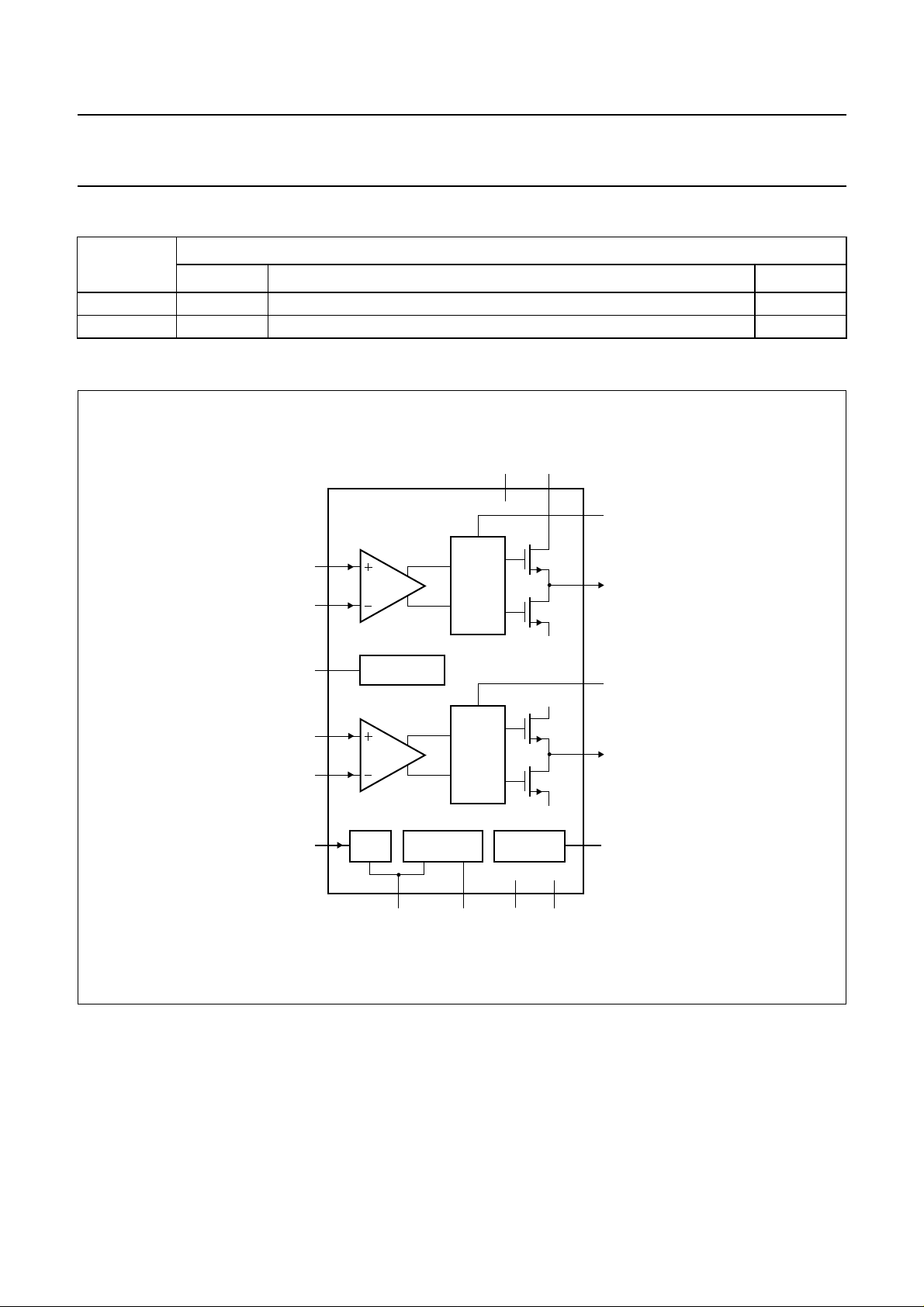
BLOCK DIAGRAM
V
handbook, full pagewidth
IN1+
IN1−
LIM
4
3
16
ANALOG
PROTECTION
V
DIGITAL
TDA8920J
DD2
13 5
V
V
DD1
SS1
DD2
6
BOOT1
7
OUT1
12
BOOT2
IN2+
IN2−
MODE
14
ANALOG
15
17
MODE OSCILLATOR STABILIZER
2
SGND
DIGITAL
1
OSC
V
SS1
Fig.1 Block diagram (SOT243-1).
11
V
SS2
9
810
V
SS2
OUT2
STAB
MGR657
1998 Dec 01 3
Page 4
Philips Semiconductors Preliminary specification
2 × 50 W class-D power amplifier TDA8920
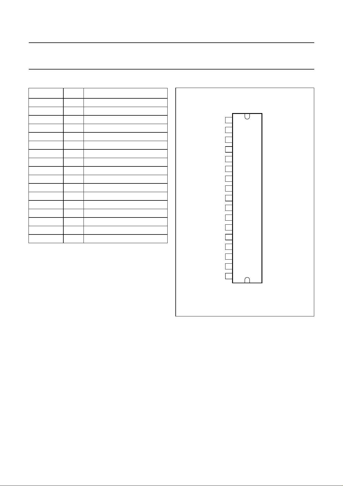
PINNING
SYMBOL PIN DESCRIPTION
OSC 1 oscillator frequency adjustment
SGND 2 signal ground (0 V)
IN1− 3 negative input channel 1
IN1+ 4 positive input channel 1
V
DD1
5 positive supply voltage 1
BOOT1 6 bootstrapping capacitor 1
OUT1 7 output 1
V
SS1
8 negative supply voltage 1; note 1
STAB 9 internal stabilizer decoupling
V
SS2
10 negative supply voltage 2; note 1
OUT2 11 output 2
BOOT2 12 bootstrapping capacitor 2
V
DD2
13 positive supply voltage 2
IN2+ 14 positive input channel 2
IN2− 15 negative input channel 2
LIM 16 current limiting adjustment
MODE 17 mode select input
Note
1. The case of the package is connected to pins 8 and 10
(V
SS1
and V
). Therefore no other voltage than V
SS2
should be connected to the case or the heatsink.
SS
handbook, halfpage
OSC
SGND
IN1−
IN1+
V
DD1
BOOT1
OUT1
V
SS1
STAB
V
SS2
OUT2
BOOT2
V
DD2
IN2+
IN2−
LIM
MODE
1
2
3
4
5
6
7
8
9
10
11
12
13
14
15
16
17
TDA8920J
MGR658
1998 Dec 01 4
Fig.2 Pin configuration (SOT243-1).
Page 5
Philips Semiconductors Preliminary specification
2 × 50 W class-D power amplifier TDA8920
FUNCTIONAL DESCRIPTION
The TDA8920 is a multi purpose audio power amplifier in
class-D technology. It contains two independent amplifiers
with high output power, high efficiency (90%), low
distortion and a low quiescent current. The amplifiers can
be connected in the following configurations:
• Mono bridge-tied load amplifier
• Stereo single-ended amplifiers.
The amplifier can be switched in three operating modes
with the mode select input:
• Standby mode, with a very low supply current
(practically zero)
• Mute mode; the amplifiers are operational but the audio
signal at the output is suppressed
• Operating mode (amplifier fully operational) with output
signal.
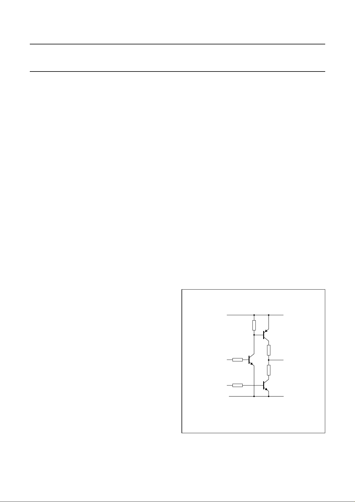
For suppressing plop noise the amplifier will remain
automatically for approximately 500 ms in the mute
mode before switching to operating mode. During this
time the coupling capacitors at the input are fully
charged. An example of a switching circuit for driving the
mode select input is illustrated in Fig.3.
Pulse Width Modulation (PWM) frequency
The output signal of the amplifier is a PWM signal with a
sample frequency of 500 kHz. The use of a second order
LC filter in the application results in an analog audio signal
across the loudspeaker. This switching frequency is fixed
by an external resistor R
connected between pin OSC
OSC
and pin SGND. With the resistor value given in the
application diagram, the oscillating frequency is typical
500 kHz. The oscillator frequency can be calculated using:
Current limiting
With an external resistor R
connected between pin LIM
LIM
and VSS the maximum output current of the amplifiers can
be set. If pin LIM is short-circuited to VSS, then the
maximum output current is limited to 7 A. The relationship
between maximum output current and resistor value is
given by:
3
I
O(max)
70.10
------------------------------------------ -
10.103R
+
A[]=
LIM
Protections
Protections are included to avoid the device being
damaged at:
• Over-temperature T
> 150 °C
j
• Short-circuit of the loudspeaker terminals: when
short-circuited the power dissipation is limited
• A maximum current limiter which limits the maximum
output current to 7 A, or to the value set by R
. During
LIM
limiting the current is measured and when the current is
higher than 7 A, the amplifier is switched off within 3 µs
and every 20 ms the IC tries to restart. The dissipation
will be low because of this low duty cycle.
• ESD protection (human body model: 3000 V and
machine model: 300 V).
handbook, halfpage
+5 V
9
5.10
f
osc
-------------R
OSC
Hz[]=
If two or more devices are used in the same audio system
it is advised to have both devices working on the same
oscillation frequency. This can be realized by connecting
all OSC pins together.
1998 Dec 01 5
R
standby/on
mute
R
MGR660
pin MODE
SGND
Fig.3 Mode select input drive circuit.
Page 6

Philips Semiconductors Preliminary specification
2 × 50 W class-D power amplifier TDA8920
LIMITING VALUES
In accordance with the Absolute Maximum Rating System (IEC 134).
SYMBOL PARAMETER CONDITIONS MIN. MAX. UNIT
V
DD
V
ms
V
sc
I
OSM
I
ORM
P
tot
T
stg
T
amb
T
vj
THERMAL CHARACTERISTICS
supply voltage −±30 V
mode select switch voltage with respect to SGND − 5.5 V
short-circuit voltage of output pins −±30 V
non-repetitive peak output current − 10 A
repetitive peak output current − 7.5 A
total power dissipation − 60 W
storage temperature −55 +150 °C
operating ambient temperature −40 +85 °C
virtual junction temperature − 150 °C
SYMBOL PARAMETER CONDITIONS VALUE UNIT
R
R
th(j-a)
th(j-c)
thermal resistance from junction to ambient in free air 40 K/W
thermal resistance from junction to case 10 K/W
QUALITY SPECIFICATION
Quality according to
“SNW-FQ-611-part E”
, if this type is used as an audio amplifier.
SWITCHING CHARACTERISTICS
V
DD
= ±25 V; T
=25°C; measured in Fig.5; unless otherwise specified.
amb
SYMBOL PARAMETER MIN. TYP. MAX. UNIT
f
osc
V
OSC(p-p)
oscillator frequency 400 500 600 kHz
voltage at tracking point (peak-to-peak value) − 1.75 − V
1998 Dec 01 6
Page 7

Philips Semiconductors Preliminary specification
2 × 50 W class-D power amplifier TDA8920
DC CHARACTERISTICS
V
= ±25 V; T
DD
SYMBOL PARAMETER CONDITIONS MIN. TYP. MAX. UNIT
Supplies
V
DD
I
q(tot)
I
stb
Amplifier outputs
V
output offset voltage on and mute −−50 mV
OO
delta output offset voltage on ↔ mute −−30 mV
∆V
OO
Mode select input; see Fig.4
V
ms
I
ms
V
th1+
V
th1−
V
ms(hys1)
V
th2+
V
th2−
V
ms(hys2)
=25°C; measured in Fig.5; unless otherwise specified.
amb
supply voltage range note 1 ±15 ±25 ±30 V
total quiescent current − 50 60 mA
standby current − 0.2 50 µA
input voltage range note 2 0 − 5.5 V
input current Vms= 5.5 V −−tbf µA
threshold voltage standby → mute; note 2 −−2V
threshold voltage mute → standby; note 2 1 −−V
hysteresis (V
th1+
) − (V
)−200 − mV
th1−
threshold voltage mute → on; note 2 −−4V
threshold voltage on → mute; note 2 3 −−V
hysteresis (V
th2+
) − (V
)−200 − mV
th2−
Notes
1. The circuit is DC adjusted at V
2. Referenced to SGND (0 V).
handbook, full pagewidth
mute
standby
= ±15Vto±30 V.
DD
on
V
th1−
V
ms(hys1)
V
th1+
V
V
th2−
ms(hys2)
Fig.4 Mode select transfer characteristic.
V
th2+
V
ms
MGR662
1998 Dec 01 7
Page 8

Philips Semiconductors Preliminary specification
2 × 50 W class-D power amplifier TDA8920
AC CHARACTERISTICS
Stereo single-ended application
= ±25 V; RL=8Ω; fi= 1 kHz; T
V
DD
SYMBOL PARAMETER CONDITIONS MIN. TYP. MAX. UNIT
P
o
output power THD = 0.5% tbf 30 − W
THD total harmonic distortion P
G
v(cl)
closed loop voltage gain 29 30 31 dB
η efficiency P
SVRR supply voltage ripple
rejection
Z
input impedance 80 120 kΩ
i
V
n(o)
α
cs
∆G
channel unbalance −−1dB
v
V
o
noise output voltage on; note 5 − 100 200 µV
channel separation note 8 50 tbf − dB
output signal mute; note 9 −−500 µV
CMRR common mode rejection ratio V
=25°C; measured in Fig.5; unless otherwise specified.
amb
THD = 10% tbf 35 − W
THD = 0.5%; Vp= ±30 V − 40 − W
THD = 10%; V
= 1 W; note 1
o
= 1 kHz − 0.1 0.15 %
f
i
f
= 10 kHz − 0.2 − %
i
= tbf W; fi= 1 kHz; note 2 85 90 − %
o
= ±30 V − 50 − W
p
on; note 3 − 60 − dB
on; note 4 tbf tbf − dB
mute; note 3 − 60 − dB
standby; note 3 − 80 − dB
on; note 6 − tbf −µV
mute; note 7 − 100 −µV
i(CM)(rms)
=1V − 65 − dB
Notes
1. Total harmonic distortion is measured in a bandwidth of 22 Hz to 22 kHz, using an 11th-order low-pass filter. When
distortion is measured using a lower order low-pass filter a significantly higher value will be found, due to the
switching frequency outside the audio band.
2. Output power measured across the loudspeaker load.
3. V
ripple=Vripple(max)
4. V
ripple=Vripple(max)
= 2 V (p-p); fi= 100 Hz; Rs=0Ω.
= 2 V (p-p); fi= 1 kHz; Rs=0Ω.
5. B = 22 Hz to 22 kHz; Rs=0Ω.
6. B = 22 Hz to 22 kHz; Rs=10kΩ.
7. B = 22 Hz to 22 kHz; independent of Rs.
8. Po= tbf W; Rs=0Ω.
9. Vi=V
= 1 V (RMS).
i(max)
1998 Dec 01 8
Page 9

Philips Semiconductors Preliminary specification
2 × 50 W class-D power amplifier TDA8920
Mono bridge-tied load application
V
= ±25 V; RL=8Ω; fi= 1 kHz; T
DD
SYMBOL PARAMETER CONDITIONS MIN. TYP. MAX. UNIT
P
o
output power THD = 0.5% tbf 100 − W
THD total harmonic distortion P
G
v(cl)
closed loop voltage gain 35 36 37 dB
η efficiency P
SVRR supply voltage ripple rejection on; note 3 − 66 − dB
Z
input impedance 40 60 − kΩ
i
V
n(o)
V
o
noise output voltage on; note 5 − 140 280 µV
output signal mute; note 8 −−tbf mV
CMRR common mode rejection ratio V
=25°C; measured in Fig.6; unless otherwise specified.
amb
THD = 10% tbf 130 − W
THD = 0.5%; V
THD = 10%; V
= 1 W; note 1
o
f
= 1 kHz − 0.1 0.15 %
i
= 10 kHz − 0.2 − %
f
i
= tbf W; fi= 1 kHz; note 2 tbf tbf − %
o
= ±30 V − 150 − W
p
= ±30 V − 190 − W
p
on; note 4 tbf −−dB
mute; note 3 − 66 − dB
standby; note 3 80 −−dB
on; note 6 − tbf −µV
mute; note 7 − 140 −µV
i(CM)(rms)
=1V − 65 − dB
Notes
1. Total harmonic distortion is measured in a bandwidth of 22 Hz to 22 kHz, using an 11th-order low-pass filter. When
distortion is measured using a lower order low-pass filter a significantly higher value will be found, due to the
switching frequency outside the audio band.
2. Output power measured across the loudspeaker load.
3. V
ripple=Vripple(max)
4. V
ripple=Vripple(max)
= 2 V (p-p); fi= 100 Hz; Rs=0Ω.
= 2 V (p-p); fi= 1 kHz; Rs=0Ω.
5. B = 22 Hz to 22 kHz; Rs=0Ω.
6. B = 22 Hz to 22 kHz; Rs=10kΩ.
7. B = 22 Hz to 22 kHz; independent of Rs.
8. Vi=V
= 1 V (RMS).
i(max)
1998 Dec 01 9
Page 10

Philips Semiconductors Preliminary specification
2 × 50 W class-D power amplifier TDA8920
APPLICATION AND TEST INFORMATION
handbook, full pagewidth
V
i1
SGND
V
i2
100 nF
100 nF
100 nF
V
DD
V
DD2VDD1
13 5
IN1+
4
IN1−
LIM
R
LIM
IN2+
IN2−
MODE
V
ms
ANALOG
3
16
PROTECTION
14
ANALOG
15
17
MODE OSCILLATOR STABILIZER
2
SGND
DIGITAL
TDA8920J
DIGITAL
1
OSC
R
OSC
10 kΩ
V
V
V
810
V
SS1
SS1
DD2
SS2
6
7
12
11
9
V
SS2
BOOT1
OUT1
BOOT2
OUT2
STAB
V
SS
SGND
C
BOOT1
47 nF
100 µH
C
BOOT2
47 nF
100 µH
C
STAB
100
nF
390
nF
390
nF
100
nF
2200
µF
8 Ω
8 Ω
2200
µF
0 V
25 V
SGND
25 V
MGR663
Maximum value of C
Filter coil is type tbf, Rs< tbfΩ.
The case of the package is internally connected to VSS.
BOOT
= tbfnF.
Fig.5 Application circuit for stereo single-ended application (SOT243-1).
1998 Dec 01 10
Page 11

Philips Semiconductors Preliminary specification
2 × 50 W class-D power amplifier TDA8920
handbook, full pagewidth
V
i
100 nF
100 nF
V
DD
V
DD2VDD1
13 5
IN1+
4
IN1−
LIM
R
LIM
IN2+
IN2−
MODE
V
ms
ANALOG
3
16
PROTECTION
14
ANALOG
15
17
MODE OSCILLATOR STABILIZER
2
SGND
DIGITAL
TDA8920J
DIGITAL
1
OSC
R
OSC
10 kΩ
V
V
V
810
V
SS1
SS1
DD2
SS2
6
7
12
11
9
V
SS2
BOOT1
OUT1
BOOT2
OUT2
STAB
V
SS
SGND
C
BOOT1
47 nF
100 µH
C
BOOT2
47 nF
100 µH
C
STAB
100
nF
390
nF
390
nF
100
nF
2200
µF
8 Ω
2200
µF
0 V
25 V
SGND
25 V
MGR664
Maximum value of C
Filter coil is type tbf, Rs< tbfΩ.
The case of the package is internally connected to VSS.
BOOT
= tbfnF.
Fig.6 Application circuit for mono bridge-tied load application (SOT243-1).
1998 Dec 01 11
Page 12

Philips Semiconductors Preliminary specification
2 × 50 W class-D power amplifier TDA8920
PACKAGE OUTLINES
DBS17P: plastic DIL-bent-SIL power package; 17 leads (lead length 12 mm)
non-concave
D
d
j
x
E
h
view B: mounting base side
B
SOT243-1
D
h
A
2
E
A
117
e
0.48
0.38
1
e
(1)
deD
24.0
20.0
23.6
19.6
Z
DIMENSIONS (mm are the original dimensions)
UNIT A e
mm
Note
1. Plastic or metal protrusions of 0.25 mm maximum per side are not included.
OUTLINE
VERSION
SOT243-1
A2bpcD
17.0
4.6
4.2
0.75
0.60
15.5
IEC JEDEC EIAJ
w M
b
p
(1)
E
h
12.2
10 2.54
11.8
REFERENCES
0 5 10 mm
scale
1
1.27
e
5.08
L
3
L
E
2
h
6
Q
LL3m
3.4
12.4
3.1
11.0
m
2.4
1.6
c
e
2
Qj
2.1
4.3
1.8
EUROPEAN
PROJECTION
v M
v
0.8
x
0.4w0.03
ISSUE DATE
95-03-11
97-12-16
(1)
Z
2.00
1.45
1998 Dec 01 12
Page 13

Philips Semiconductors Preliminary specification
2 × 50 W class-D power amplifier TDA8920
HSOP20: heatsink small outline package; 20 leads
D
y
D
1
1
pin 1 index
10
SOT418-1
E
x
c
E
2
H
E
D
2
A
E
1
2
A
1
A
X
v M
A
Q
A
(A3)
20
Z
DIMENSIONS (mm are the original dimensions)
A
UNIT
mm
Note
1. Plastic or metal protrusions of 0.25 mm maximum per side are not included.
A
1
max.
0.3
3.7 0.35
0.1
OUTLINE
VERSION
SOT418-1
e
A
3.5
3.2
2
bpc
A
3
0.53
0.40
IEC JEDEC EIAJ
0.32
0.23
D
16.0
15.8
(1)
D
13.0
12.6
11
w M
b
p
0 5 10 mm
scale
(1)
D
2
1
1.1
0.9
REFERENCES
E
11.1
10.9
E
6.2
5.8
1
E
2.9
2.5
L
detail X
H
L
Q
e
E
14.5
13.9
p
1.1
0.8
2
1.27
v
1.7
0.25w0.25
1.5
EUROPEAN
PROJECTION
p
x
0.03
θ
yZ
2.5
0.1
2.0
ISSUE DATE
97-11-03
98-02-25
θ
8°
0°
1998 Dec 01 13
Page 14

Philips Semiconductors Preliminary specification
2 × 50 W class-D power amplifier TDA8920
SOLDERING
Introduction
This text gives a very brief insight to a complex technology.
A more in-depth account of soldering ICs can be found in
our
“Data Handbook IC26; Integrated Circuit Packages”
(document order number 9398 652 90011).
There is no soldering method that is ideal for all IC
packages. Wave soldering is often preferred when
through-hole and surface mount components are mixed on
one printed-circuit board. However, wave soldering is not
always suitable for surface mount ICs, or for printed-circuit
boards with high population densities. In these situations
reflow soldering is often used.
Through-hole mount packages
S
OLDERING BY DIPPING OR BY SOLDER WAVE
The maximum permissible temperature of the solder is
260 °C; solder at this temperature must not be in contact
with the joints for more than 5 seconds. The total contact
time of successive solder waves must not exceed
5 seconds.
The device may be mounted up to the seating plane, but
the temperature of the plastic body must not exceed the
specified maximum storage temperature (T
stg(max)
). If the
printed-circuit board has been pre-heated, forced cooling
may be necessary immediately after soldering to keep the
temperature within the permissible limit.
M
ANUAL SOLDERING
Apply the soldering iron (24 V or less) to the lead(s) of the
package, either below the seating plane or not more than
2 mm above it. If the temperature of the soldering iron bit
is less than 300 °C it may remain in contact for up to
10 seconds. If the bit temperature is between
300 and 400 °C, contact may be up to 5 seconds.
Surface mount packages
REFLOW SOLDERING
Reflow soldering requires solder paste (a suspension of
fine solder particles, flux and binding agent) to be applied
to the printed-circuit board by screen printing, stencilling or
pressure-syringe dispensing before package placement.
Several methods exist for reflowing; for example,
infrared/convection heating in a conveyor type oven.
Throughput times (preheating, soldering and cooling) vary
between 100 and 200 seconds depending on heating
method.
Typical reflow peak temperatures range from
215 to 250 °C. The top-surface temperature of the
packages should preferable be kept below 230 °C.
W
AVE SOLDERING
Conventional single wave soldering is not recommended
for surface mount devices (SMDs) or printed-circuit boards
with a high component density, as solder bridging and
non-wetting can present major problems.
To overcome these problems the double-wave soldering
method was specifically developed.
If wave soldering is used the following conditions must be
observed for optimal results:
• Use a double-wave soldering method comprising a
turbulent wave with high upward pressure followed by a
smooth laminar wave.
• For packages with leads on two sides and a pitch (e):
– larger than or equal to 1.27 mm, the footprint
longitudinal axis is preferred to be parallel to the
transport direction of the printed-circuit board;
– smaller than 1.27 mm, the footprint longitudinal axis
must be parallel to the transport direction of the
printed-circuit board.
The footprint must incorporate solder thieves at the
downstream end.
• For packages with leads on four sides, the footprint must
be placed at a 45° angle to the transport direction of the
printed-circuit board. The footprint must incorporate
solder thieves downstream and at the side corners.
During placement and before soldering, the package must
be fixed with a droplet of adhesive. The adhesive can be
applied by screen printing, pin transfer or syringe
dispensing. The package can be soldered after the
adhesive is cured.
Typical dwell time is 4 seconds at 250 °C.
A mildly-activated flux will eliminate the need for removal
of corrosive residues in most applications.
ANUAL SOLDERING
M
Fix the component by first soldering two
diagonally-opposite end leads. Use a low voltage (24 V or
less) soldering iron applied to the flat part of the lead.
Contact time must be limited to 10 seconds at up to
300 °C.
When using a dedicated tool, all other leads can be
soldered in one operation within 2 to 5 seconds between
270 and 320 °C.
1998 Dec 01 14
Page 15

Philips Semiconductors Preliminary specification
2 × 50 W class-D power amplifier TDA8920
Suitability of IC packages for wave, reflow and dipping soldering methods
MOUNTING PACKAGE
Through-hole mount DBS, DIP, HDIP, SDIP, SIL suitable
WAVE REFLOW
(2)
− suitable
(1)
DIPPING
Surface mount BGA, SQFP not suitable suitable −
SOLDERING METHOD
HLQFP, HSQFP, HSOP, HTSSOP, SMS not suitable
(4)
PLCC
, SO, SOJ suitable suitable −
LQFP, QFP, TQFP not recommended
SSOP, TSSOP, VSO not recommended
(3)
(4)(5)
(6)
suitable −
suitable −
suitable −
Notes
1. All surface mount (SMD) packages are moisture sensitive. Depending upon the moisture content, the maximum
temperature (with respect to time) and body size of the package, there is a risk that internal or external package
cracks may occur due to vaporization of the moisture in them (the so called popcorn effect). For details, refer to the
Drypack information in the
“Data Handbook IC26; Integrated Circuit Packages; Section: Packing Methods”
.
2. For SDIP packages, the longitudinal axis must be parallel to the transport direction of the printed-circuit board.
3. These packages are not suitable for wave soldering as a solder joint between the printed-circuit board and heatsink
(at bottom version) can not be achieved, and as solder may stick to the heatsink (on top version).
4. If wave soldering is considered, then the package must be placed at a 45° angle to the solder wave direction.
The package footprint must incorporate solder thieves downstream and at the side corners.
5. Wave soldering is only suitable for LQFP, QFP and TQFP packages with a pitch (e) equal to or larger than 0.8 mm;
it is definitely not suitable for packages with a pitch (e) equal to or smaller than 0.65 mm.
6. Wave soldering is only suitable for SSOP and TSSOP packages with a pitch (e) equal to or larger than 0.65 mm; it is
definitely not suitable for packages with a pitch (e) equal to or smaller than 0.5 mm.
DEFINITIONS
Data sheet status
Objective specification This data sheet contains target or goal specifications for product development.
Preliminary specification This data sheet contains preliminary data; supplementary data may be published later.
Product specification This data sheet contains final product specifications.
Limiting values
Limiting values given are in accordance with the Absolute Maximum Rating System (IEC 134). Stress above one or
more of the limiting values may cause permanent damage to the device. These are stress ratings only and operation
of the device at these or at any other conditions above those given in the Characteristics sections of the specification
is not implied. Exposure to limiting values for extended periods may affect device reliability.
Application information
Where application information is given, it is advisory and does not form part of the specification.
LIFE SUPPORT APPLICATIONS
These products are not designed for use in life support appliances, devices, or systems where malfunction of these
products can reasonably be expected to result in personal injury. Philips customers using or selling these products for
use in such applications do so at their own risk and agree to fully indemnify Philips for any damages resulting from such
improper use or sale.
1998 Dec 01 15
Page 16

Philips Semiconductors – a worldwide company
Argentina: see South America
Australia: 34 Waterloo Road, NORTH RYDE, NSW 2113,
Tel. +61 2 9805 4455, Fax. +61 2 9805 4466
Austria: Computerstr. 6, A-1101 WIEN, P.O. Box 213, Tel. +43 160 1010,
Fax. +43 160 101 1210
Belarus: Hotel Minsk Business Center, Bld. 3, r. 1211, Volodarski Str. 6,
220050 MINSK, Tel. +375 172 200 733, Fax. +375 172 200 773
Belgium: see The Netherlands
Brazil: see South America
Bulgaria: Philips Bulgaria Ltd., Energoproject, 15th floor,
51 James Bourchier Blvd., 1407 SOFIA,
Tel. +359 2 689 211, Fax. +359 2 689 102
Canada: PHILIPS SEMICONDUCTORS/COMPONENTS,
Tel. +1 800 234 7381
China/Hong Kong: 501 Hong Kong Industrial Technology Centre,
72 Tat Chee Avenue, Kowloon Tong, HONG KONG,
Tel. +852 2319 7888, Fax. +852 2319 7700
Colombia: see South America
Czech Republic: see Austria
Denmark: Prags Boulevard 80, PB 1919, DK-2300 COPENHAGEN S,
Tel. +45 32 88 2636, Fax. +45 31 57 0044
Finland: Sinikalliontie 3, FIN-02630 ESPOO,
Tel. +358 9 615800, Fax. +358 9 61580920
France: 51 Rue Carnot, BP317, 92156 SURESNES Cedex,
Tel. +33 1 40 99 6161, Fax. +33 1 40 99 6427
Germany: Hammerbrookstraße 69, D-20097 HAMBURG,
Tel. +49 40 23 53 60, Fax. +49 40 23 536 300
Greece: No. 15, 25th March Street, GR 17778 TAVROS/ATHENS,
Tel. +30 1 4894 339/239, Fax. +30 1 4814 240
Hungary: see Austria
India: Philips INDIA Ltd, Band Box Building, 2nd floor,
254-D, Dr. Annie Besant Road, Worli, MUMBAI 400 025,
Tel. +91 22 493 8541, Fax. +91 22 493 0966
Indonesia: PT Philips Development Corporation, Semiconductors Division,
Gedung Philips, Jl. Buncit Raya Kav.99-100, JAKARTA 12510,
Tel. +62 21 794 0040 ext. 2501, Fax. +62 21 794 0080
Ireland: Newstead, Clonskeagh, DUBLIN 14,
Tel. +353 1 7640 000, Fax. +353 1 7640 200
Israel: RAPAC Electronics, 7 Kehilat Saloniki St, PO Box 18053,
TEL AVIV 61180, Tel. +972 3 645 0444, Fax. +972 3 649 1007
Italy: PHILIPS SEMICONDUCTORS, Piazza IV Novembre 3,
20124 MILANO, Tel. +39 2 6752 2531, Fax. +39 2 6752 2557
Japan: Philips Bldg 13-37, Kohnan 2-chome, Minato-ku,
TOKYO 108-8507, Tel. +81 3 3740 5130, Fax. +81 3 3740 5077
Korea: Philips House, 260-199 Itaewon-dong, Yongsan-ku, SEOUL,
Tel. +82 2 709 1412, Fax. +82 2 709 1415
Malaysia: No. 76 Jalan Universiti, 46200 PETALING JAYA, SELANGOR,
Tel. +60 3 750 5214, Fax. +60 3 757 4880
Mexico: 5900 Gateway East, Suite 200, EL PASO, TEXAS 79905,
Tel. +9-5 800 234 7381
Middle East: see Italy
Netherlands: Postbus 90050, 5600PB EINDHOVEN, Bldg. VB,
Tel. +31 40 27 82785, Fax. +31 40 27 88399
New Zealand: 2 Wagener Place, C.P.O. Box 1041, AUCKLAND,
Tel. +64 9 849 4160, Fax. +64 9 849 7811
Norway: Box 1, Manglerud 0612, OSLO,
Tel. +47 22 74 8000, Fax. +47 22 74 8341
Pakistan: see Singapore
Philippines: Philips Semiconductors Philippines Inc.,
106 Valero St. Salcedo Village, P.O. Box 2108 MCC, MAKATI,
Metro MANILA, Tel. +63 2 816 6380, Fax. +63 2 817 3474
Poland: Ul. Lukiska 10, PL 04-123 WARSZAWA,
Tel. +48 22 612 2831, Fax. +48 22 612 2327
Portugal: see Spain
Romania: see Italy
Russia: Philips Russia, Ul. Usatcheva 35A, 119048 MOSCOW,
Tel. +7 095 755 6918, Fax. +7 095 755 6919
Singapore: Lorong 1, Toa Payoh, SINGAPORE 319762,
Tel. +65 350 2538, Fax. +65 251 6500
Slovakia: see Austria
Slovenia: see Italy
South Africa: S.A. PHILIPS Pty Ltd., 195-215 Main Road Martindale,
2092 JOHANNESBURG, P.O. Box 7430 Johannesburg 2000,
Tel. +27 11 470 5911, Fax. +27 11 470 5494
South America: Al. Vicente Pinzon, 173, 6th floor,
04547-130 SÃO PAULO, SP, Brazil,
Tel. +55 11 821 2333, Fax. +55 11 821 2382
Spain: Balmes 22, 08007 BARCELONA,
Tel. +34 93 301 6312, Fax. +34 93 301 4107
Sweden: Kottbygatan 7, Akalla, S-16485 STOCKHOLM,
Tel. +46 8 5985 2000, Fax. +46 8 5985 2745
Switzerland: Allmendstrasse 140, CH-8027 ZÜRICH,
Tel. +41 1 488 2741 Fax. +41 1 488 3263
Taiwan: Philips Semiconductors, 6F, No. 96, Chien Kuo N. Rd., Sec. 1,
TAIPEI, Taiwan Tel. +886 2 2134 2865, Fax. +886 2 2134 2874
Thailand: PHILIPS ELECTRONICS (THAILAND) Ltd.,
209/2 Sanpavuth-Bangna Road Prakanong, BANGKOK 10260,
Tel. +66 2 745 4090, Fax. +66 2 398 0793
Turkey: Talatpasa Cad. No. 5, 80640 GÜLTEPE/ISTANBUL,
Tel. +90 212 279 2770, Fax. +90 212 282 6707
Ukraine: PHILIPS UKRAINE, 4 Patrice Lumumba str., Building B, Floor 7,
252042 KIEV, Tel. +380 44 264 2776, Fax. +380 44 268 0461
United Kingdom: Philips Semiconductors Ltd., 276 Bath Road, Hayes,
MIDDLESEX UB3 5BX, Tel. +44 181 730 5000, Fax. +44 181 754 8421
United States: 811 East Arques Avenue, SUNNYVALE, CA 94088-3409,
Tel. +1 800 234 7381
Uruguay: see South America
Vietnam: see Singapore
Yugoslavia: PHILIPS, Trg N. Pasica 5/v, 11000 BEOGRAD,
Tel. +381 11 625 344, Fax.+381 11 635 777
For all other countries apply to: Philips Semiconductors,
International Marketing & Sales Communications, Building BE-p, P.O. Box 218,
5600 MD EINDHOVEN, The Netherlands, Fax. +31 40 27 24825
© Philips Electronics N.V. 1998 SCA60
All rights are reserved. Reproduction in whole or in part is prohibited without the prior written consent of the copyright owner.
The information presented in this document does not form part of any quotation or contract, is believed to be accurate and reliable and may be changed
without notice. No liability will be accepted by the publisher for any consequence of its use. Publication thereof does not convey nor imply any license
under patent- or other industrial or intellectual property rights.
Internet: http://www.semiconductors.philips.com
Printed in The Netherlands 545102/25/01/pp16 Date of release: 1998 Dec 01 Document order number: 9397 750 04343
 Loading...