

Page 1

INTEGRATED CIRCUITS
DATA SH EET
TDA8776
10-bit, 500 Msps Digital-to-Analog
Converter (DAC)
Product specification
Supersedes data of 1995 Mar 28
File under Integrated Circuits, IC02
1996 Jun 04
Page 2
Philips Semiconductors Product specification
10-bit, 500 Msps Digital-to-Analog
TDA8776
Converter (DAC)
FEATURES
• 10-bit resolution
• Conversion rate up to 500 MHz
• 10K/100K ECL input levels
• Internal reference voltage generator
• No deglitching circuit required
• Internal input register
• Power dissipation only 925 mW (typical)
• Internal 50 Ω output load (connected to the analog
ground)
• Very few external components required.
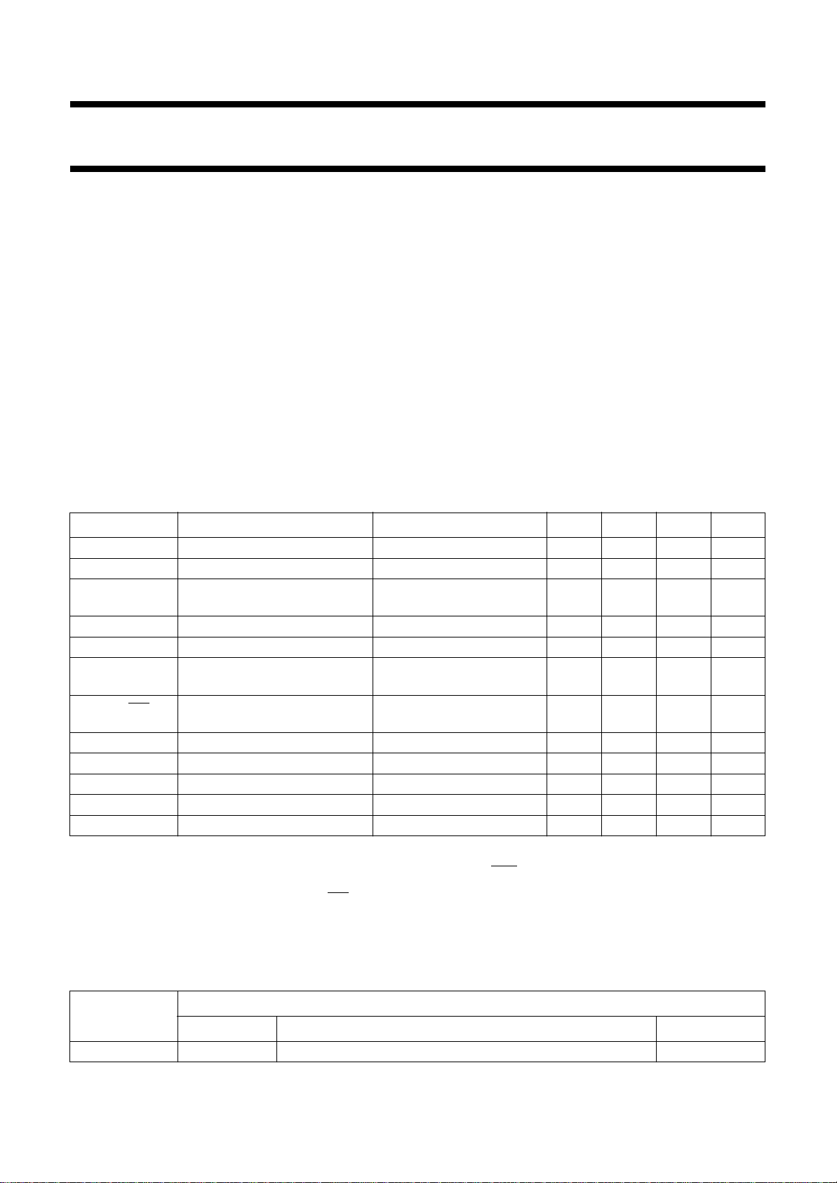
QUICK REFERENCE DATA
SYMBOL PARAMETER CONDITIONS MIN. TYP. MAX. UNIT
V
V
V
EEA
EED
EEI
analog supply voltage −5.46 −5.20 −4.94 V
digital supply voltage −5.46 −5.20 −4.94 V
input stages digital supply
note 1 −5.46 −5.20 −4.94 V
voltage
I
EEA
I
EED
I
EEI
analog supply current note 1 − 108 145 mA
digital supply current note 1 − 60 85 mA
input stages digital supply
note 1 − 10 15 mA
current
V
OUT
− V
OUT
full-scale analog output voltage
notes 1 and 2; ZL=50Ω 1.7 2.0 2.5 V
(peak-to-peak value)
INL DC integral non-linearity note 3 −±0.3 ±0.5 LSB
DNL DC differential non-linearity note 3 −±0.2 ±0.45 LSB
f
clk(max)
t
S1
P
tot
maximum clock frequency 500 −−MHz
settling time (differential) 10% to 90% full scale; Fig.9 − 0.5 − ns
total power dissipation − 925 − mW
APPLICATIONS
High-speed digital-to-analog conversion for:
• High resolution video and graphics
• Direct Digital Synthesis (DDS)
• Telecommunication
• High-speed modems.
GENERAL DESCRIPTION
The TDA8776 is a 10-bit Digital-to-Analog Converter
(DAC) for high resolution video and other high frequency
applications. It converts the digital input signal into an
analog output voltage at a maximum conversion rate of
500 Msps. No external reference voltage is required and
all digital inputs are 10K/100K-ECL compatible.
Notes
1. D0 to D9 connected to either HIGH or LOW level, CLK is HIGH and CLK is LOW.
2. The analog output voltages (V
resistance between AGND and each of these outputs is typically 50 Ω.
3. A warm-up time is necessary to reach optimal performances.
ORDERING INFORMATION
TYPE NUMBER
TDA8776K PLCC28 plastic leaded chip carrier; 28 leads SOT261-2
1996 Jun 04 2
OUT
and V
) are negative with respect to AGND (see Table 1). The external output
OUT
PACKAGE
NAME DESCRIPTION VERSION
Page 3
Philips Semiconductors Product specification
10-bit, 500 Msps Digital-to-Analog
Converter (DAC)
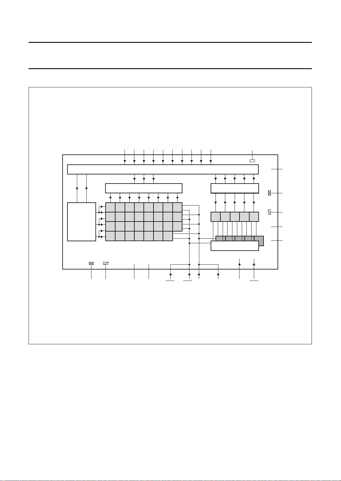
BLOCK DIAGRAM
handbook, full pagewidth
ROW
DECODER
D9 D8 D7 D6 D5 D4 D3 D2
22 21 20 19 18 17 16 15 14 13 12
COLUMN DECODER
TDA8776
ECL BUFFERS
D1 D0 IGND
DELAY
R-2R DIVIDER
TDA8776
25
V
EEI
28
DGND2
10
AGND2
11
V
EED3
24
V
EEA
25 34 9 86 7 27
DGND1
AGND1
V
EED1VEED2
V
OUT2
V
OUT1VOUT1VOUT2
Fig.1 Block diagram.
26
MLD200
CLK CLK
1996 Jun 04 3
Page 4
Philips Semiconductors Product specification
10-bit, 500 Msps Digital-to-Analog
Converter (DAC)
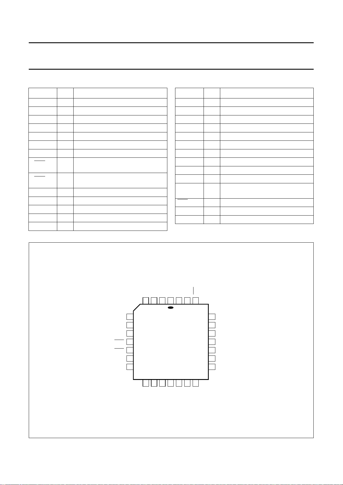
PINNING
SYMBOL PIN DESCRIPTION
n.c. 1 not connected
DGND1 2 digital ground 1
V
EED1
V
EED2
AGND1 5 analog ground 1
V
OUT1
V
OUT2
V
OUT1
V
OUT2
AGND2 10 analog ground 2
V
EED3
IGND 12 input ground for ECL input buffers
D0 13 data input; bit 0 (LSB)
D1 14 data input; bit 1
3 digital supply voltage 1 (−5.2 V)
4 digital supply voltage 2 (−5.2 V)
6 analog voltage output 1
7 analog voltage output 2
8 complementary analog voltage
output 1
9 complementary analog voltage
output 2
11 digital supply voltage 3 (−5.2 V)
TDA8776
SYMBOL PIN DESCRIPTION
D2 15 data input; bit 2
D3 16 data input; bit 3
D4 17 data input; bit 4
D5 18 data input; bit 5
D6 19 data input; bit 6
D7 20 data input; bit 7
D8 21 data input; bit 8
D9 22 data input; bit 9 (MSB)
n.c. 23 not connected
V
EEA
V
EEI
CLK 26 complementary clock input
CLK 27 clock input
DGND2 28 digital ground 2
24 analog supply voltage (−5.2 V)
25 input supply voltage for ECL input
buffers (−5.2 V)
handbook, halfpage
EED2VEED1
AGND1
V
OUT1
V
OUT2
V
OUT1
V
OUT2
AGND2
V
EED3
V
5
6
7
8
9
10
11
4
12
IGND
DGND1
3
2
TDA8776
13
14
D0
D1D2D3
Fig.2 Pin configuration.
1996 Jun 04 4
n.c.
1
15
CLK
DGND2
28
27
16
17
D4
CLK
26
18
D5
25
24
23
22
21
20
19
MLD201
V
V
n.c.
D9
D8
D7
D6
EEI
EEA
Page 5
Philips Semiconductors Product specification
10-bit, 500 Msps Digital-to-Analog
TDA8776
Converter (DAC)
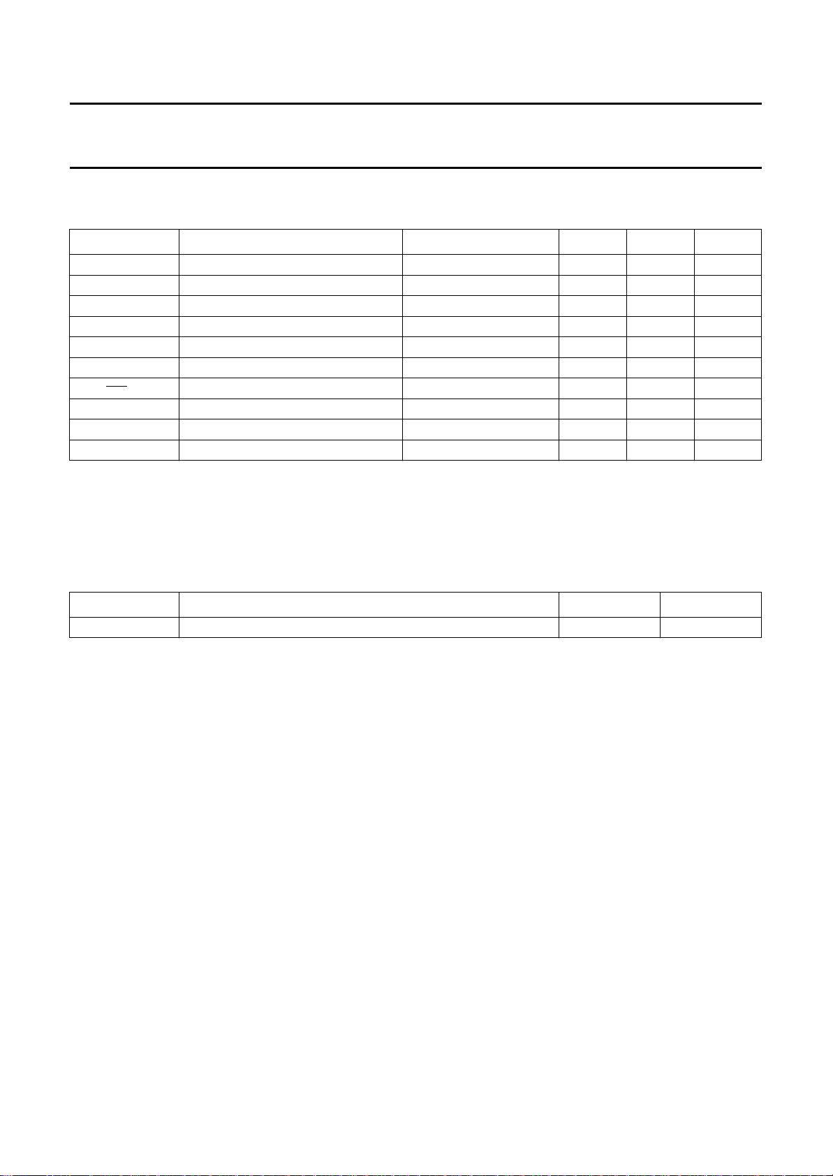
LIMITING VALUES
In accordance with the Absolute Maximum Rating System (IEC 134).
SYMBOL PARAMETER CONDITIONS MIN. MAX. UNIT
V
EEA
V
EED
V
EEI
− V
V
EEA
EED
AGND − DGND ground voltage differential −0.1 +0.1 V
V
I
I
OUT/IOUT
T
stg
T
amb
T
j
HANDLING
Inputs and outputs are protected against electrostatic discharges in normal handling. However, to be totally safe, it is
desirable to take normal precautions appropriate to handling integrated circuits.
analog supply voltage −7.0 ±0.3 V
digital supply voltage −7.0 ±0.3 V
input stages digital supply voltage −7.0 ±0.3 V
supply voltage differential −0.5 +0.5 V
input voltage V
EEI
±0.3 V
total output current ZL=50Ω−5 +50 mA
storage temperature −55 +150 °C
operating ambient temperature 0 +70 °C
junction temperature − +150 °C
THERMAL CHARACTERISTICS
SYMBOL PARAMETER VALUE UNIT
R
th j-a
thermal resistance from junction to ambient in free air 55 (typ.) K/W
1996 Jun 04 5
Page 6
Philips Semiconductors Product specification
10-bit, 500 Msps Digital-to-Analog
TDA8776
Converter (DAC)
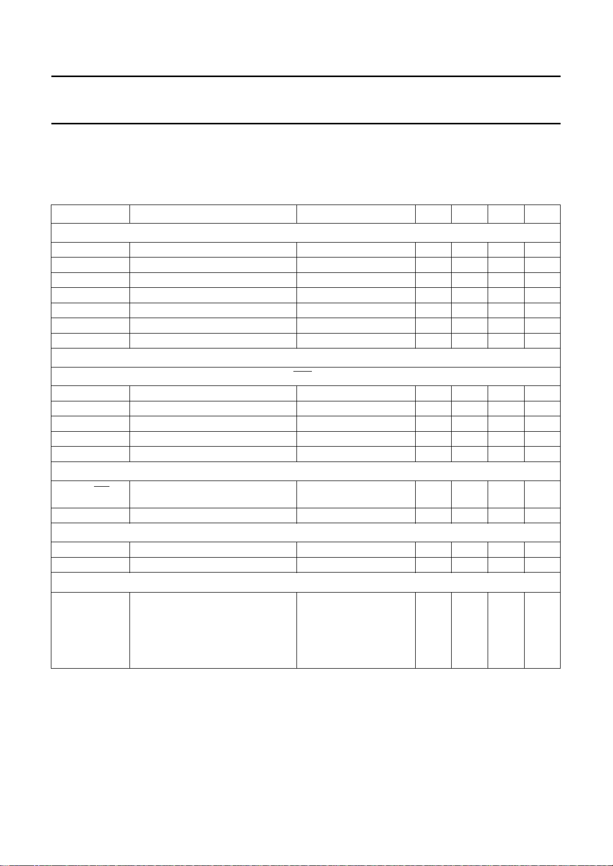
CHARACTERISTICS
V
EEA=V24
V
EEI=V25
shorted together; V
V
EEA=VEED
Supply
V
EEA
V
EED
V
EEI
I
EEA
I
EED
I
EEI
AGND − DGND ground voltage differential −0.1 − +0.1 V
Inputs
DIGITAL INPUTS (D9 TO D0) AND CLOCK INPUTS (CLK AND CLK)
V
IL
V
IH
I
IL
I
IH
f
clk(max)
Outputs (referenced to AGND); notes 1 and 2
V
OUT
Z
O
Transfer function
INL DC integral non-linearity note 3 −±0.3 ±0.5 LSB
DNL DC differential non-linearity note 3 −±0.2 ±0.45 LSB
to V5and V10= −5.46 to −4.94 V; V
to V12= −5.46 to −4.94 V; V
− V
OUT
= −5.2 V and T
= 2 V (p-p); ZL=50Ω; unless otherwise specified (typical values measured at
OUT
=25°C).
amb
EED
and V
EED=V3,V4
shorted together; T
EEI
and V11to V2and V28= −5.46 to −4.94 V;
= 0 to +70 °C; AGND, DGND and IGND
amb
SYMBOL PARAMETER CONDITIONS MIN. TYP. MAX. UNIT
analog supply voltage −5.46 −5.20 −4.94 V
digital supply voltage −5.46 −5.20 −4.94 V
input stages digital supply voltage note 1 −5.46 −5.20 −4.94 V
analog supply current note 1 − 108 145 mA
digital supply current note 1 − 60 85 mA
input stages digital supply current note 1 − 10 15 mA
LOW level input voltage −1.9 −1.8 −1.6 V
HIGH level input voltage −1.2 −0.9 −0.8 V
LOW level input current VI= −1.8 V −−10 µA
HIGH level input current VI= −0.9 V −−20 µA
maximum clock frequency 500 −−MHz
− V
OUT
full-scale analog output voltage
ZL=50Ω 1.7 2.0 2.5 V
(peak-to-peak value)
output impedance − 50 −Ω
Spurious free dynamic range (f
SFDR spurious free dynamic range
1996 Jun 04 6
= 500 MHz); V
clk
= 10 MHz −65 −69 − dB
f
OUT
= 50 MHz −−60 − dB
f
OUT
= 80 MHz −−59 − dB
f
OUT
= 100 MHz −52 −59 − dB
f
OUT
EEA=VEED
= 5.2 V; T
=25°C; note 4; see Fig.3
amb
Page 7
Philips Semiconductors Product specification
10-bit, 500 Msps Digital-to-Analog
TDA8776
Converter (DAC)
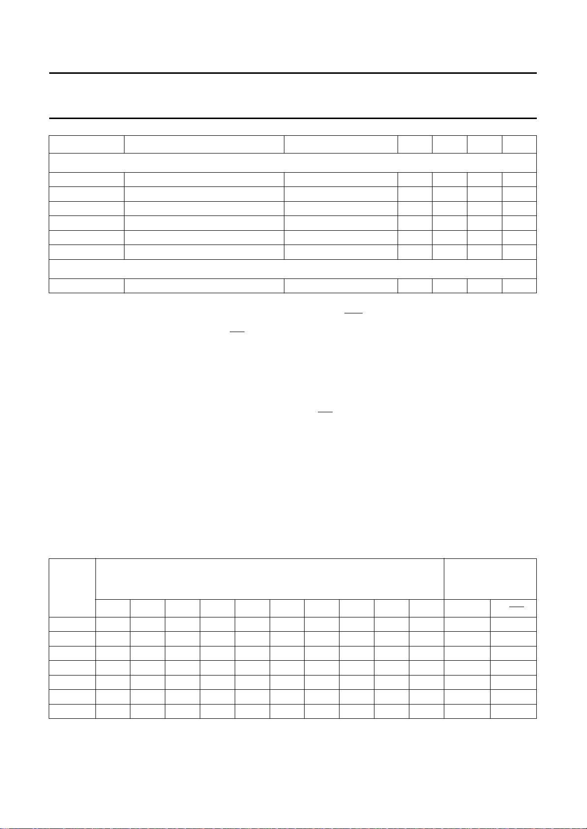
SYMBOL PARAMETER CONDITIONS MIN. TYP. MAX. UNIT
Switching characteristics (f
t
SU;DAT
t
HD;DAT
t
PD
t
S1
t
S2
t
d
data set-up time − 400 500 ps
data hold time 100 150 − ps
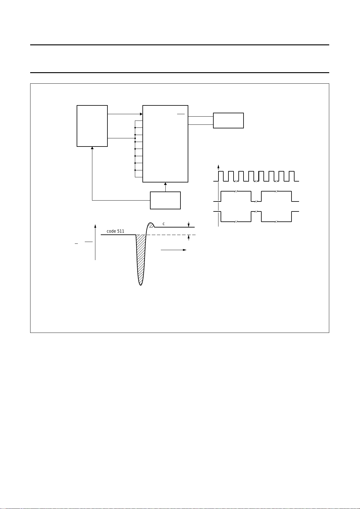
propagation delay time − 0.8 0.9 ns
settling time 10% to 90% full scale − 0.5 − ns
settling time change to ±1 LSB − 2.0 − ns
input to 50% output delay time − 1.4 1.5 ns
Output transients; glitches (f
E
g
differential glitch energy from code transition 511 to 512 − 12pV.s
Notes
1. D0 to D9 connected to either HIGH or LOW level, CLK is HIGH and CLK is LOW.
2. The analog output voltages (V
resistance between AGND and each of these outputs is typically 50 Ω.
3. Due to on-chip regulator behaviour a warm-up time is necessary to reach optimal performances; a typical time is
1 minute.
4. Devices with higher SFDR (min.) can be delivered on request.
5. The worst case characteristics are obtained at the transition from input code 0 to 1023 and if an external load
impedance greater than 50 Ω is connected between V
The specified values have been measured directly on a 50 Ω load between V
impedance between V
6. The data set-up (t
SU;DAT
stable in order to be correctly registered. A negative set-up time indicates that the data may be initiated after the
falling edge of the clock and still be recognized. The data hold time (t
falling edge of the clock that the input data must be stable in order to be correctly registered. A negative hold time
indicates that the data may be released prior to the falling edge of the clock and still be recognized.
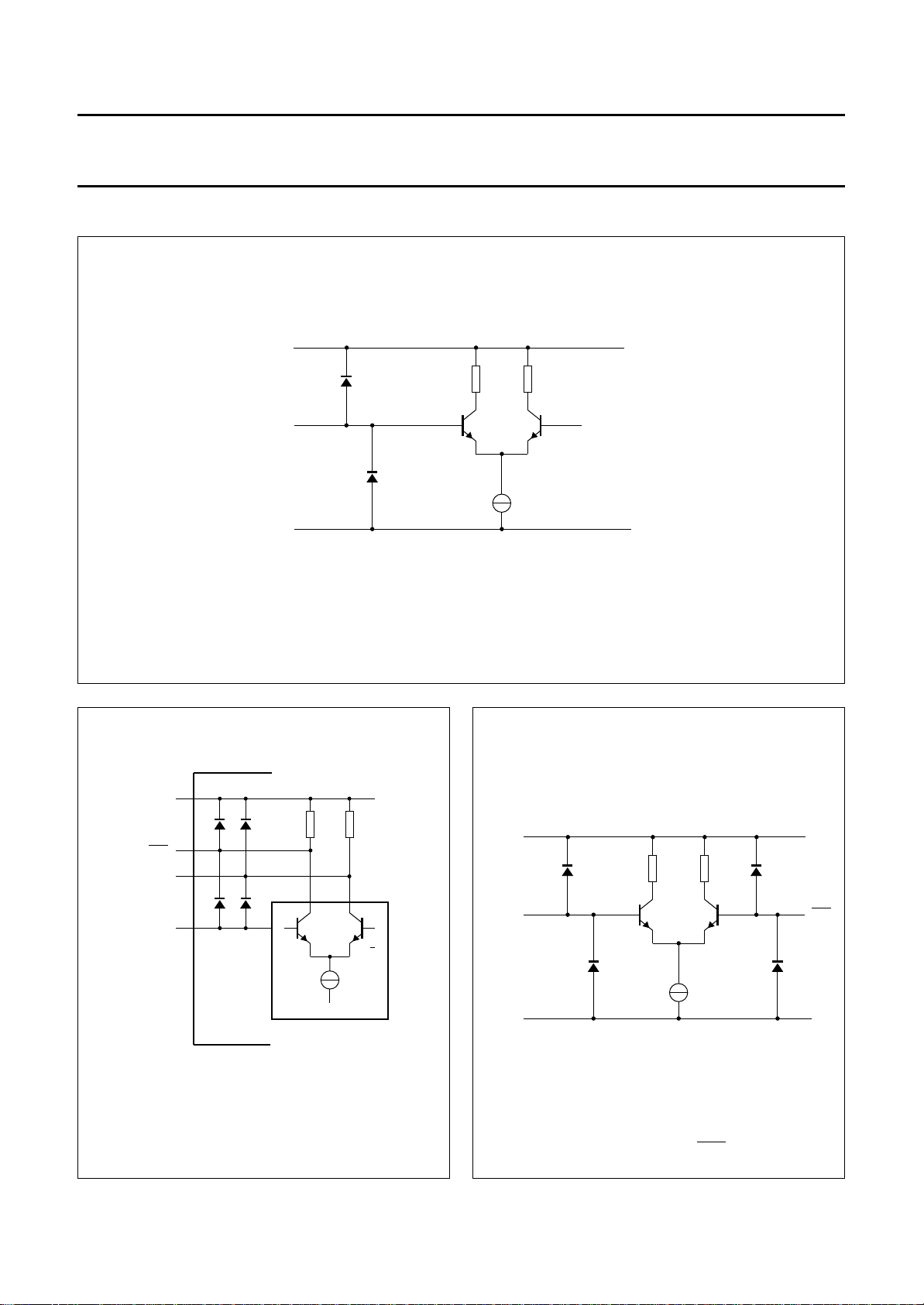
7. The definition of glitch energy and the measurement set-up are shown in Fig.10. The glitch energy is measured at
the input transition between code 511 to 512.
= 500 MHz); notes 5 and 6; see Figs 8 and 9
clk
= 500 MHz); note 7; see Fig.10
clk
and V
OUT
and AGND has been applied. All input data is latched at the falling edge of the clock.
OUT
) are negative with respect to AGND (see Table 1). The external output
OUT
OUT
or V
and AGND in parallel with the external 50 Ω load.
OUT
and AGND. No further load
OUT
) is the minimum period preceding the falling edge of the clock that the input data must be
) is the minimum period following the
HD;DAT
Table 1 Input coding and DAC output voltages (typical values; referenced to AGND regardless of the offset voltage)
CODE
D9 D8 D7 D6 D5 D4 D3 D2 D1 D0 V
0 0000000000 0 −1.0
1 0000000001−0.0010 −0.9990
. .......... . .
5121000000000−0.5 −0.5
. .......... . .
1022 1111111110−0.9990 −0.0010
1023 1111111111−1.0 0
1996 Jun 04 7
BINARY INPUT DATA
DAC OUTPUT
VOLTAGES (V)
Z
=50Ω
L
OUT
V
OUT
Page 8
Philips Semiconductors Product specification
10-bit, 500 Msps Digital-to-Analog
Converter (DAC)
75
handbook, full pagewidth
SFDR
(dB)
70
65
60
55
TDA8776
MGD479
50
1
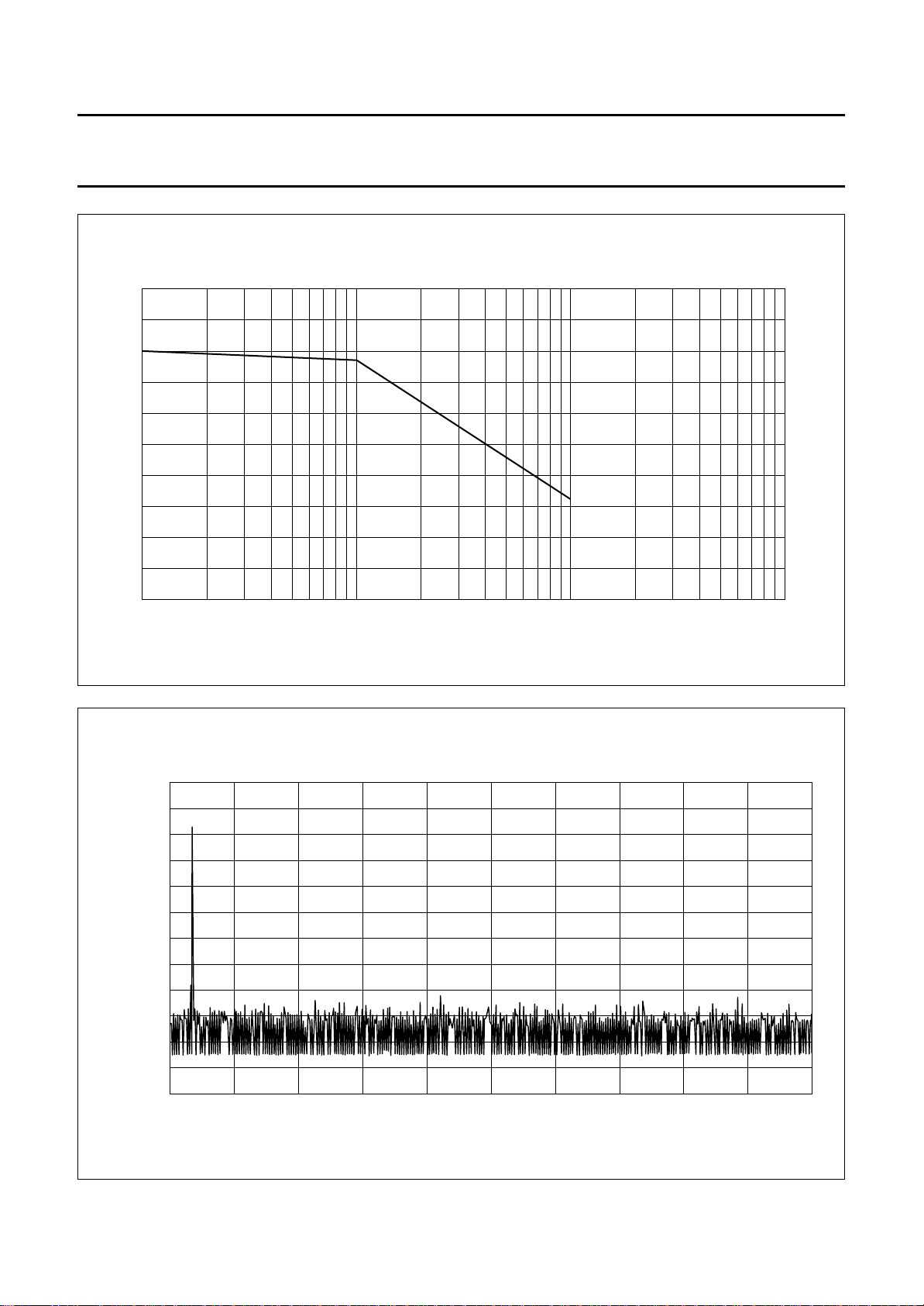
Fig.3 Typical spurious free dynamic range (SFDR) as a function of output frequency.
20
handbook, full pagewidth
DAC
OUTPUT
SPECTRUM
(dB)
0
−20
−40
−60
−80
2
10
10
f (MHz)
3
10
MGD470
−100
0 50 100 150 200
1996 Jun 04 8
Fig.4 Typical output spectrum; f
= 500 MHz; f
clk
= 10 MHz.
OUT
f (MHz)
250
Page 9
Philips Semiconductors Product specification
10-bit, 500 Msps Digital-to-Analog
Converter (DAC)
20
handbook, full pagewidth
DAC
OUTPUT
SPECTRUM
(dB)
0
−20
−40
−60
−80
TDA8776
MGD471
−100
0 50 100 150 200
20
handbook, full pagewidth
DAC
OUTPUT
SPECTRUM
(dB)
0
−20
−40
−60
−80
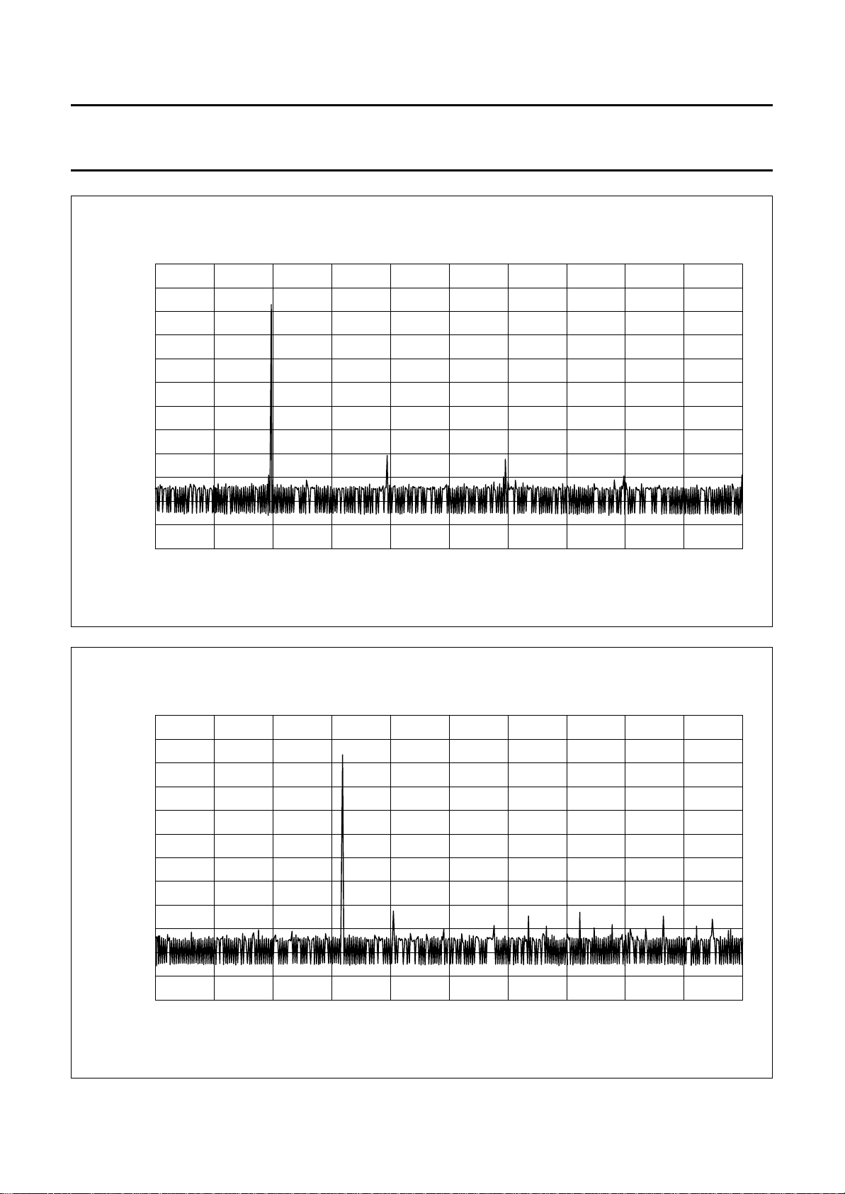
Fig.5 Typical output spectrum; f
= 500 MHz; f
clk
= 50 MHz.
OUT
f (MHz)
250
MGD472
−100
0 50 100 150 200
1996 Jun 04 9
Fig.6 Typical output spectrum; f
= 500 MHz; f
clk
= 80 MHz.
OUT
f (MHz)
250
Page 10
Philips Semiconductors Product specification
10-bit, 500 Msps Digital-to-Analog
Converter (DAC)
20
handbook, full pagewidth
DAC
OUTPUT
SPECTRUM
(dB)
0
−20
−40
−60
−80
−100
0 50 100 150 200
TDA8776
MGD473
f (MHz)
250
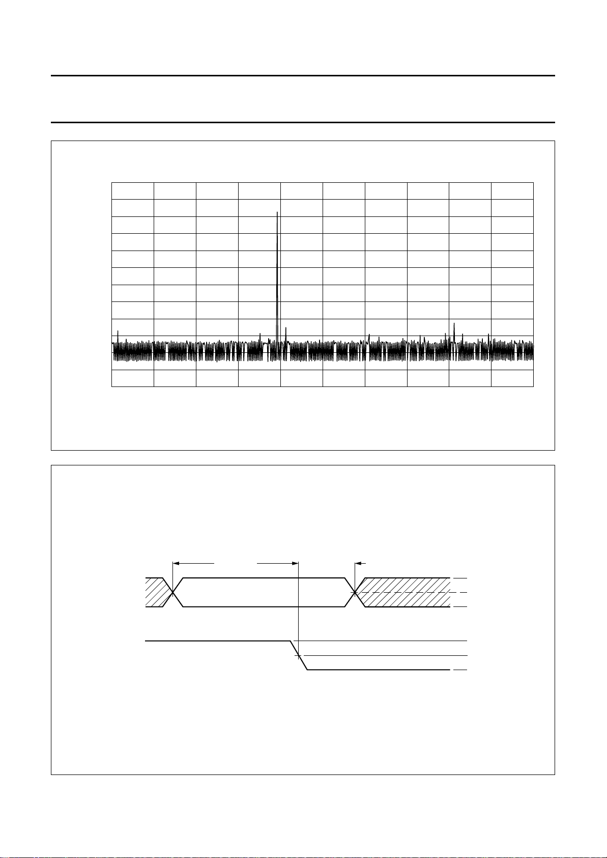
Fig.7 Typical output spectrum; f
t
handbook, full pagewidth
input data
CLK
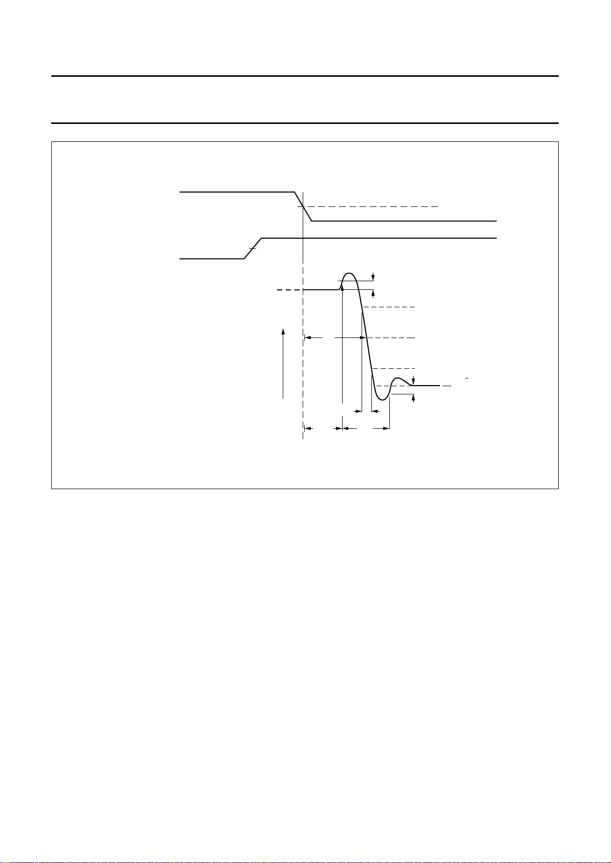
The shaded areas indicate when the input data may change and be correctly registered. Data input update must be completed within tbf ns after the
falling edge of the clock (t
is negative; tbf ns). Data must be held at least tbf ns after the falling edge (t
SU;DAT
SU; DAT
stable
= 500 MHz; f
clk
t
HD; DAT
= 100 MHz.
OUT
HD;DAT
MLD202
= tbfns).
0.9 V
1.35 V
1.8 V
0.9 V
1.35 V
1.8 V
1996 Jun 04 10
Fig.8 Data set-up and hold times.
Page 11
Philips Semiconductors Product specification
10-bit, 500 Msps Digital-to-Analog
Converter (DAC)
handbook, full pagewidth
CLK
input data
(example of a
full-scale input
transition)
code 0
1.35 V
0 V
(code 0)
V
OUT
TDA8776
1.35 V
code 1023
1 LSB
10 %
t
d
t
S1
t
PD
t
S2
50 %
90 %
1.0 V
(code 1023)
1 LSB
MLD203
Fig.9 Switching characteristics.
1996 Jun 04 11
Page 12
Philips Semiconductors Product specification
10-bit, 500 Msps Digital-to-Analog
Converter (DAC)
handbook, full pagewidth
V
OUT
HP80000
DATA
GENERATOR
V
OUT
f
clk /10
(2)
f
clk /10
(1)
f
clk
(3)
code 511
D9 MSB
D8
D7
D6
D5
D4
D3
D2
D1
D0 (LSB)
MODEL HP8133A
V
V
TDA8776
f
clk
PULSE
GENERATOR
(MASTER)
code 512
time
OUT
OUT
1 LSB
clock
(3)
(1)
(2)
TEK 11801A
20 GHz
SAMPLING
SCOPE
TDA8776
timing diagram
MLD204
The value of the glitch energy is the sum of the shaded areas measured in pV.s.
Fig.10 Glitch energy measurement.
1996 Jun 04 12
Page 13
Philips Semiconductors Product specification
10-bit, 500 Msps Digital-to-Analog
Converter (DAC)
INTERNAL PIN CONFIGURATIONS
IGND
handbook, 4 columns
D0 to D9
V
EEI
TDA8776
internal reference
MLD205
handbook, halfpage
AGND
V
OUT
V
OUT
V
EEA
MLD206
bit
n
switches and
current generators
Fig.11 D9 to D0.
50 Ω50 Ω
bit
n
DGND
lumns
V
CLK
EED
CLK
MLD207
Fig.12 Analog outputs.
1996 Jun 04 13
Fig.13 CLK and CLK.
Page 14
Philips Semiconductors Product specification
10-bit, 500 Msps Digital-to-Analog
Converter (DAC)
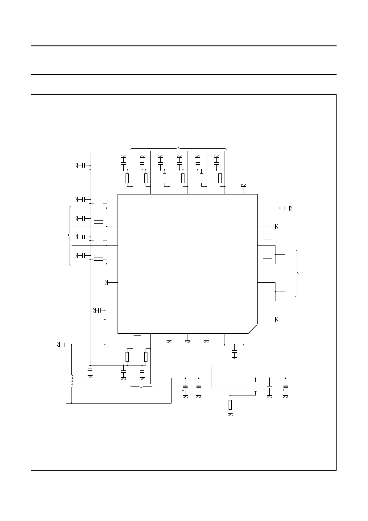
APPLICATION INFORMATION
handbook, full pagewidth
50 Ω digital
input matched
lines
1µF
10 nF
10 nF
10 nF
10 nF
V
TT
50 Ω
50 Ω
50 Ω
50 Ω
(1)
C
V
D6
D7
D8
D9
n.c.
EEA2
10
nF
50 Ω
10
nF
50 Ω
D5
18
19
20
21
22
23
24
17
50 Ω digital input matched lines
10
nF
50 Ω
D4
10
nF
16
50 Ω
D3
10
nF
50 Ω
D2
15
TDA8776
TDA8776
10
nF
50 Ω
D1
14
D0
IGND
13
12
V
EED3
11
AGND2
10
V
OUT2
9
V
OUT1
8
V
OUT2
7
V
OUT1
6
(1)
C
OUT
OUT
50 Ω analog
output matched
lines
VEE (−5.2 V)
22 µF
12
µH
1 µF
V
EEI
25
50 Ω
10
nF
26
50 Ω clock input
matched lines
CLK
50
10
nF
27
Ω
281234
22
µF
n.c.
1
µF
DGND1
LM337T
IN
CLK
DGND2
V
ADJ
EED1
75
Ω
C
OUT
(1)
V
EED2
AGND1
5
120
Ω
(1) C = 1 µF in parallel with 10 nF in parallel with 1 nF; all three mounted close to the supply pin of the DAC with 1 nF the nearest.
Fig.14 Application diagram.
1996 Jun 04 14
1
µF
VTT (−2 V)
22
µF
MBE379
Page 15
Philips Semiconductors Product specification
10-bit, 500 Msps Digital-to-Analog
Converter (DAC)
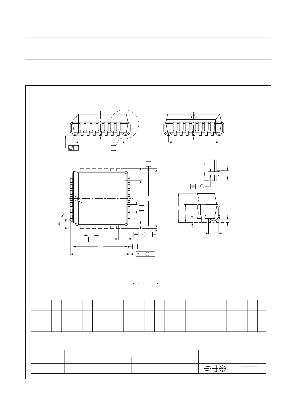
PACKAGE OUTLINE
PLCC28: plastic leaded chip carrier; 28 leads
e
y
25
26
28
1
pin 1 index
4
β
k
511
E
X
19
e
Z
D
H
D
TDA8776
SOT261-2
e
E
A
Z
E
18
H
E
E
e
12
k
1
v M
A
A
A
1
A
4
D
B
v M
B
w M
detail X
b
p
b
1
(A )
3
L
p
DIMENSIONS (millimetre dimensions are derived from the original inch dimensions)
A
UNIT A
mm
inches
0.180
0.165
1
A
min. max. max. max. max.
4.57
0.51
0.020
0.25
0.01
4.19
Note
1. Plastic or metal protrusions of 0.01 inches maximum per side are not included.
OUTLINE
VERSION
SOT261-2
1996 Jun 04 15
0 5 10 mm
A
4
3
3.05
0.12
b
0.53
0.33
0.021
0.013
b
p
1
0.81
0.66
0.032
0.026
(1)
D
11.58
11.43
0.456
0.450
(1)
E
eH
11.58
1.27
11.43
0.456
0.05
0.450
REFERENCES
IEC JEDEC EIAJ
e
D
10.92
9.91
0.430
0.390
scale
e
10.92
9.91
0.430
0.390
k
H
E
D
E
12.57
12.57
12.32
12.32
0.495
0.495
0.485
0.485
k
1.22
1.07
0.048
0.042
0.51
0.020
1
L
p
1.44
1.02
0.057
0.040
0.18 0.100.18
0.007 0.0040.007
EUROPEAN
PROJECTION
(1) (1)
Z
Z
E
D
ywv β
2.16
2.16
o
45
0.085
0.085
ISSUE DATE
92-11-17
95-02-25
Page 16

Philips Semiconductors Product specification
10-bit, 500 Msps Digital-to-Analog
Converter (DAC)
SOLDERING
Introduction
There is no soldering method that is ideal for all IC
packages. Wave soldering is often preferred when
through-hole and surface mounted components are mixed
on one printed-circuit board. However, wave soldering is
not always suitable for surface mounted ICs, or for
printed-circuits with high population densities. In these
situations reflow soldering is often used.
This text gives a very brief insight to a complex technology.
A more in-depth account of soldering ICs can be found in
“IC Package Databook”
our
Reflow soldering
Reflow soldering techniques are suitable for all PLCC
packages.
The choice of heating method may be influenced by larger
PLCC packages (44 leads, or more). If infrared or vapour
phase heating is used and the large packages are not
absolutely dry (less than 0.1% moisture content by
weight), vaporization of the small amount of moisture in
them can cause cracking of the plastic body. For more
information, refer to the Drypack chapter in our
Reference Handbook”
Reflow soldering requires solder paste (a suspension of
fine solder particles, flux and binding agent) to be applied
to the printed-circuit board by screen printing, stencilling or
pressure-syringe dispensing before package placement.
Several techniques exist for reflowing; for example,
thermal conduction by heated belt. Dwell times vary
between 50 and 300 seconds depending on heating
method. Typical reflow temperatures range from
215 to 250 °C.
(order code 9398 652 90011).
“Quality
(order code 9397 750 00192).
TDA8776
Wave soldering
Wave soldering techniques can be used for all PLCC
packages if the following conditions are observed:
• A double-wave (a turbulent wave with high upward
pressure followed by a smooth laminar wave) soldering
technique should be used.
• The longitudinal axis of the package footprint must be
parallel to the solder flow.
• The package footprint must incorporate solder thieves at
the downstream corners.
During placement and before soldering, the package must
be fixed with a droplet of adhesive. The adhesive can be
applied by screen printing, pin transfer or syringe
dispensing. The package can be soldered after the
adhesive is cured.
Maximum permissible solder temperature is 260 °C, and
maximum duration of package immersion in solder is
10 seconds, if cooled to less than 150 °C within
6 seconds. Typical dwell time is 4 seconds at 250 °C.
A mildly-activated flux will eliminate the need for removal
of corrosive residues in most applications.
Repairing soldered joints
Fix the component by first soldering two diagonallyopposite end leads. Use only a low voltage soldering iron
(less than 24 V) applied to the flat part of the lead. Contact
time must be limited to 10 seconds at up to 300 °C. When
using a dedicated tool, all other leads can be soldered in
one operation within 2 to 5 seconds between
270 and 320 °C.
Preheating is necessary to dry the paste and evaporate
the binding agent. Preheating duration: 45 minutes at
45 °C.
1996 Jun 04 16
Page 17

Philips Semiconductors Product specification
10-bit, 500 Msps Digital-to-Analog
TDA8776
Converter (DAC)
DEFINITIONS
Data sheet status
Objective specification This data sheet contains target or goal specifications for product development.
Preliminary specification This data sheet contains preliminary data; supplementary data may be published later.
Product specification This data sheet contains final product specifications.
Limiting values
Limiting values given are in accordance with the Absolute Maximum Rating System (IEC 134). Stress above one or
more of the limiting values may cause permanent damage to the device. These are stress ratings only and operation
of the device at these or at any other conditions above those given in the Characteristics sections of the specification
is not implied. Exposure to limiting values for extended periods may affect device reliability.
Application information
Where application information is given, it is advisory and does not form part of the specification.
LIFE SUPPORT APPLICATIONS
These products are not designed for use in life support appliances, devices, or systems where malfunction of these
products can reasonably be expected to result in personal injury. Philips customers using or selling these products for
use in such applications do so at their own risk and agree to fully indemnify Philips for any damages resulting from such
improper use or sale.
1996 Jun 04 17
 Loading...