

Page 1

INTEGRATED CIRCUITS
DATA SH EET
TDA8772; TDA8772A
Triple 8-bit video digital-to-analog
converter
Product specification
Supersedes data of May 1994
File under Integrated Circuits, IC02
Philips Semiconductors
1995 Mar 09
Page 2
Philips Semiconductors Product specification
Triple 8-bit video digital-to-analog
converter
FEATURES
• 8-bit resolution
• Sampling rate up to
35 MHz for TDA8772H/3, TDA8772AH/3
85 MHz for TDA8772H/8, TDA8772AH/8
• Internal reference voltage regulator
• No deglitching circuit required
• SYNC, BLANK control inputs
• 3 independent clock inputs (one per DAC)
• 1 V output voltage range
• 75 Ω output load
• TDA8772A has
channel only while TDA8772 has it on the 3 channels
• Single 5 V power supply
• 44-pin QFP package.
BLANK control input on the GREEN
TDA8772; TDA8772A
GENERAL DESCRIPTION
The TDA8772, TDA8772A are triple 8-bit video
digital-to-analog converters (DACs). They convert the
digital input signals into analog voltage outputs at a
maximum conversion rate of 35 MHz (TDA8772H/3,
TDA8772AH/3) and 85 MHz (TDA8772H/8,
TDA8772AH/8).
The DACs are based on resistor-string architecture with
integrated output buffers. The output voltage range is
determined by a built-in reference source.
The devices are fabricated in a 5 V CMOS process that
ensures high functionality with low power dissipation.
APPLICATIONS
• General purpose high-speed digital-to-analog
conversion
• Digital TV
• Graphic display
• Desktop video processing.
ORDERING INFORMATION
TYPE NUMBER
PACKAGE
PINS PIN POSITION MATERIAL CODE
TDA8772H/3 44 QFP44 plastic SOT307B 35 MHz
TDA8772AH/3 44 QFP44 plastic SOT307B 35 MHz
TDA8772H/8 44 QFP44 plastic SOT307B 85 MHz
TDA8772AH/8 44 QFP44 plastic SOT307B 85 MHz
SAMPLING
FREQUENCY
1995 Mar 09 2
Page 3

Philips Semiconductors Product specification
Triple 8-bit video digital-to-analog
TDA8772; TDA8772A
converter
QUICK REFERENCE DATA
SYMBOL PARAMETER CONDITIONS MIN. TYP. MAX. UNIT
V
DDA
V
DDD
I
DDA
I
DDD
INL integral non-linearity2 f
DNL differential non-linearity f
f
clk(max)
P
tot
analog supply voltage 4.5 5.0 5.5 V
digital supply voltage 4.5 5.0 5.5 V
analog supply current RL=75Ω; note 1 40 65 100 mA
digital supply current
TDA8772H/3, TDA8772AH/3 − 716mA
TDA8772H/8, TDA8772AH/8 − 16 27 mA
= 35 MHz; ramp input −±0.5 ±1 LSB
clk
f
= 85 MHz; ramp input −±0.75 ±1.2 LSB
clk
= 35 MHz; ramp input −±0.25 ±0.5 LSB
clk
= 85 MHz; ramp input - ±0.5 ±0.75 LSB
f
clk
maximum clock frequency
TDA8772H/3, TDA8772AH/3 35 −−MHz
TDA8772H/8, TDA8772AH/8 85 −−MHz
total power dissipation note 1
TDA8772H/3, TDA8772AH/3 R
TDA8772H/8, TDA8772AH/8 R
=75Ω; f
L
=75Ω; f
L
= 35 MHz 180 360 640 mW
clk
= 85 MHz 180 405 700 mW
clk
Note
1. Minimum and maximum data of current and power consumption are measured in worse case conditions: for
minimum data, all digital inputs are at logic level 0 while for maximum data, all digital inputs are at logic level 1.
1995 Mar 09 3
Page 4
Philips Semiconductors Product specification
Triple 8-bit video digital-to-analog
converter
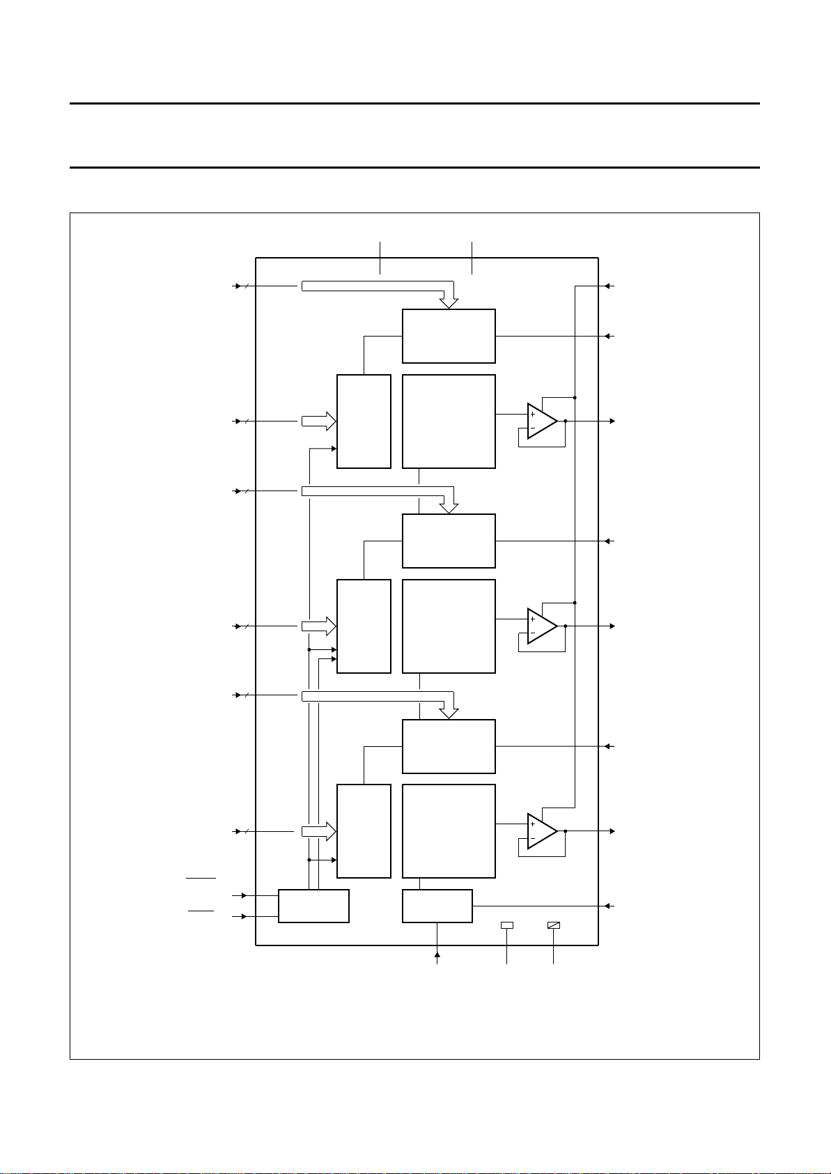
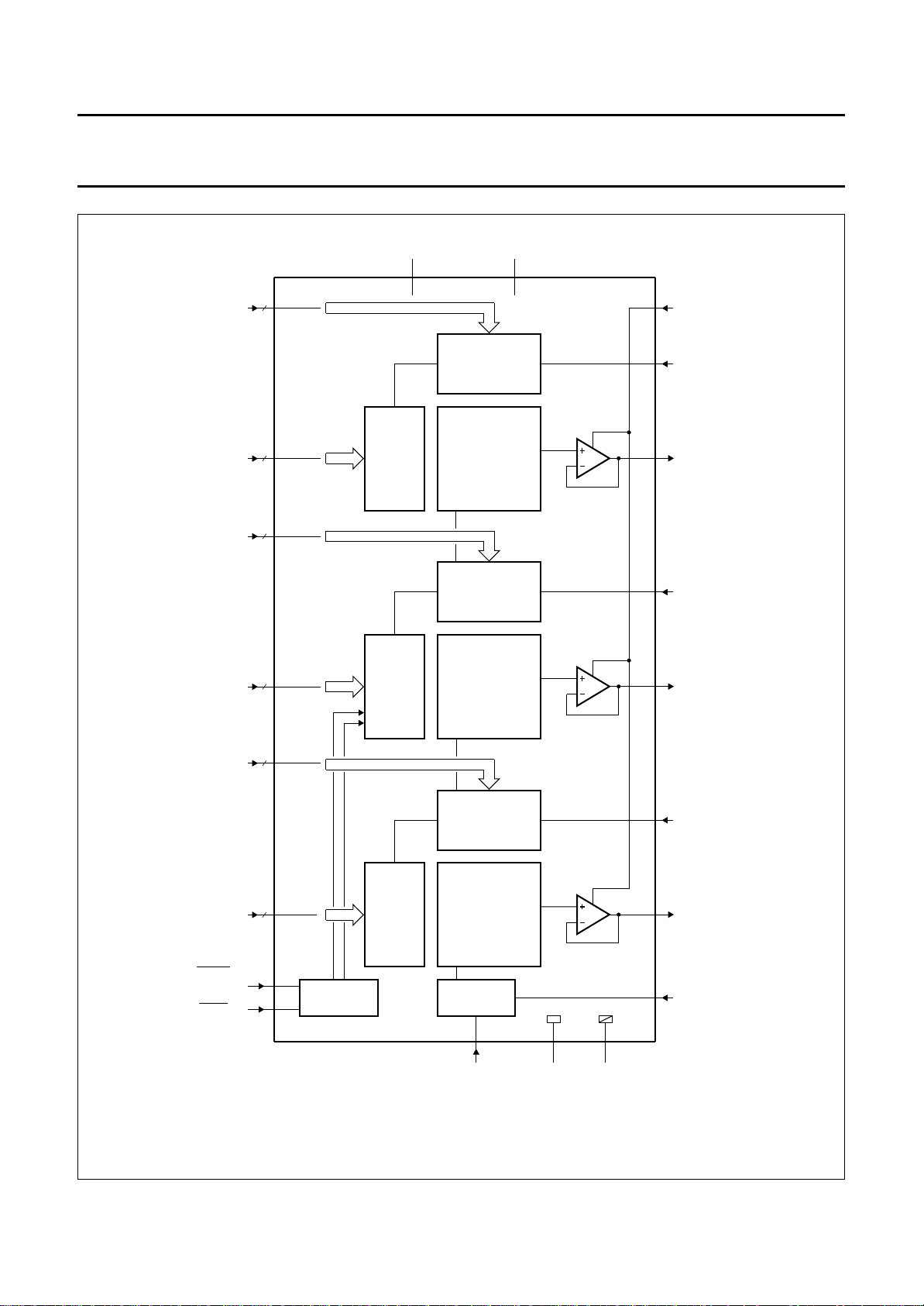
BLOCK DIAGRAMS
handbook, full pagewidth
RED
digital inputs
(bits R0 to R3)
RED
digital inputs
(bits R4 to R7)
GREEN
digital inputs
(bits G0 to G3)
4
8–5
TDA8772
4
4–1
4
20–17
4
V
DDA DDD
MSB
DECODER
V
4
LSB
DECODER
RESISTOR
STRING
4
TDA8772; TDA8772A
10,3235,39,43
41
21
44
reference
current input
(I )
REFB
RED
clock input
RED
analog output
GREEN
digital inputs
(bits G4 to G7)
BLUE
digital inputs
(bits B0 to B3)
BLUE
digital inputs
(bits B4 to B7)
BLANK
control input
SYNC
control input
4
4
16–13
31–284
27–24
12
11
4
4
CONTROL
REGISTER
MSB
DECODER
MSB
DECODER
LSB
DECODER
RESISTOR
STRING
4
LSB
DECODER
RESISTOR
STRING
BANDGAP
REFERENCE
34
37,42 9,33
22
40
23
36
38
GREEN
clock input
GREEN
analog output
BLUE
clock input
BLUE
analog output
reference current
input for internal
reference
(I )
REFA
1995 Mar 09 4
reference voltage
decoupling input
(V )
REF
V
SSA SSD
Fig.1 Block diagram for TDA8772.
V
MBB661 - 2
Page 5
Philips Semiconductors Product specification
Triple 8-bit video digital-to-analog
converter
handbook, full pagewidth
RED
digital inputs
(bits R0 to R3)
RED
digital inputs
(bits R4 to R7)
GREEN
digital inputs
(bits G0 to G3)
4
4
4
8–5
TDA8772A
4–1
20–17
4
MSB
DECODER
V
DDA DDD
V
4
LSB
DECODER
RESISTOR
STRING
4
LSB
DECODER
TDA8772; TDA8772A
10,3235,39,43
41
21
44
22
reference
current input
(I )
REFB
RED
clock input
RED
analog output
GREEN
clock input
GREEN
digital inputs
(bits G4 to G7)
BLUE
digital inputs
(bits B0 to B3)
BLUE
digital inputs
(bits B4 to B7)
BLANK
control input
SYNC
control input
4
4
16–13
31–284
27–24
12
11
4
4
CONTROL
REGISTER
MSB
DECODER
MSB
DECODER
RESISTOR
STRING
4
LSB
DECODER
RESISTOR
STRING
BANDGAP
REFERENCE
34
reference voltage
decoupling input
(V )
REF
37,42 9,33
V
V
SSA SSD
40
23
36
38
GREEN
analog output
BLUE
clock input
BLUE
analog output
reference current
input for internal
reference
(I )
REFA
MLB724
1995 Mar 09 5
Fig.2 Block diagram for TDA8772A.
Page 6
Philips Semiconductors Product specification
Triple 8-bit video digital-to-analog
TDA8772; TDA8772A
converter
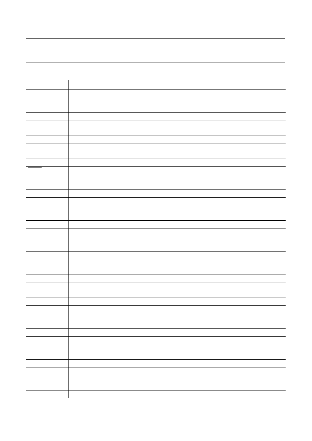
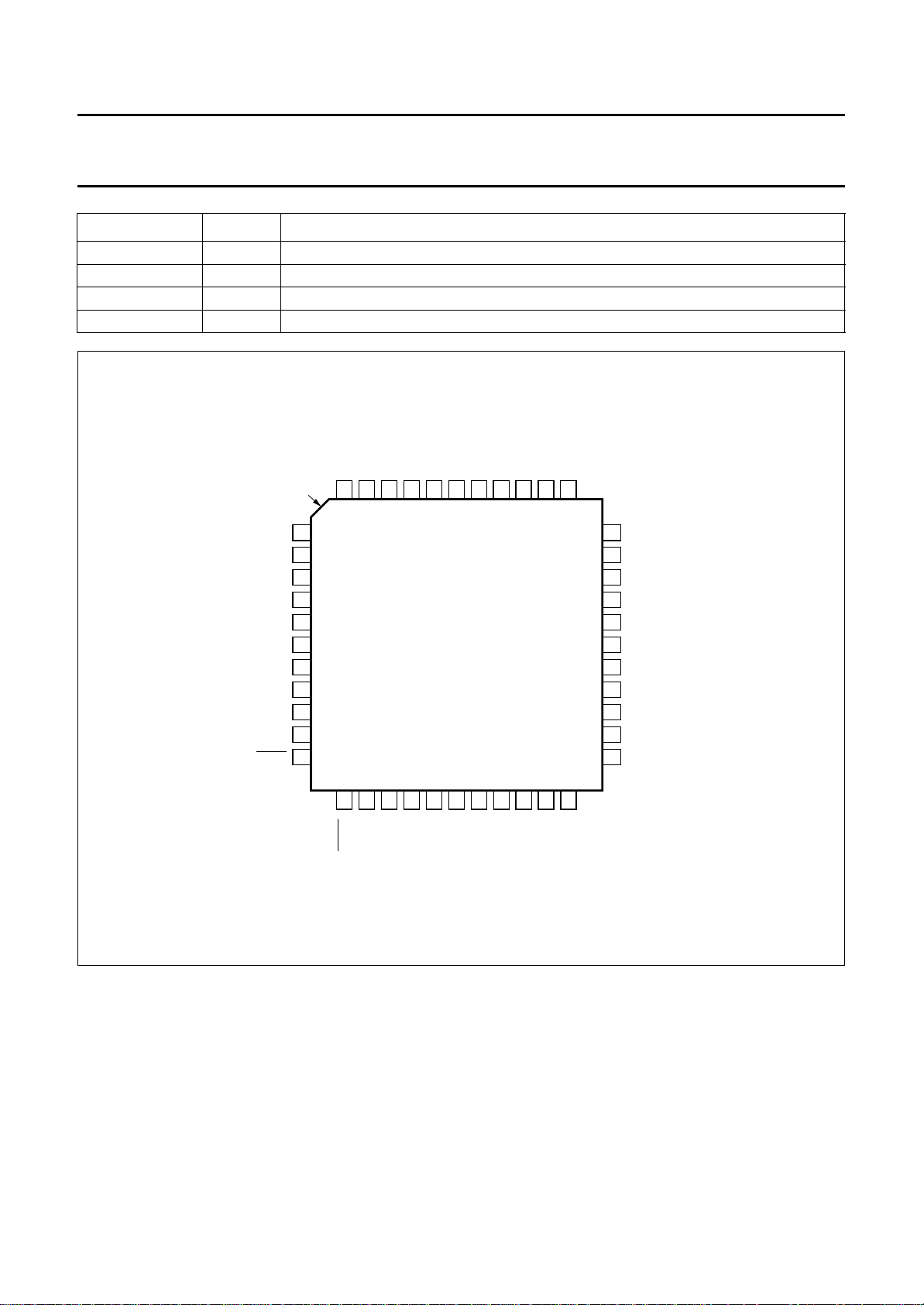
PINNING
SYMBOL PIN DESCRIPTION
R7 1 RED digital input data; bit 7 (MSB)
R6 2 RED digital input data; bit 6
R5 3 RED digital input data; bit 5
R4 4 RED digital input data; bit 4
R3 5 RED digital input data; bit 3
R2 6 RED digital input data; bit 2
R1 7 RED digital input data; bit 1
R0 8 RED digital input data; bit 0 (LSB)
V
SSD1
V
DDD1
SYNC 11 composite sync control input; for GREEN channel only (active LOW)
BLANK 12 composite blank control input (active LOW)
G7 13 GREEN digital input data; bit 7 (MSB)
G6 14 GREEN digital input data; bit 6
G5 15 GREEN digital input data; bit 5
G4 16 GREEN digital input data; bit 4
G3 17 GREEN digital input data; bit 3
G2 18 GREEN digital input data; bit 2
G1 19 GREEN digital input data; bit 1
G0 20 GREEN digital input data; bit 0 (LSB)
CLKR 21 RED clock input
CLKG 22 GREEN clock input
CLKB 23 BLUE clock input
B7 24 BLUE digital input data; bit 7 (MSB)
B6 25 BLUE digital input data; bit 6
B5 26 BLUE digital input data; bit 5
B4 27 BLUE digital input data; bit 4
B3 28 BLUE digital input data; bit 3
B2 29 BLUE digital input data; bit 2
B1 30 BLUE digital input data; bit 1
B0 31 BLUE digital input data; bit 0 (LSB)
V
DDD2
V
SSD2
V
REF
V
DDA1
OUTB 36 BLUE analog output
V
SSA1
I
REFA
V
DDA2
OUTG 40 GREEN analog output
9 digital supply ground 1
10 digital supply voltage 1
32 digital supply voltage 2
33 digital supply ground 2
34 decoupling input for reference voltage
35 analog supply voltage 1
37 analog supply ground 1
38 reference current input for internal reference
39 analog supply voltage 2
1995 Mar 09 6
Page 7
Philips Semiconductors Product specification
Triple 8-bit video digital-to-analog
converter
SYMBOL PIN DESCRIPTION
I
REFB
V
SSA2
V
DDA3
OUTR 44 RED analog output
handbook, full pagewidth
41 reference current input for output buffers
42 analog supply ground 2
43 analog supply voltage 3
V
SSD1
V
DDD1
SYNC
index
corner
R7
R6
R5
R4
R3
R2
R1
R0
DDA3
SSA2
V
V
OUTR
44
1
2
3
4
5
6
7
8
9
10
11
I
41
43
42
REFB
OUTG
V
40
39
TDA8772
TDA8772A
DDA2
REFA
I
38
SSA1
V
37
OUTB
36
V
DDA1
35
REF
V
34
TDA8772; TDA8772A
V
33
SSD2
V
32
DDD2
31
B0
30
B1
29
B2
B3
28
27
B4
26
B5
25
B6
B7
24
23
CLKB
12
13
14
15
16
G5
G6
G4
G7
BLANK
Fig.3 Pin configuration.
1995 Mar 09 7
17
G3
18
G2
19
G1
20
G0
21
CLKR
22
CLKG
MBB660 - 3
Page 8
Philips Semiconductors Product specification
Triple 8-bit video digital-to-analog
TDA8772; TDA8772A
converter
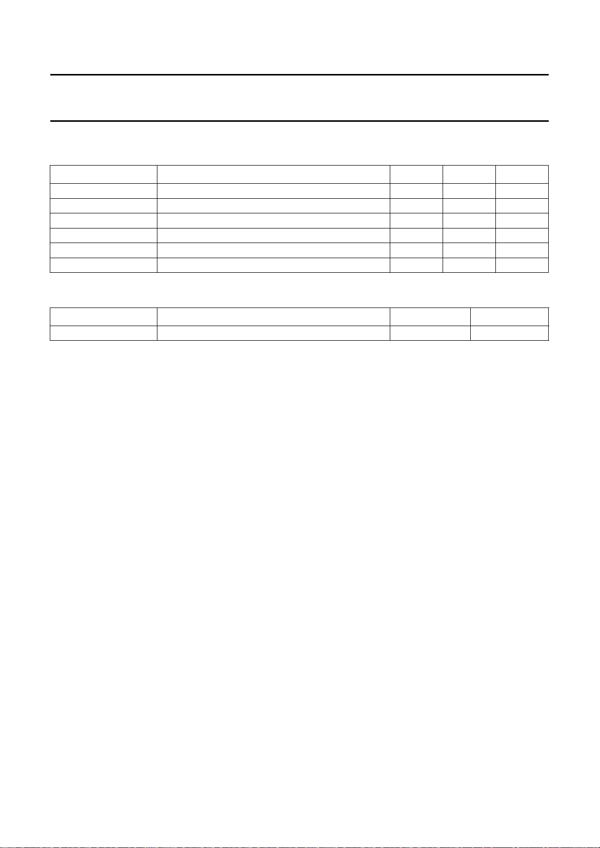
LIMITING VALUES
In accordance with the Absolute Maximum Rating System (IEC134).
SYMBOL PARAMETER MIN. MAX. UNIT
V
DDA
V
DDD
∆V
DD
T
stg
T
amb
T
j
THERMAL CHARACTERISTICS
SYMBOL PARAMETER VALUE UNIT
R
th j-a
HANDLING
Inputs and outputs are protected against electrostatic discharges in normal handling. However, to be totally safe, it is
desirable to take normal precautions appropriate to handling integrated circuits.
analog supply voltage −0.5 +6.5 V
digital supply voltage −0.5 +6.5 V
supply voltage difference between V
DDA
and V
DDD
−1.0 +1.0 V
storage temperature −55 +150 °C
operating ambient temperature 0 +70 °C
junction temperature − +125 °C
thermal resistance from junction to ambient in free air 75 K/W
1995 Mar 09 8
Page 9
Philips Semiconductors Product specification
Triple 8-bit video digital-to-analog
TDA8772; TDA8772A
converter
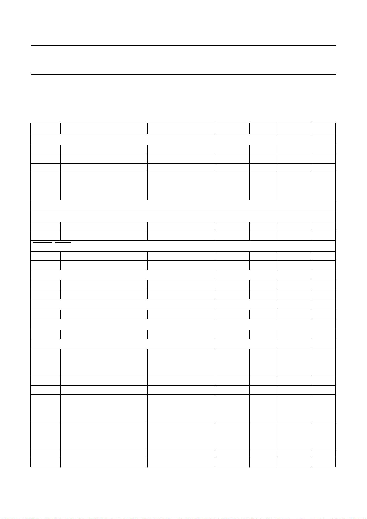
CHARACTERISTICS
TDA8772H/3, TDA8772AH/3 operating at 35 MHz and TDA8772H/8, TDA8772AH/8 operating at 85 MHz unless
otherwise specified.
V
DDA=VDDD
typical values measured at V
SYMBOL PARAMETER CONDITIONS MIN. TYP. MAX. UNIT
Supply
V
DDA
V
DDD
I
DDA
I
DDD
Inputs
LOCK INPUTS (PINS 21, 22 AND 23)
C
V
IL
V
IH
BLANK, SYNC INPUTS (PINS 12 AND 11; ACTIVE LOW)
V
IL
V
IH
R, G, B DIGITAL INPUTS (PINS 1 TO 8, 13 TO 20 AND 24 TO 31)
V
IL
V
IH
I
REFA
I
I
I
REFB
I
I
Timing (CL= 25 pF; RL=75Ω); see Fig.4
f
clk(max)
t
CPH
t
CPL
t
r
t
f
t
SU;DAT
t
HD;DAT
= 4.5 V to 5.5 V; V
and V
SSA
DDA=VDDD
shorted together; V
SSD
= 5 V and T
amb
DDA
− V
= −0.5 V to +0.5 V; T
DDD
=25°C; unless otherwise specified.
amb
analog supply voltage 4.5 5.0 5.5 V
digital supply voltage 4.5 5.0 5.5 V
analog supply current RL=75Ω; note 1 40 65 100 mA
digital supply current
TDA8772H/3, TDA8772AH/3 − 716 mA
TDA8772H/8, TDA8772AH/8 − 16 27 mA
LOW level input voltage V
HIGH level input voltage 2.0 − V
LOW level input voltage V
HIGH level input voltage 2.0 − V
LOW level input voltage V
HIGH level input voltage 2.0 − V
INTERNAL REFERENCE SUPPLY CURRENT (PIN 38)
− 0.5 − 0.8 V
SSD
DDD
− 0.5 − 0.8 V
SSD
DDD
− 0.5 − 0.8 V
SSD
DDD
input current − 0.17 0.25 mA
OUTPUT BUFFER SUPPLY CURRENT (PIN 41)
input current − 0.5 0.7 mA
maximum clock frequency
TDA8772H/3, TDA8772AH/3 35 −− MHz
TDA8772H/8, TDA8772AH/8 85 −− MHz
clock pulse width HIGH 5 −− ns
clock pulse width LOW 5 −− ns
clock rise time
TDA8772H/3, TDA8772AH/3 −−5ns
TDA8772H/8, TDA8772AH/8 −−3ns
clock fall time
TDA8772H/3, TDA8772AH/3 −−5ns
TDA8772H/8, TDA8772AH/8 −−3ns
input data set-up time 4 −− ns
input data hold time 2.5 −− ns
= 0 to +70 °C;
+ 0.5 V
+ 0.5 V
+ 0.5 V
1995 Mar 09 9
Page 10
Philips Semiconductors Product specification
Triple 8-bit video digital-to-analog
TDA8772; TDA8772A
converter
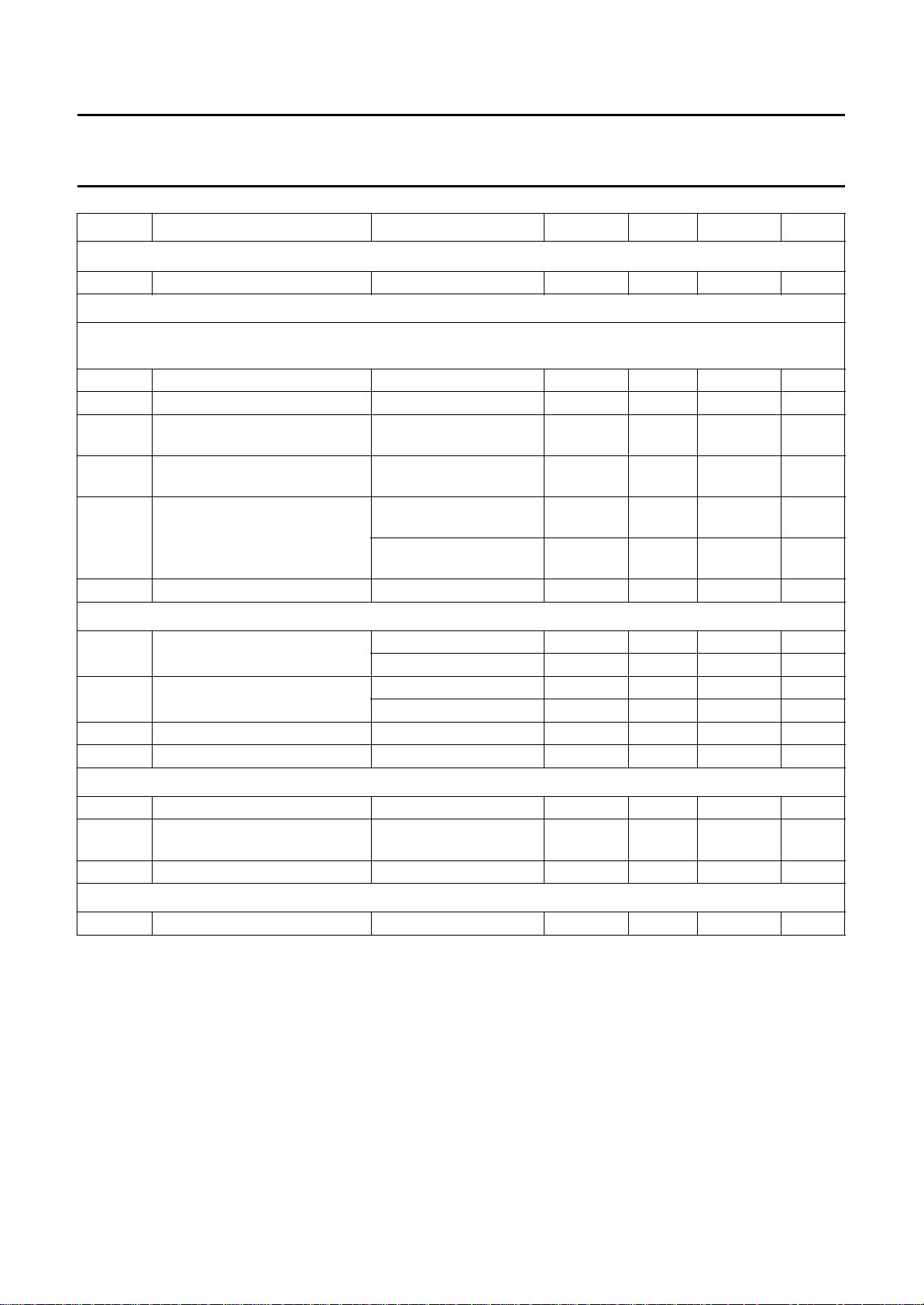
SYMBOL PARAMETER CONDITIONS MIN. TYP. MAX. UNIT
Voltage reference (pin 34, referenced to V
V
REF
output reference voltage 1.180 1.242 1.305 V
Outputs
OUTB, OUTR, OUTG
ANALOG OUTPUTS (PINS 36, 44 AND 40, REFERENCED TO V
see Tables 1 and 2
FSR full-scale output voltage range 0.9 1.0 1.1 V
V
os
V
OUTmax
V
OUTmin
offset of analog voltage output 0.75 0.83 0.95 V
maximum output voltage data inputs = logic 1;
minimum output voltage data inputs = logic 0;
THD total harmonic distortion f
Z
L
output load impedance 60 75 90 Ω
Transfer function
INL integral non-linearity f
DNL differential non-linearity f
α
CT
crosstalk DAC to DAC −45 −− dB
DAC to DAC matching − 1.0 2.0 %
)
SSA
) FOR 75 Ω LOAD;
SSA
1.65 1.83 2.05 V
note 2
0.75 0.83 0.95 V
note 2
= 4.43 MHz;
i
f
=35MHz
clk
f
= 4.43 MHz;
i
f
=85MHz
clk
= 35 MHz; ramp input −±0.5 ±1 LSB
clk
= 85 MHz; ramp input −±0.75 ±1.2 LSB
f
clk
= 35 MHz; ramp input −±0.25 ±0.5 LSB
clk
= 85 MHz; ramp input - ±0.5 ±0.75 LSB
f
clk
−−45 − dB
−−43 − dB
Switching characteristics (for 75 Ω output load); see Fig.5
t
d
t
s1
input to 50% output delay time full-scale change − 10 − ns
settling time 10% to 90% full-scale
− 6 − ns
change
t
s2
settling time to ±1 LSB − 30 − ns
Output transients (glitches)
V
g
area for 1 LSB change − 1 − LSB.ns
Notes
1. Minimum and maximum data of current and power consumption are measured in worse case conditions: for
minimum data, all digital inputs are at logic level 0 while for maximum data, all digital inputs are at logic level 1.
2. V
is directly proportional to V
OUT
REF
.
1995 Mar 09 10
Page 11
Philips Semiconductors Product specification
Triple 8-bit video digital-to-analog
converter
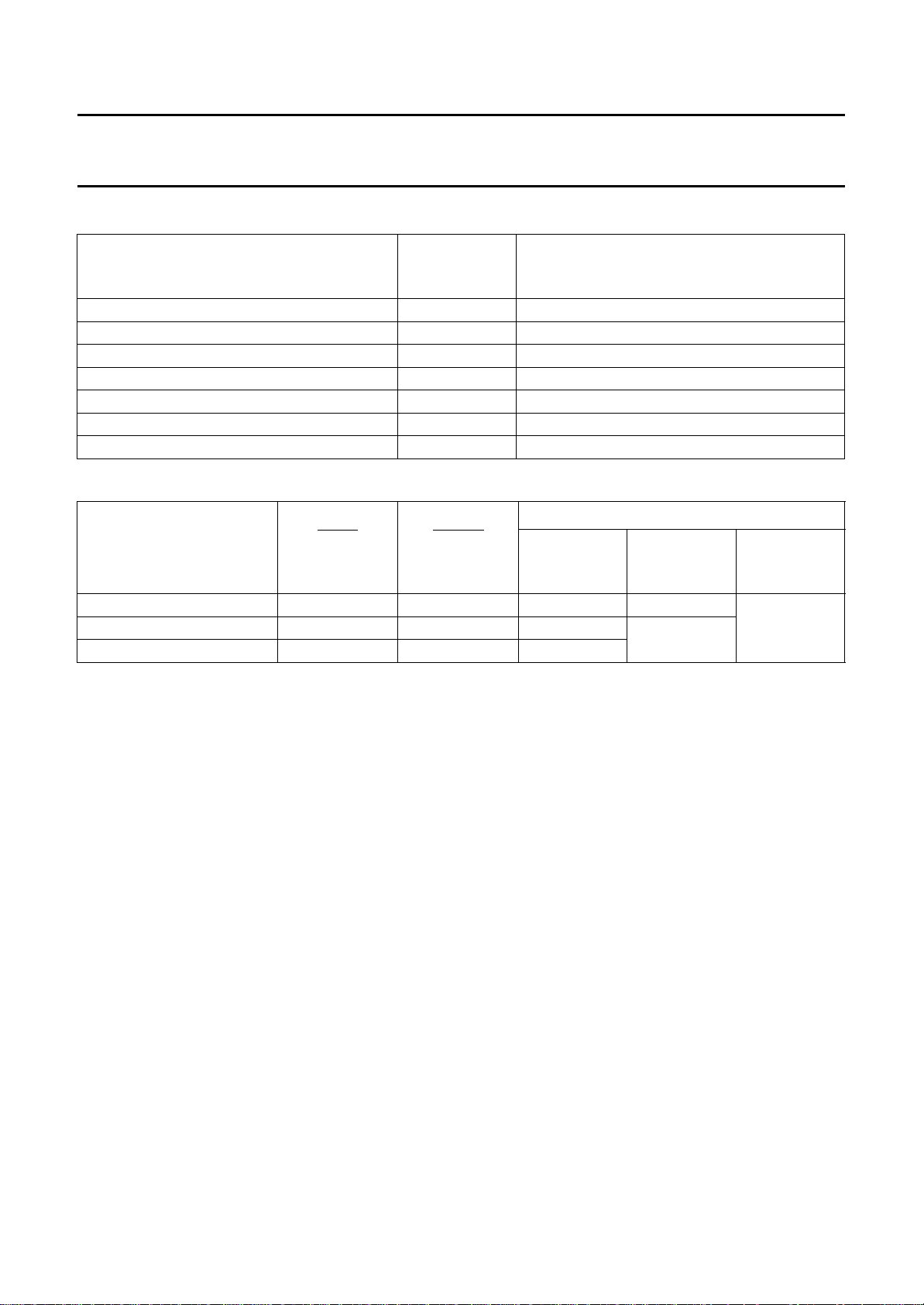
Table 1 Input coding and DAC output voltages (typical values)
BINARY INPUT DATA
(SYNC = BLANK = 0)
0000 0000 0 0.830
0000 0001 1 0.834
.... .... . .
1000 0000 128 1.330
.... .... . .
1111 1110 254 1.826
1111 1111 255 1.830
Table 2 Input coding and DAC output voltages (typical values)
BINARY INPUT DATA
.... .... x 1 see Table 1 see Table 1
.... .... 0 0 0.440
SYNC
(PIN 11)
CODE
BLANK
(PIN 12)
TDA8772; TDA8772A
DAC OUTPUT VOLTAGES (V)
OUTB, OUTR, OUTG
RL=75Ω
DAC OUTPUT VOLTAGES (V)
OUTG
(PIN 40)
OUTR/B
(PINS 44, 46)
TDA8772
0.830
OUTR/B
(PINS 44, 46)
TDA8772A
see Table 1.... .... 1 0 0.830
1995 Mar 09 11
Page 12
Philips Semiconductors Product specification
Triple 8-bit video digital-to-analog
converter
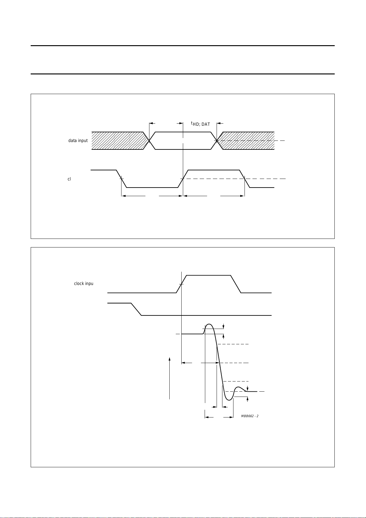
TIMING
ndbook, full pagewidth
data input
clock input
t
SU; DAT
stable
t
CPL
Fig.4 Input timing.
t
HD; DAT
t
CPH
TDA8772; TDA8772A
V
IH
50 %
V
IL
50 %
V
MBB656 - 1
IL
handbook, full pagewidth
clock input
input code
(example of a
full-scale input
data transition)
code 255
50 %
1.83 V
(code 255)
V
o
code 0
1 LSB
10 %
t
d
t
s1
t
s2
50 %
90 %
1 LSB
MBB662 - 2
0.83 V
(code 0)
1995 Mar 09 12
Fig.5 Switching timing.
Page 13
Philips Semiconductors Product specification
Triple 8-bit video digital-to-analog
converter
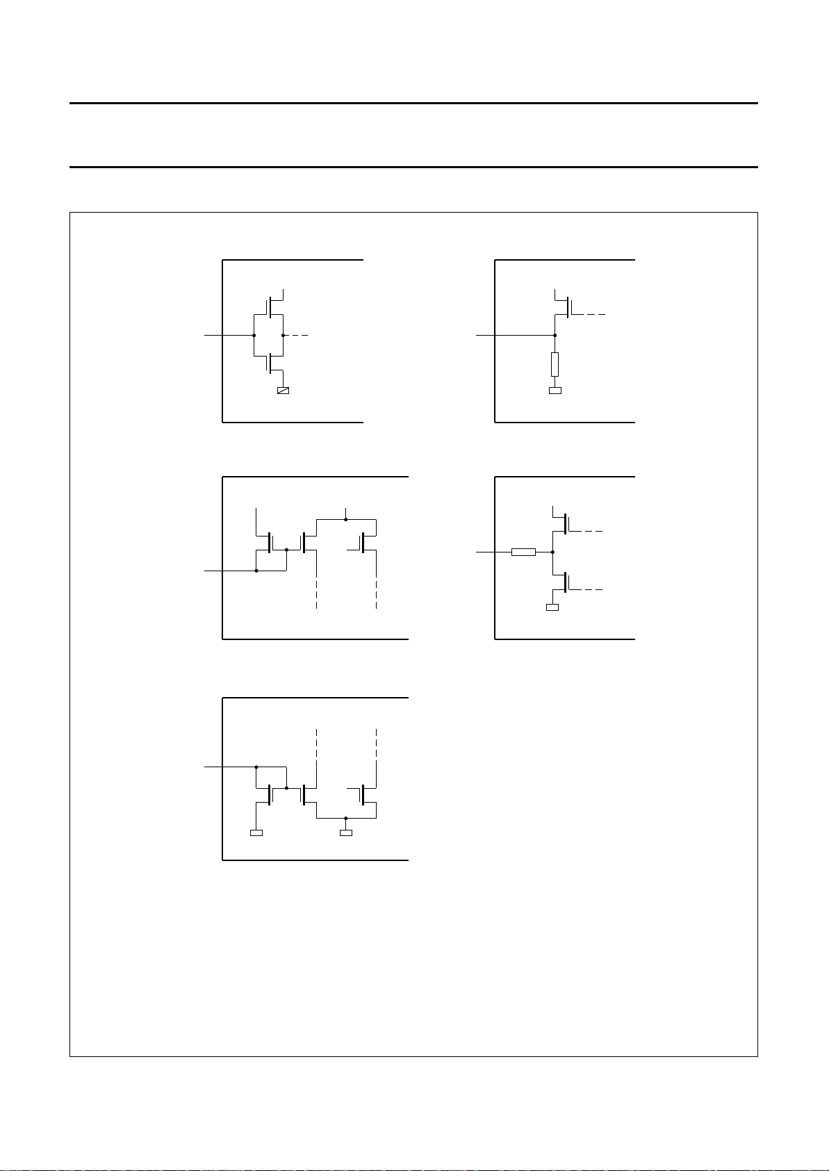
INTERNAL CIRCUITRY
handbook, full pagewidth
V
DDD
GND
V
SSD
(a)
V
DDA
V
DD
V
V
DD
DDA
TDA8772; TDA8772A
V
DDA
DACs
resistor
string
V
SSA
(b)
V
DDA
V
DD
V
DD
25 Ω
(typ)
GND
GND GND GND
V
SSA
(a) Digital inputs; pins 1to 8 and 11to 31.
(b) VREF; pin 34.
(c) IREFA; pin 38.
(d) OUTR, G, B; pins 44, 40 and 36.
(e) IREFB; pin 41.
(c)
(e)
V
SSA
MBB663 - 2
V
SSA
(d)
1995 Mar 09 13
Fig.6 Internal circuitry.
Page 14
Philips Semiconductors Product specification
Triple 8-bit video digital-to-analog
converter
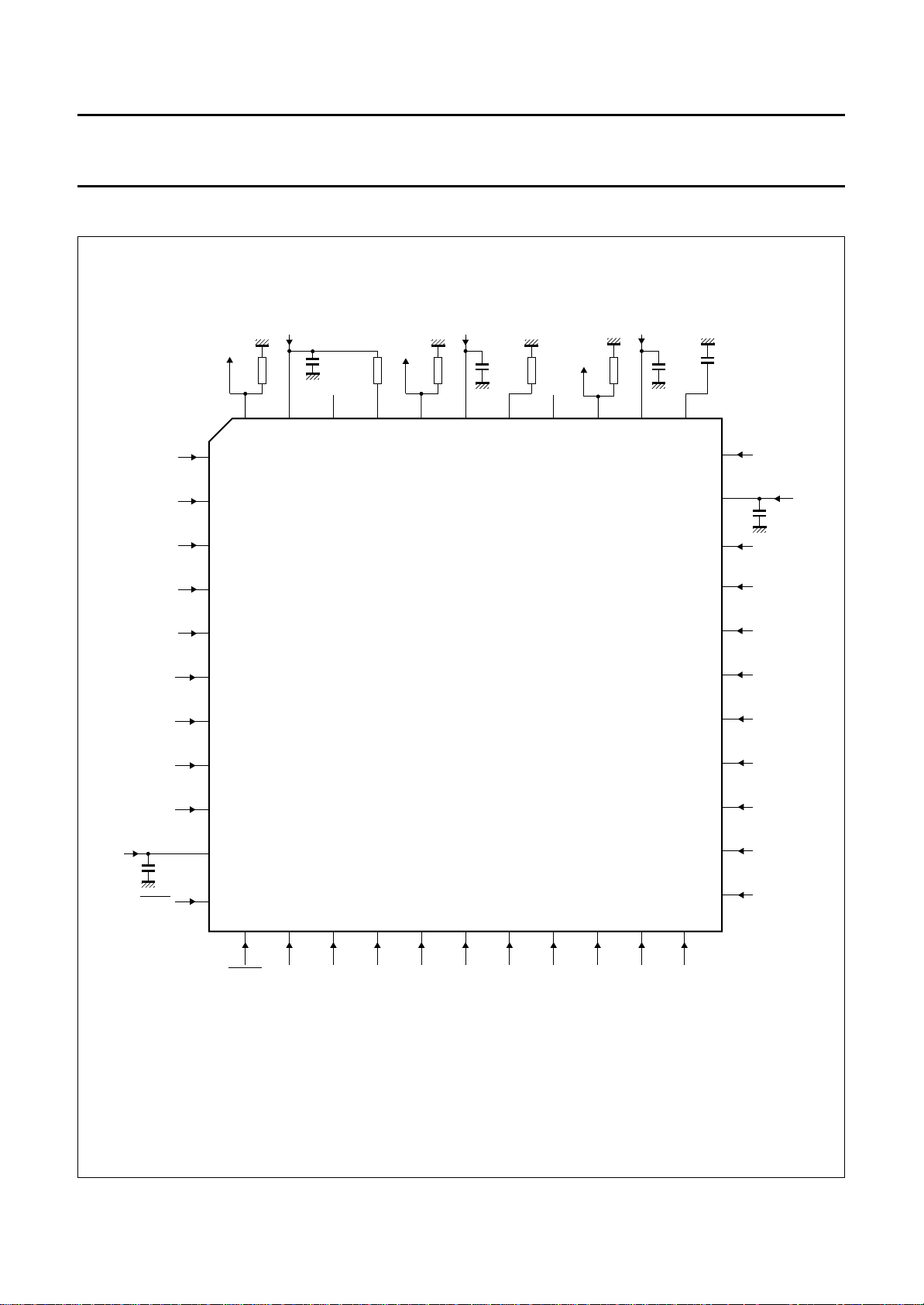
APPLICATION INFORMATION
handbook, full pagewidth
R7
R6
R5
R4
OUTR
1
2
3
4
5 V
V
SSA
V
DDA3
10 nF
V
SSA
V
SSA2
75
Ω
44 43 42 41 40 39 38 37 36 35 34
OUTG
8.2
kΩ
IREFB
V
SSA
OUTG
TDA8772; TDA8772A
V
OUTB
SSA1
V
SSA
5 V
75
Ω
5 V
75
Ω
V
10
nF
V
DDA2
SSA
V
SSA
IREFA
33
kΩ
V
DDA1
10
nF
V
SSA
V
V
SSA
REF
33
32
31
30
100 nF
V
DDD2
V
B0
B1
SSD2
10 nF
V
SSD
5 V
R3
R2
R1
R0
V
SSD1
V
5 V
V
SSD
Analog and digital supplies should be separated and decoupled.
Supplies are not connected internally.
All ground pins must be connected. One ground plane is preferred although it depends on the application.
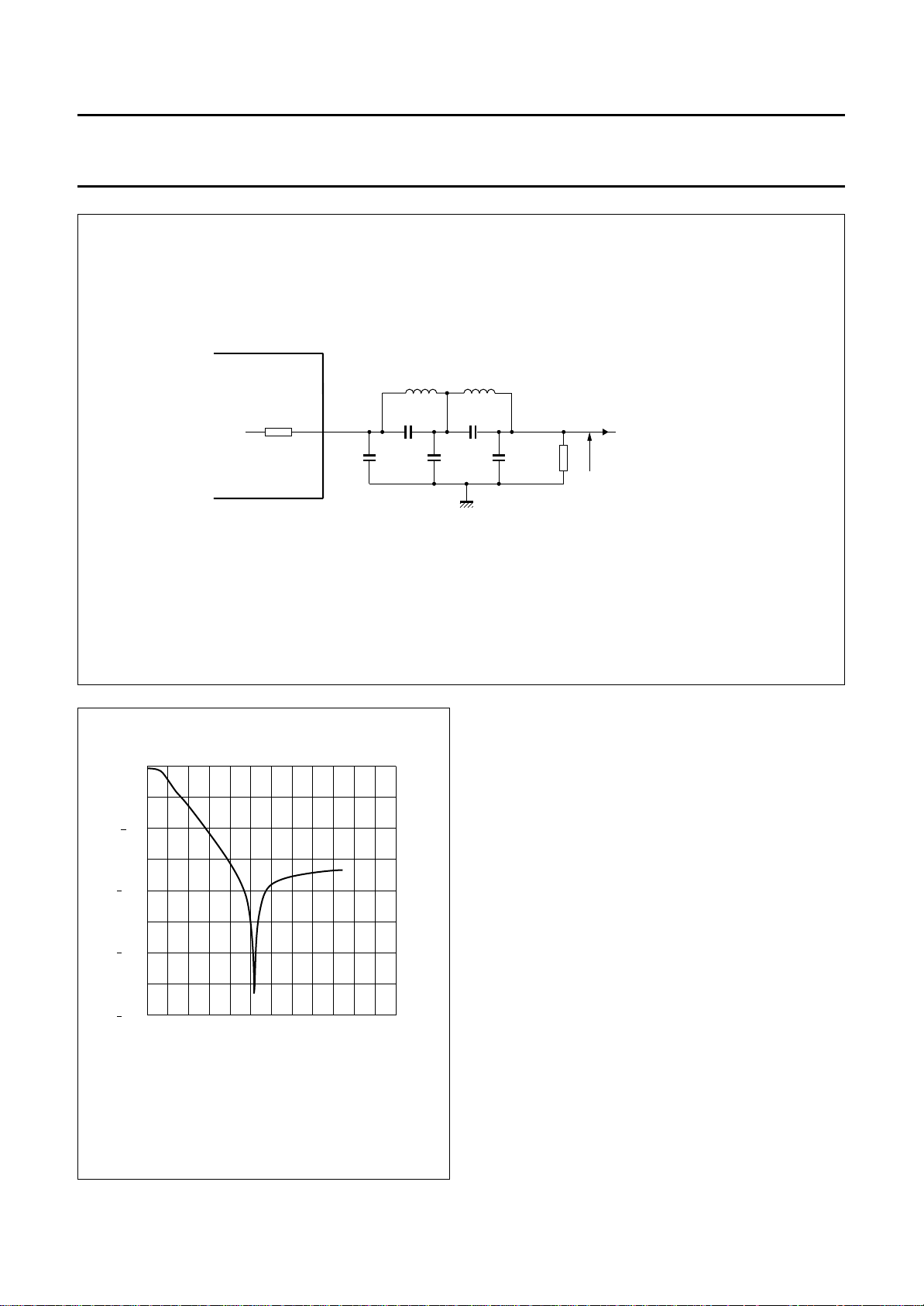
See Fig.8 for example of anti-aliasing filter.
DDD1
10 nF
SYNC
5
6
7
8
9
10
11
12 13 14 15 16 17 18 19 20 21 22
BLANK G7 G6 G5 G4 G3 G2 G1 G0 CLKR
TDA8772
TDA8772A
CLKG
29
28
27
26
25
24
23
B2
B3
B4
B5
B6
B7
CLKB
MBB664 - 4
1995 Mar 09 14
Fig.7 Application diagram.
Page 15
Philips Semiconductors Product specification
Triple 8-bit video digital-to-analog
converter
handbook, full pagewidth
TDA8772
TDA8772A
Ω25
OUTR (pin 44)
and OUTG (pin 40)
and OUTB (pin 36)
220 pF 1.5 nF 220 pF
1 µH1 µH
12 pF 12 pF
analog ground
75 Ω
MSA692 - 1
TDA8772; TDA8772A
analog video output
(R,G or B)
1 V (p-p)
handbook, halfpage
0
α
(dB)
50
100
150
200
0 36 108
Fig.8 Example of anti-aliasing filter for 1 V output swing.
Characteristics of Fig.9
• Order 5; adapted CHEBYSHEV
MSA691
• Ripple ρ≥0.6 dB
• fat−3 dB = 6.5 MHz
72
• f
f (MHz)
NOTCH
= 46 MHz.
Fig.9 Frequency response for filter shown in Fig.8.
1995 Mar 09 15
Page 16
Philips Semiconductors Product specification
Triple 8-bit video digital-to-analog
TDA8772; TDA8772A
converter
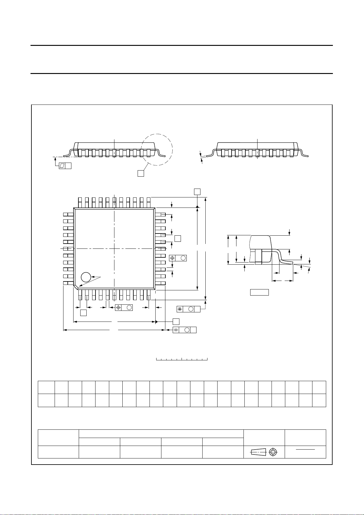
PACKAGE OUTLINE
QFP44: plastic quad flat package; 44 leads (lead length 1.3 mm); body 10 x 10 x 1.75 mm
c
y
X
A
33 23
34
22
Z
E
SOT307-2
e
w
M
b
p
pin 1 index
44
1
w
H
0.40
0.20
M
D
D
D
0.25
10.1
0.14
9.9
b
e
DIMENSIONS (mm are the original dimensions)
mm
A
max.
2.10
0.25
0.05
1.85
1.65
UNIT A1A2A3bpcE
Note
1. Plastic or metal protrusions of 0.25 mm maximum per side are not included.
p
0.25
12
11
Z
D
B
v
0 2.5 5 mm
scale
(1)
(1) (1)(1)
eH
H
10.1
9.9
12.9
0.8 1.3
12.3
D
v
M
E
M
A
B
E
12.9
12.3
H
E
LLpQZywv θ
0.95
0.55
A
2
A
A
1
detail X
0.85
0.75
0.15 0.10.15
Q
(A )
3
θ
L
p
L
Z
E
D
1.2
0.8
1.2
0.8
o
10
o
0
OUTLINE
VERSION
SOT307-2
1995 Mar 09 16
REFERENCES
IEC JEDEC EIAJ
EUROPEAN
PROJECTION
ISSUE DATE
92-11-17
95-02-04
Page 17

Philips Semiconductors Product specification
Triple 8-bit video digital-to-analog
converter
SOLDERING
Plastic quad flat packages
YWAVE
B
During placement and before soldering, the component
must be fixed with a droplet of adhesive. After curing the
adhesive, the component can be soldered. The adhesive
can be applied by screen printing, pin transfer or syringe
dispensing.
Maximum permissible solder temperature is 260 °C, and
maximum duration of package immersion in solder bath is
10 s, if allowed to cool to less than 150 °C within 6 s.
Typical dwell time is 4 s at 250 °C.
A modified wave soldering technique is recommended
using two solder waves (dual-wave), in which a turbulent
wave with high upward pressure is followed by a smooth
laminar wave. Using a mildly-activated flux eliminates the
need for removal of corrosive residues in most
applications.
Y SOLDER PASTE REFLOW
B
TDA8772; TDA8772A
Several techniques exist for reflowing; for example,
thermal conduction by heated belt, infrared, and
vapour-phase reflow. Dwell times vary between 50 and
300 s according to method. Typical reflow temperatures
range from 215 to 250 °C.
Preheating is necessary to dry the paste and evaporate
the binding agent. Preheating duration: 45 min at 45 °C.
R
EPAIRING SOLDERED JOINTS (BY HAND-HELD SOLDERING
IRON OR PULSE
Fix the component by first soldering two, diagonally
opposite, end pins. Apply the heating tool to the flat part of
the pin only. Contact time must be limited to 10 s at up to
300 °C. When using proper tools, all other pins can be
soldered in one operation within 2 to 5 s at between 270
and 320 °C. (Pulse-heated soldering is not recommended
for SO packages.)
For pulse-heated solder tool (resistance) soldering of VSO
packages, solder is applied to the substrate by dipping or
by an extra thick tin/lead plating before package
placement.
-HEATED SOLDER TOOL)
Reflow soldering requires the solder paste (a suspension
of fine solder particles, flux and binding agent) to be
applied to the substrate by screen printing, stencilling or
pressure-syringe dispensing before device placement.
DEFINITIONS
Data sheet status
Objective specification This data sheet contains target or goal specifications for product development.
Preliminary specification This data sheet contains preliminary data; supplementary data may be published later.
Product specification This data sheet contains final product specifications.
Limiting values
Limiting values given are in accordance with the Absolute Maximum Rating System (IEC 134). Stress above one or
more of the limiting values may cause permanent damage to the device. These are stress ratings only and operation
of the device at these or at any other conditions above those given in the Characteristics sections of the specification
is not implied. Exposure to limiting values for extended periods may affect device reliability.
Application information
Where application information is given, it is advisory and does not form part of the specification.
LIFE SUPPORT APPLICATIONS
These products are not designed for use in life support appliances, devices, or systems where malfunction of these
products can reasonably be expected to result in personal injury. Philips customers using or selling these products for
use in such applications do so at their own risk and agree to fully indemnify Philips for any damages resulting from such
improper use or sale.
1995 Mar 09 17
 Loading...