

Page 1
INTEGRATED CIRCUITS
DATA SH EET
TDA8763
10-bit high-speed low-power ADC
with internal reference regulator
Preliminary specification
Supersedes data of 1995 Apr 27
File under Integrated Circuits, IC02
1996 Feb 13
Page 2
Philips Semiconductors Preliminary specification
10-bit high-speed low-power ADC with
internal reference regulator
FEATURES
• 10-bit resolution
• Sampling rate up to 50 MHz
• DC sampling allowed
• One clock cycle conversion only
• High signal-to-noise ratio over a large analog input
frequency range (9.3 effective bits at 4.43 MHz
full-scale input at f
• No missing codes guaranteed
• In range (IR) CMOS output
• CMOS compatible digital inputs
• 3 to 5 V CMOS digital outputs
• Low-level AC clock input signal allowed
• Internal reference voltage regulator
• Power dissipation only 220 mW (typical)
• Low analog input capacitance, no buffer amplifier
required
• No sample-and-hold circuit required.
= 40 MHz)
clk
TDA8763
APPLICATIONS
High-speed analog-to-digital conversion for:
• Video data digitizing
• Radar pulse analysis
• Transient signal analysis
• High energy physics research
•Σ∆ modulators
• Medical imaging.
GENERAL DESCRIPTION
The TDA8763 is a 10-bit high-speed low-power
analog-to-digital converter (ADC) for professional video
and other applications. It converts the analog input signal
into 10-bit binary-coded digital words at a maximum
sampling rate of 50 MHz. All digital inputs and outputs are
CMOS compatible, although a low-level sine wave clock
input signal is allowed.
The device includes an internal voltage reference
regulator. If the application requires that the reference is
driven via external sources the recommendation is to use
the TDA8763A.
ORDERING INFORMATION
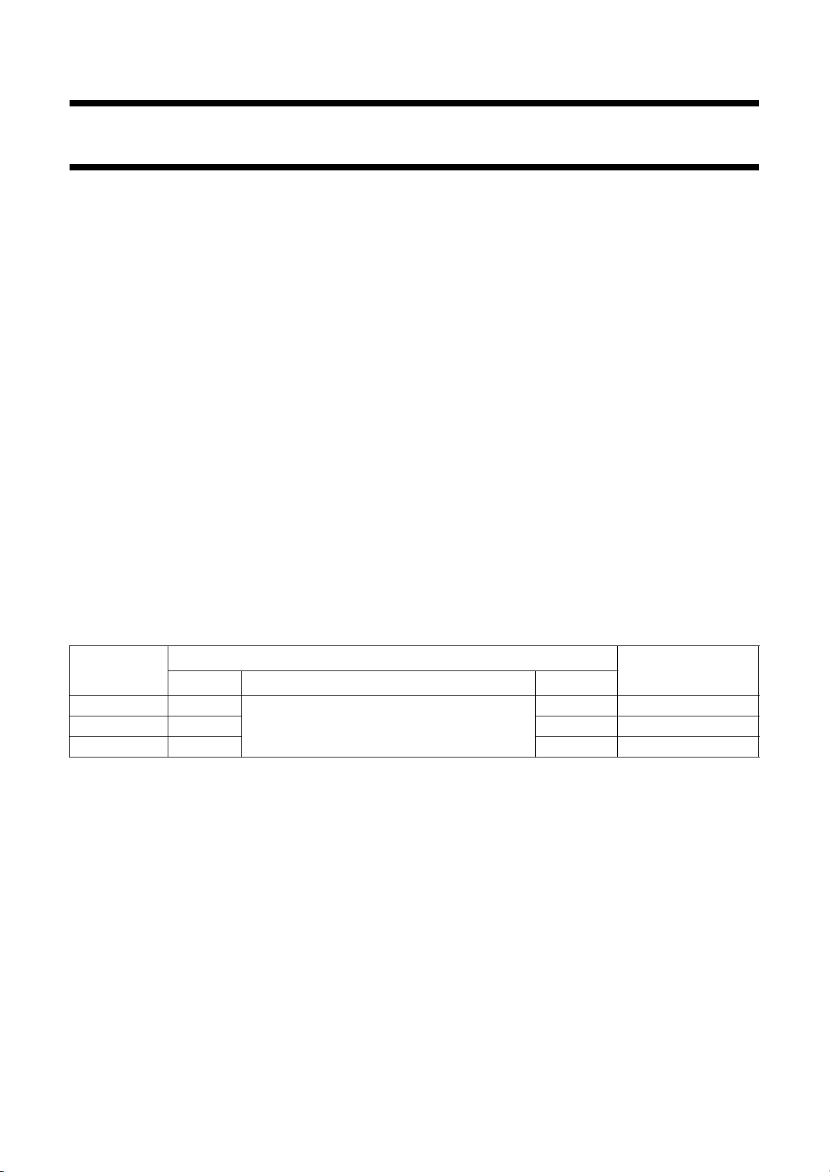
TYPE
NUMBER
TDA8763M/3 SSOP28
TDA8763M/4 SSOP28 SOT341-1 40
TDA8763M/5 SSOP28 SOT341-1 50
NAME DESCRIPTION VERSION
plastic shrink small outline package; 28 leads;
body width 5.3 mm
PACKAGE
SAMPLING
FREQUENCY (MHz)
SOT341-1 30
1996 Feb 13 2
Page 3
Philips Semiconductors Preliminary specification
10-bit high-speed low-power ADC with
TDA8763
internal reference regulator
QUICK REFERENCE DATA
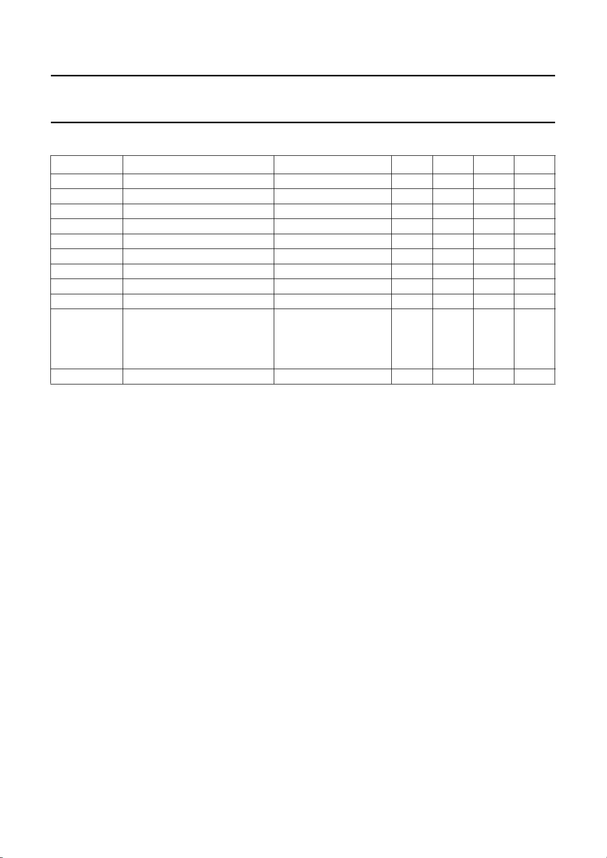
SYMBOL PARAMETER CONDITIONS MIN. TYP. MAX. UNIT
V
CCA
V
CCD
V
CCO
I
CCA
I
CCD
I
CCO
INL integral non-linearity f
DNL differential non-linearity f
AINL AC integral non-linearity note 1 −±1.0 ±2.0 LSB
f
clk(max)
P
tot
analog supply voltage 4.75 5.0 5.25 V
digital supply voltage 4.75 5.0 5.25 V
output stages supply voltage 3.0 3.3 5.25 V
analog supply current − 27 tbf mA
digital supply current − 14 tbf mA
output stages supply current f
= 40 MHz; ramp input − 4 tbf mA
clk
= 40 MHz; ramp input −±0.8 tbf LSB
clk
= 40 MHz; ramp input −±0.5 ±0.9 LSB
clk
maximum clock frequency
TDA8763M/3 30 −−MHz
TDA8763M/4 40 −−MHz
TDA8763M/5 50 −−MHz
total power dissipation f
= 40 MHz; ramp input − 220 tbf mW
clk
Note
1. Full-scale sine wave (f
= 4.43 MHz; f
i
= 40 MHz).
clk
1996 Feb 13 3
Page 4
Philips Semiconductors Preliminary specification
10-bit high-speed low-power ADC with
internal reference regulator
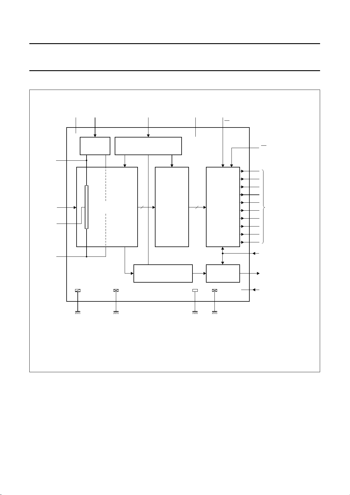
BLOCK DIAGRAM
ook, full pagewidth
analog
voltage input
V
CCA
35
REFERENCE
VOLTAGE
9
8
7
6
REGULATOR
R
LAD
ANALOG -TO - DIGITAL
CONVERTER
V
RT
V
I
V
RM
V
RB
CLKDEC
1
CLOCK DRIVER
LATCHES
V
CCD2
11
TDA8763
OE
10
CMOS
OUTPUTS
2
25
D9
D8
24
D7
23
D6
22
D5
21
20 D4
19
D3
18
D2
17 D1
16 D0
V
13
TDA8763
TC
MSB
data outputs
LSB
CCO
IN RANGE LATCH
4
AGND
analog ground digital ground digital ground
12
DGND2
output ground
CMOS OUTPUT
14
OGND
27
DGND1
Fig.1 Block diagram.
26
28
MBE553
V
CCD1
IR
output
1996 Feb 13 4
Page 5
Philips Semiconductors Preliminary specification
10-bit high-speed low-power ADC with
internal reference regulator
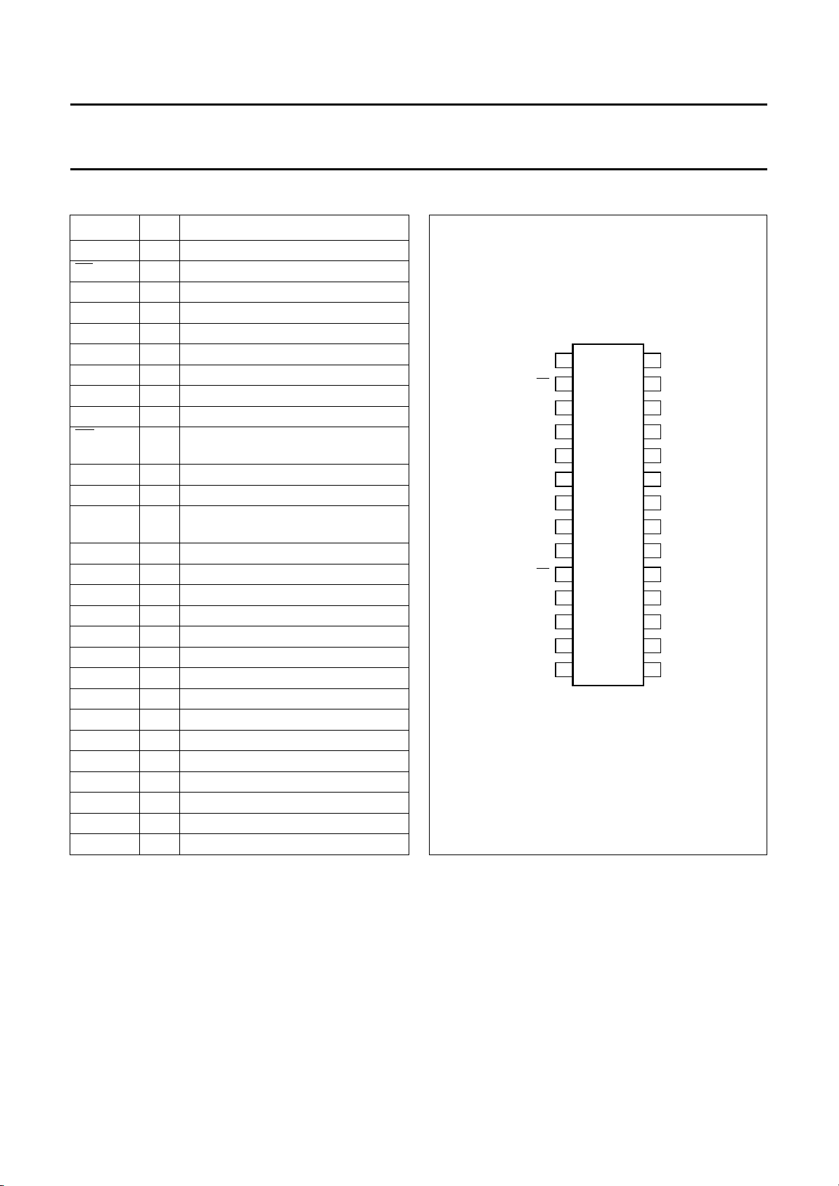
PINNING
SYMBOL PIN DESCRIPTION
CLK 1 clock input
TC 2 two’s complement input (active LOW)
V
CCA
AGND 4 analog ground
DEC 5 decoupling input
V
RB
V
RM
V
I
V
RT
OE 10 output enable input (CMOS level
V
CCD2
DGND2 12 digital ground 2
V
CCO
OGND 14 output ground
n.c. 15 not connected
D0 16 data output; bit 0 (LSB)
D1 17 data output; bit 1
D2 18 data output; bit 2
D3 19 data output; bit 3
D4 20 data output; bit 4
D5 21 data output; bit 5
D6 22 data output; bit 6
D7 23 data output; bit 7
D8 24 data output; bit 8
D9 25 data output; bit 9 (MSB)
IR 26 in range data output
DGND1 27 digital ground 1
V
CCD1
3 analog supply voltage (+5 V)
6 reference voltage BOTTOM input
7 reference voltage MIDDLE
8 analog input voltage
9 reference voltage TOP input
input, active LOW)
11 digital supply voltage 2 (+5 V)
13 supply voltage for output stages
(+3 to 5 V)
28 digital supply voltage 1 (+5 V)
handbook, halfpage
1
CLK
2
TC
V
3
CCA
4
AGND
5
DEC
V
6
RB
V
7
RM
V
RT
OE
V
CCD2
DGND2
V
CCO
OGND
V
I
8
9
10
11
12
13
TDA8763
MBE552
Fig.2 Pin configuration.
TDA8763
V
28
CCD1
27
DGND1
IR
26
25
D9
24
D8
23
D7
22
D6
D5
21
20
D4
D3
19
18
D2
17
D1
16
D0
1514
n.c.
1996 Feb 13 5
Page 6
Philips Semiconductors Preliminary specification
10-bit high-speed low-power ADC with
TDA8763
internal reference regulator
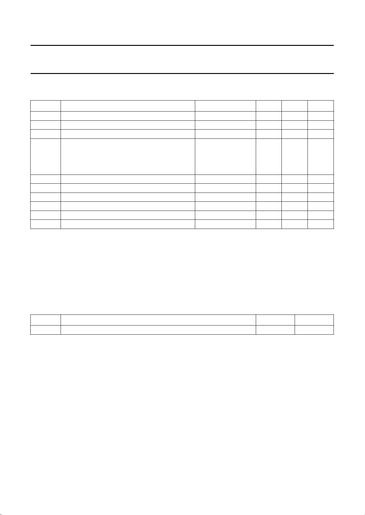
LIMITING VALUES
In accordance with the Absolute Maximum Rating System (IEC 134).
SYMBOL PARAMETER CONDITIONS MIN. MAX. UNIT
V
CCA
V
CCD
V
CCO
∆V
V
I
V
clk(p-p)
I
O
T
stg
T
amb
T
j
CC
analog supply voltage note 1 −0.3 +7.0 V
digital supply voltage note 1 −0.3 +7.0 V
output stages supply voltage note 1 −0.3 +7.0 V
supply voltage difference
V
V
V
CCA
CCA
CCD
− V
− V
− V
CCD
CCO
DDO
−1.0 +1.0 V
−1.0 +4.0 V
−1.0 +4.0 V
input voltage referenced to AGND −0.3 +7.0 V
AC input voltage for switching (peak-to-peak value) referenced to DGND − V
CCD
V
output current − 10 mA
storage temperature −55 +150 °C
operating ambient temperature −40 +85 °C
junction temperature − +150 °C
Note
1. The supply voltages V
CCA
, V
CCD
and V
may have any value between −0.3 V and +7.0 V provided that the supply
CCO
voltage differences ∆VCC are respected.
HANDLING
Inputs and outputs are protected against electrostatic discharges in normal handling. However, to be totally safe, it is
desirable to take normal precautions appropriate to handling integrated circuits.
THERMAL CHARACTERISTICS
SYMBOL PARAMETER VALUE UNIT
R
th j-a
thermal resistance from junction to ambient in free air 110 K/W
1996 Feb 13 6
Page 7
Philips Semiconductors Preliminary specification
10-bit high-speed low-power ADC with
TDA8763
internal reference regulator
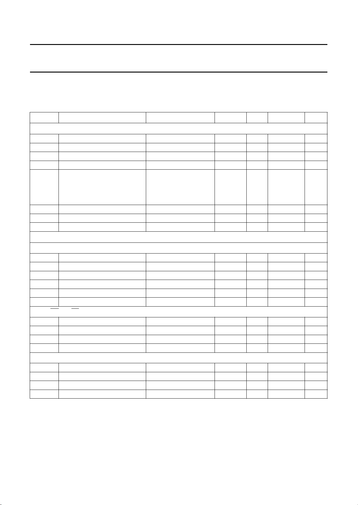
CHARACTERISTICS
V
CCA=V3
AGND and DGND shorted together; T
V
CCO
SYMBOL PARAMETER CONDITIONS MIN. TYP. MAX. UNIT
Supply
V
CCA
V
CCD1
V
CCD2
V
CCO
∆V
I
CCA
I
CCD
I
CCO
Inputs
to V4= 4.75 to 5.25 V; V
= 3.3 V; V
i(p-p)
analog supply voltage 4.75 5.0 5.25 V
digital supply voltage 1 4.75 5.0 5.25 V
digital supply voltage 2 4.75 5.0 5.25 V
output stages supply voltage 3.0 3.3 5.25 V
CC
supply voltage difference
V
CCA
V
CCA
V
CCD
analog supply current − 27 tbf mA
digital supply current − 14 tbf mA
output stages supply current f
CCD=V11
=0to+70°C; typical values measured at V
amb
= 2.0 V; CL= 15 pF and T
− V
CCD
− V
CCO
− V
CCO
to V12and V28to V27= 4.75 to 5.25 V; V
=25°C; unless otherwise specified.
amb
CCO=V13
CCA=VCCD
to V14= 3.0 to 5.25 V;
= 5 V and
−0.20 − +0.20 V
−0.20 − +2.25 V
−0.20 − +2.25 V
= 40 MHz; ramp input − 4 tbf mA
clk
LOCK INPUT CLK (REFERENCED TO DGND); note 1
C
V
IL
V
IH
I
IL
I
IH
Z
i
C
i
LOW level input voltage 0 − 0.3V
HIGH level input voltage 0.7V
LOW level input current V
HIGH level input current V
input impedance f
input capacitance f
= 0.3V
clk
= 0.7V
clk
=40MHz − 2 − kΩ
clk
=40MHz − 2 − pF
clk
INPUTS OE AND TC (REFERENCED TO DGND); see Table 2
V
IL
V
IH
I
IL
I
IH
V
(ANALOG INPUT VOLTAGE REFERENCED TO AGND)
I
I
IL
I
IH
Z
i
C
i
LOW level input voltage 0 − 0.3V
HIGH level input voltage 0.7V
LOW level input current VIL= 0.3V
HIGH level input current VIH= 0.7V
LOW level input current VI=VRB= 1.3 V − 0 −µA
HIGH level input current VI=VRT= 3.67 V − 35 −µA
input impedance fi= 4.43 MHz − 8 − kΩ
input capacitance fi= 4.43 MHz − 5 − pF
CCD
CCD
CCD
CCD
V
V
CCD
− V
CCD
CCD
−10+1 µA
− 210 µA
V
V
CCD
− V
CCD
CCD
−1 −− µA
−−1 µA
1996 Feb 13 7
Page 8
Philips Semiconductors Preliminary specification
10-bit high-speed low-power ADC with
TDA8763
internal reference regulator
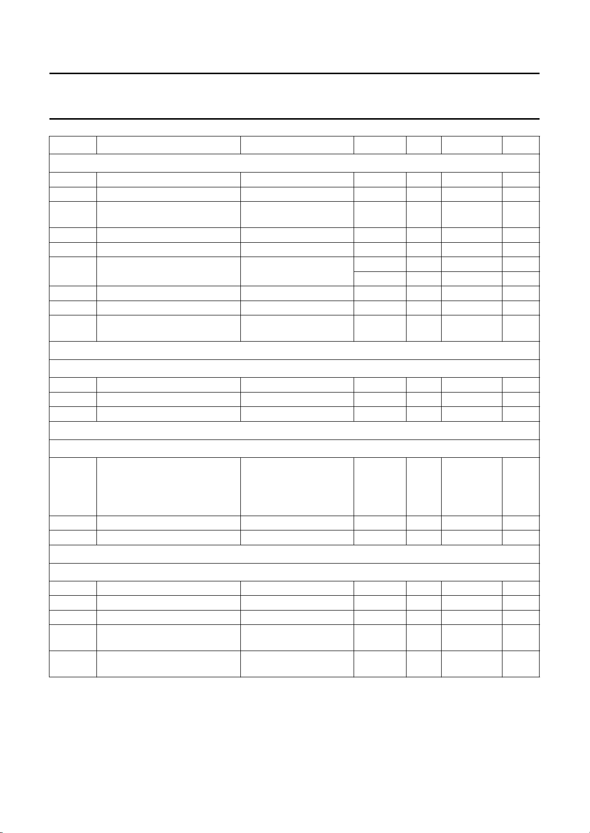
SYMBOL PARAMETER CONDITIONS MIN. TYP. MAX. UNIT
Reference voltages for the resistor ladder using the internal voltage regulator; see Table 1
V
RB
V
RT
V
diff
I
ref
R
LAD
TC
RLAD
V
osB
V
osT
V
i(p-p)
Outputs
IGITAL OUTPUTS D9 TO D0 AND IR (REFERENCED TO OGND)
D
V
OL
V
OH
I
OZ
Switching characteristics
reference voltage BOTTOM tbf 1.3 tbf V
reference voltage TOP tbf 3.67 tbf V
differential reference voltage
VRT− V
RB
tbf 2.37 tbf V
reference current VRT− VRB= 2.37 V − 9.7 − mA
resistor ladder − 245 −Ω
temperature coefficient of the
resistor ladder
− 1860 − ppm
− 456 − mΩ/K
offset voltage BOTTOM note2 − 175 − mV
offset voltage TOP note 2 − 175 − mV
analog input voltage
note 3 tbf 2.02 tbf V
(peak-to-peak value)
LOW level output voltage IOL= 1 mA 0 − 0.5 V
HIGH level output voltage IOH= −1mA V
output current in 3-state mode 0.5 V < VO<V
CCO
−0.5 − V
CCO
CCO
V
−20 − +20 µA
LOCK INPUT CLK; see Fig.4; note 1
C
f
clk(max)
maximum clock frequency
TDA8763M/3 30 −− MHz
TDA8763M/4 40 −− MHz
TDA8763M/5 50 −− MHz
t
CPH
t
CPL
clock pulse width HIGH 8 −− ns
clock pulse width LOW 8 −− ns
Analog signal processing
INEARITY
L
INL integral non-linearity f
DNL differential non-linearity f
= 40 MHz; ramp input −±0.8 tbf LSB
clk
= 40 MHz; ramp input −±0.5 ±0.9 LSB
clk
AINL AC integral non-linearity note 4 −±1.0 ±2.0 LSB
OFER offset error middle code;
= 1.3 V; VRT= 3.67 V
V
RB
GER gain error (from device to device)
using internal reference voltage
V
= 1.3 V;
RB
VRT= 3.67 V; note 5
−±1− LSB
− tbf − %
1996 Feb 13 8
Page 9
Philips Semiconductors Preliminary specification
10-bit high-speed low-power ADC with
TDA8763
internal reference regulator
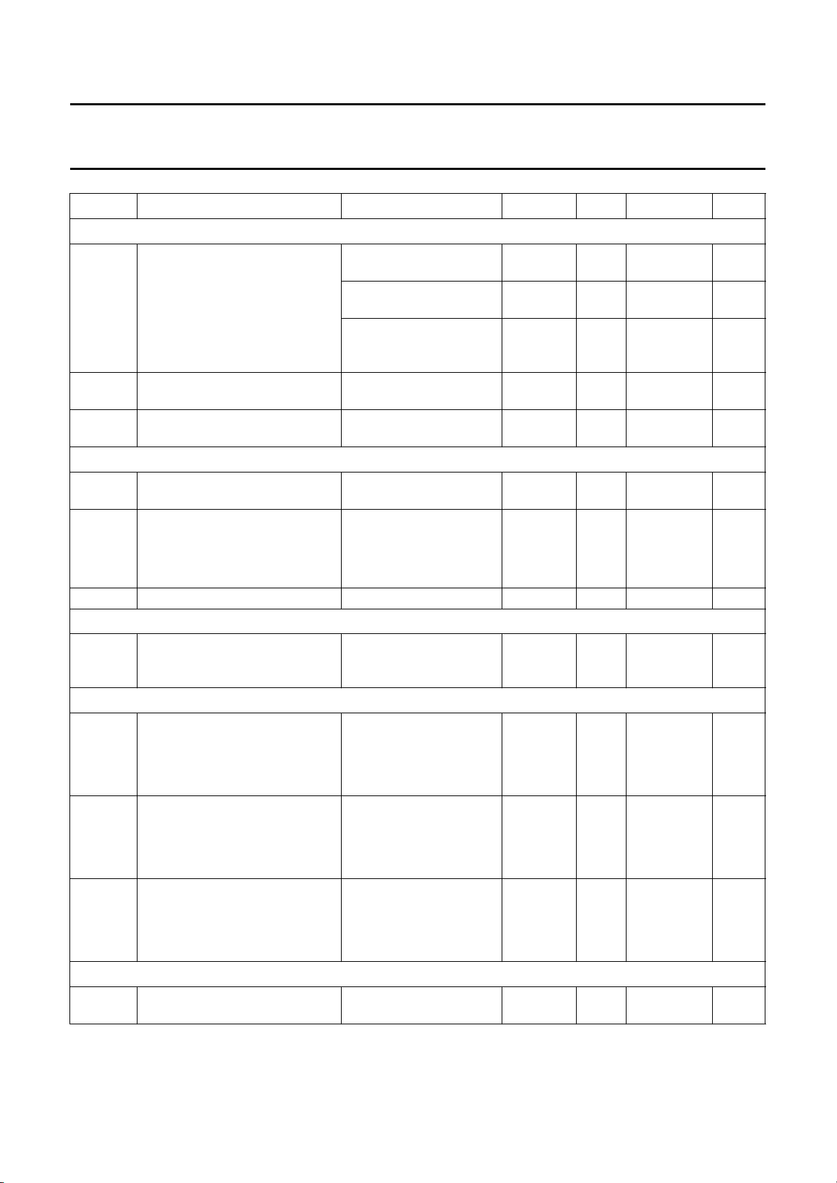
SYMBOL PARAMETER CONDITIONS MIN. TYP. MAX. UNIT
BANDWIDTH (f
B analog bandwidth full-scale sine wave;
t
STLH
t
STHL
HARMONICS (f
h
1
h
all
THD total harmonic distortion f
SIGNAL-TO-NOISE RATIO; see Figs 7 and 8; note 8
S/N signal-to-noise ratio (full scale) without harmonics;
EFFECTIVE BITS; see Figs 7 and 8; note 8
EB effective bits
EB effective bits
EB effective bits
TWO-TONE; note 9
TTIR two-tone intermodulation
= 40 MHz)
clk
− 10 − MHz
note 6
75% full-scale sine wave;
− 14 − MHz
note 6
small signal at mid-scale;
= ±10 LSB at
V
I
− 350 − MHz
code 512; note 6
analog input settling time
LOW-to-HIGH
analog input settling time
HIGH-to-LOW
=40MHZ); see Figs 7 and 8
clk
fundamental harmonics
full-scale square wave;
− 2.0 tbf ns
see Fig.6; note 7
full-scale square wave;
− 2.5 tbf ns
see Fig.6; note 7
fi= 4.43 MHz −−0dB
(full scale)
harmonics (full scale);
fi= 4.43 MHz
all components
second harmonics −−73 tbf dB
third harmonics −−70 tbf dB
= 4.43 MHz −−68 − dB
i
56 58 − dB
f
= 40 MHz;
clk
fi= 4.43 MHz
TDA8763M/3 f
TDA8763M/4 f
TDA8763M/5 f
=30MHz
clk
= 4.43 MHz − 9.4 − bits
f
i
= 7.5 MHz − 9.1 − bits
f
i
=40MHz
clk
= 4.43 MHz − 9.3 − bits
f
i
= 7.5 MHz − 9.0 − bits
f
i
=50MHz
clk
f
= 4.43 MHz − 9.2 − bits
i
= 7.5 MHz − 8.9 − bits
f
i
f
=40MHz −−68 − dB
clk
rejection
1996 Feb 13 9
Page 10
Philips Semiconductors Preliminary specification
10-bit high-speed low-power ADC with
TDA8763
internal reference regulator
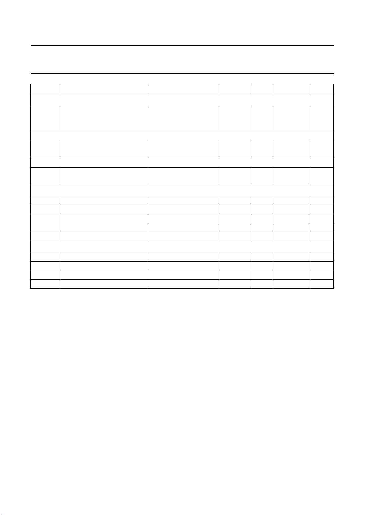
SYMBOL PARAMETER CONDITIONS MIN. TYP. MAX. UNIT
IT ERROR RATE
B
BER bit error rate f
= 50 MHz;
clk
− 10
fi= 4.43 MHz;
VI= ±16 LSB at code 512
DIFFERENTIAL GAIN; note 10
G
diff
differential gain f
= 40 MHz;
clk
− 0.5 − %
PAL modulated ramp
DIFFERENTIAL PHASE; note 10
ϕ
diff
differential phase f
= 40 MHz;
clk
− 0.3 − deg
PAL modulated ramp
Timing (f
t
ds
t
h
t
d
C
L
= 40 MHz; CL= 15 pF); see Fig.4; note 11
clk
sampling delay time −−2ns
output hold time 5 −− ns
output delay time V
= 4.75 V − 13 16 ns
CCO
= 3.15 V − 16 19 ns
V
CCO
digital output load capacitance − 15 40 pF
3-state output delay times; see Fig.5
t
dZH
t
dZL
t
dHZ
t
dLZ
enable HIGH − 14 18 ns
enable LOW − 16 20 ns
disable HIGH − 16 20 ns
disable LOW − 14 18 ns
Notes
1. In addition to a good layout of the digital and analog ground, it is recommended that the rise and fall times of the clock
must not be less than 0.5 ns.
2. Analog input voltages producing code 0 up to and including code 1023:
a) V
b) V
(voltage offset BOTTOM) is the difference between the analog input which produces data equal to 00 and
osB
the reference voltage BOTTOM (VRB) at T
(voltage offset TOP) is the difference between VRT (reference voltage TOP) and the analog input which
osT
produces data outputs equal to code 1023 at T
amb
=25°C.
=25°C.
amb
−13
− times/
sample
1996 Feb 13 10
Page 11
Philips Semiconductors Preliminary specification
10-bit high-speed low-power ADC with
TDA8763
internal reference regulator
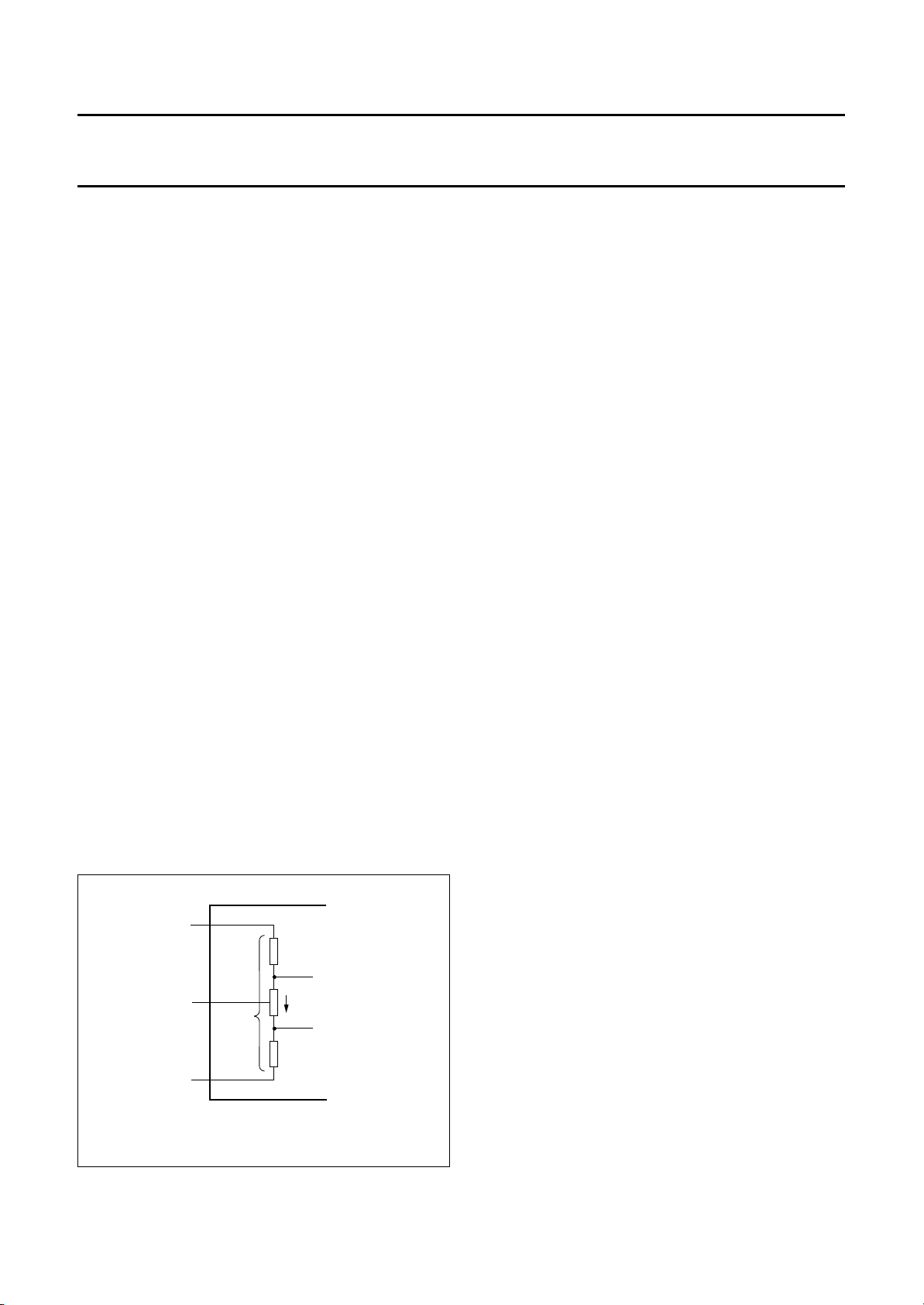
3. In order to ensure the optimum linearity performance of such converter architecture the lower and upper extremities
of the converter reference resistor ladder (corresponding to output codes 0 and 1023 respectively) are connected to
pins V
a) The current flowing into the resistor ladder is and the full-scale input range at the converter,
b) Since R
4. Full-scale sine wave (f
5.
GER
6. The analog bandwidth is defined as the maximum input sine wave frequency which can be applied to the device. No
glitches greater than 2 LSBs, neither any significant attenuation are observed in the reconstructed signal.
7. The analog input settling time is the minimum time required for the input signal to be stabilized after a sharp full-scale
input (square-wave signal) in order to sample the signal and obtain correct output data.
8. Effective bits are obtained via a Fast Fourier Transform (FFT) treatment taking 8K acquisition points per equivalent
fundamental period. The calculation takes into account all harmonics and noise up to half of the clock frequency
(NYQUIST frequency). Conversion to signal-to-noise ratio: S/N = EB × 6.02 + 1.76 dB.
9. Intermodulation measured relative to either tone with analog input frequencies of 4.43 MHz and 4.53 MHz. The two
input signals have the same amplitude and the total amplitude of both signals provides full-scale to the converter.
10. Measurement carried out using video analyser VM700A, where the video analog signal is reconstructed through a
digital-to-analog converter.
11. Output data acquisition: the output data is available after the maximum delay time of t
recommended to have the lowest possible output load and/or to use V
and VRT via offset resistors ROB and ROT as shown in Fig.3.
RB
VRTVRB–
=
I
----------------------------------------- -
L
R
++
OBRLROT
R
== V(
V
to cover code 0 to code 1023, is
, ROB and ROT have similar behaviour with respect to process and temperature variation, the ratio
L
R
----------------------------------------- R
L
++
OBRLROT
will be kept reasonably constant from device to device. Consequently variation of the output
RLIL×
I
----------------------------------------- R
codes at a given input voltage depends mainly on the difference V
L
++
OBRLROT
× VRB)– 0.˙852 V(
RT
− VRB and its variation with temperature and
RT
RTVRB
supply voltage. When several ADCs are connected in parallel and fed with the same reference source, the
matching between each of them is then optimized.
= 4.43 MHz; f
i
–()2V–
V
1023V0
-----------------------------------------------2V
100×=
= 40 MHz).
clk
CCO
at 5 V.
. For 50 MSPS version it is
d
)–×=
handbook, halfpage
V
RT
V
RM
V
RB
Fig.3 Explanation of note 3.
1996 Feb 13 11
9
R
OT
code 1023
R
7
R
LAD
6
L
I
L
R
OB
MGD281
code 0
Page 12
Philips Semiconductors Preliminary specification
10-bit high-speed low-power ADC with
TDA8763
internal reference regulator
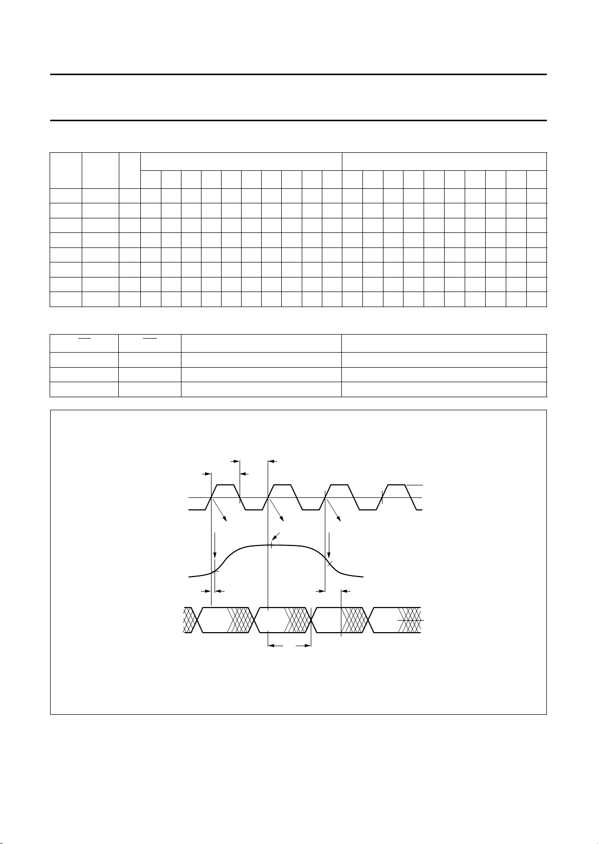
Table 1 Output coding and input voltage (typical values; referenced to AGND, VRB= 1.3 V, VRT= 3.67 V)
STEP V
i(p-p)
IR
D9 D8 D7 D6 D5 D4 D3 D2 D1 D0 D9 D8 D7 D6 D5 D4 D3 D2 D1 D0
U/F <1.475 0 0 0 0 0 0000001000000000
0 1.475 1 0 0 0 0 0000001000000000
1 . 100000000011000000001
. . .....................
. . .....................
1022 . 111111111100111111110
1023 3.495 1 1 1 1 1 1111110111111111
O/F >3.495 0 1 1 1 1 1111110111111111
Table 2 Mode selection
TC OE D9 to D0 IR
X 1 high impedance high impedance
0 0 active; two’s complement active
1 0 active; binary active
BINARY OUTPUT BITS TWO’S COMPLEMENT OUTPUT BITS
handbook, full pagewidth
CLK
V
l
DATA
D0 to D9
t
sample N
DATA
N - 2
CPH
t
t
CPL
sample N + 1
ds
DATA
N - 1
t
d
Fig.4 Timing diagram.
sample N + 2
t
h
DATA
N
DATA
N + 1
MBG916
V
CCO
50%
0 V
V
CCO
50%
0 V
1996 Feb 13 12
Page 13
Philips Semiconductors Preliminary specification
10-bit high-speed low-power ADC with
internal reference regulator
handbook, full pagewidth
V
OE
output
data
output
data
CCD
LOW
t
dLZ
10%
TDA8763
OE
HIGH
t
dZL
50%
15 pF
HIGH
3.3 kΩ
90%
t
dHZ
LOW
S1
V
CCD
50%
t
dZH
50%
TEST
t
dLZ
t
dZL
t
dHZ
t
dZH
S1
V
CCD
V
CCD
DGND
DGND
MBE555 - 1
TDA8763
fOE= 100kHz.
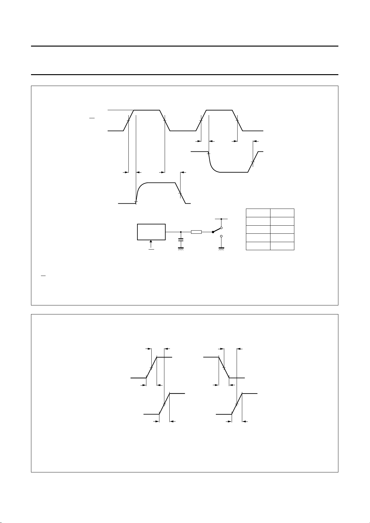
Fig.5 Timing diagram and test conditions of 3-state output delay time.
2 ns
t
STHL
50%
50%
0.5 ns
code 1023
V
code 0
CLK
MBE566
t
STLH
I
50%
2 ns
50%
0.5 ns
1996 Feb 13 13
Fig.6 Analog input settling-time diagram.
Page 14
Philips Semiconductors Preliminary specification
10-bit high-speed low-power ADC with
internal reference regulator
amplitude
(dB)
100
120
0
20
40
60
80
0 2.50 5.00
handbook, full pagewidth
TDA8763
MBG919
12.57.50 10.0 15 17.5 20.0
f (MHz)
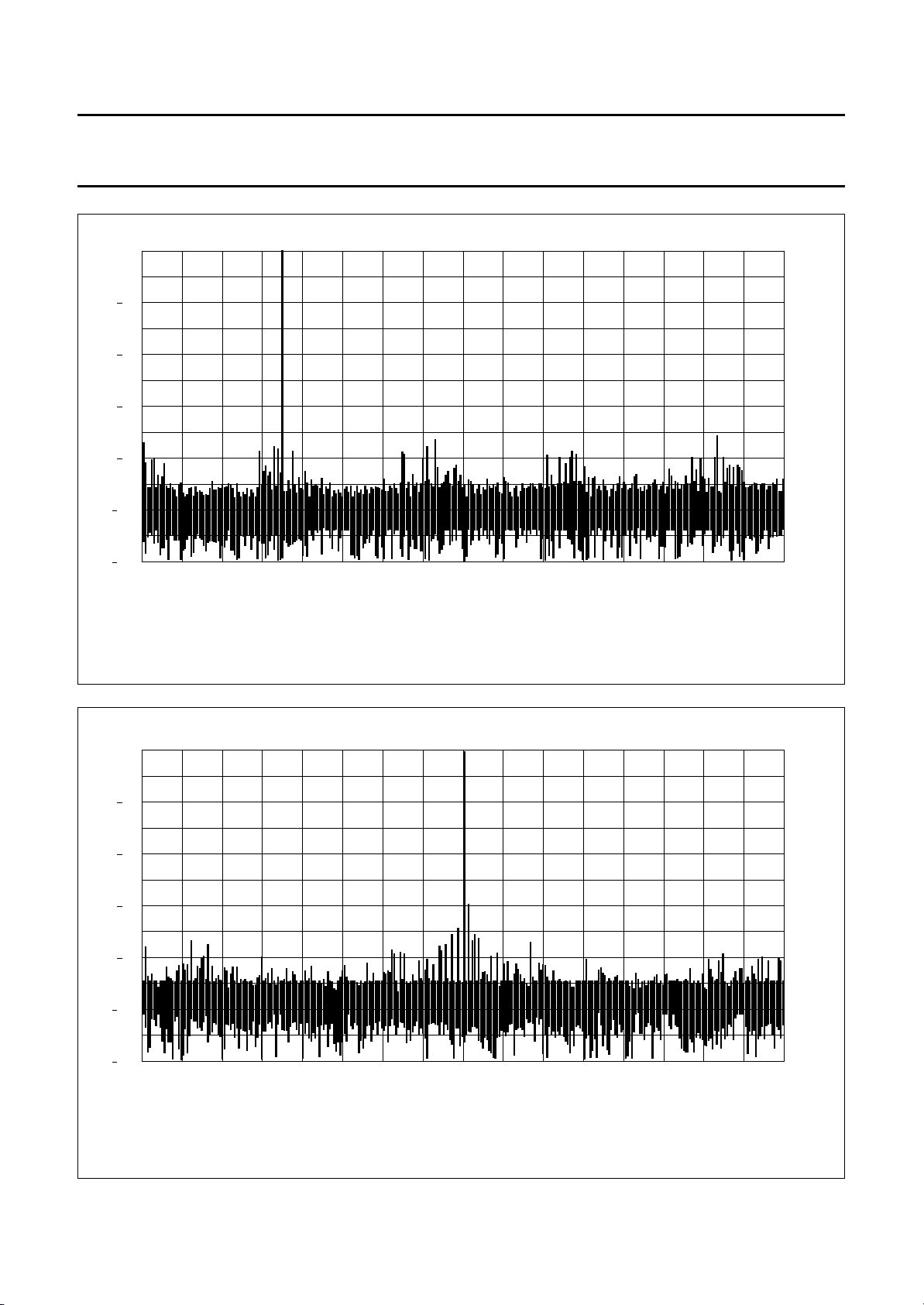
Effective bits: 9.38; THD= −68.52 dB.
Harmonic levels (dB): 2nd = −75.42; 3rd = −76.62; 4th = −79.05; 5th = −72.33; 6th = −77.17.
Fig.7 Typical Fast Fourier Transform (f
amplitude
(dB)
100
120
0
20
40
60
80
0 2.50 5.00
handbook, full pagewidth
= 40 MHz; fi= 4.43 MHz).
clk
12.57.50 10.0 15.0 17.5 20.0
MBG920
f (MHz)
Effective bits: 8.67; THD = −57.38 dB.
Harmonic levels (dB): 2nd = −64.65; 3rd = −58.83; 4th = −76.15; 5th = −68.49; 6th = −78.57.
1996 Feb 13 14
Fig.8 Typical Fast Fourier Transform (f
= 40 MHz; fi= 10 MHz).
clk
Page 15
Philips Semiconductors Preliminary specification
10-bit high-speed low-power ADC with
internal reference regulator
INTERNAL PIN CONFIGURATIONS
handbook, halfpage
MBG915
V
CCO
D9 to D0
IR
OGND
handbook, halfpage
V
CCA
V
I
AGND
TDA8763
MGC040 - 1
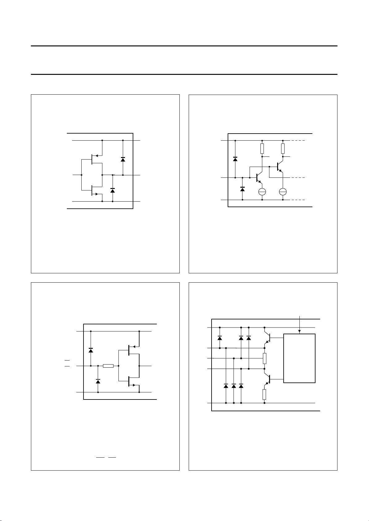
Fig.9 CMOS data and in range outputs.
handbook, halfpage
V
(TC)
OGND
CCO
OE
MBE557
handbook, halfpage
V
CCA
V
RT
V
RM
V
RB
AGND
Fig.10 Analog inputs.
R
LAD
REGULATOR
DEC
MBE558 - 1
Fig.11 OE (TC) input.
1996 Feb 13 15
Fig.12 VRB, VRM and VRT.
Page 16
Philips Semiconductors Preliminary specification
10-bit high-speed low-power ADC with
internal reference regulator
handbook, halfpage
V
CCD
CLK
DGND
1/2V
CCD
MBE559 - 1
TDA8763
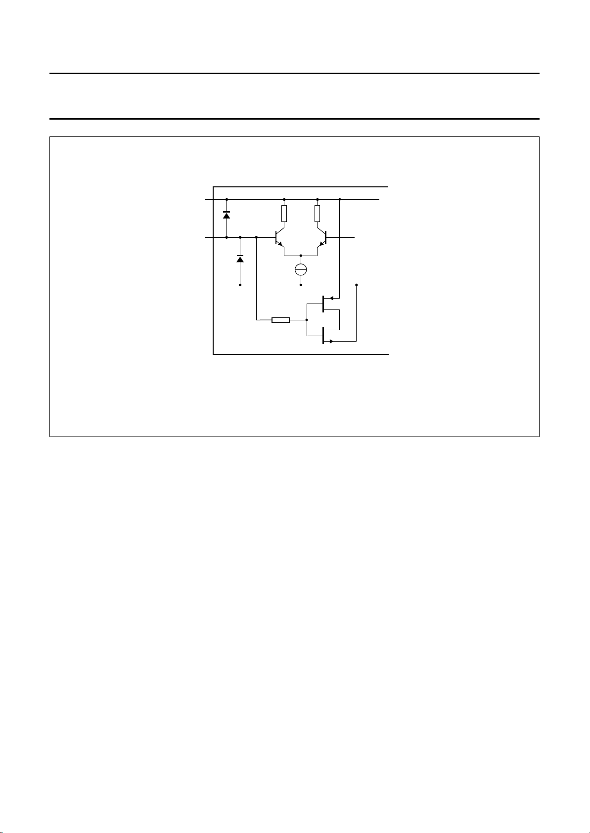
Fig.13 CLK input.
1996 Feb 13 16
Page 17
Philips Semiconductors Preliminary specification
10-bit high-speed low-power ADC with
internal reference regulator
APPLICATION INFORMATION
handbook, halfpage
V
AGND1
1 nF
AGND
100 nF
AGND
100 nF
AGND
100 nF
AGND
V
V
RM
V
V
CCD2
CLK
CCA
DEC
RB
RT
TC
OE
TDA8763
V
1
2
3
4
5
(1)
6
(1)
7
V
(1)
TDA8763
I
8
9
10
11
28
27
26
25
24
23
22
21
20
19
18
CCD1
DGND1
IR
D9
D8
D7
D6
D5
D4
D3
D2
DGND2
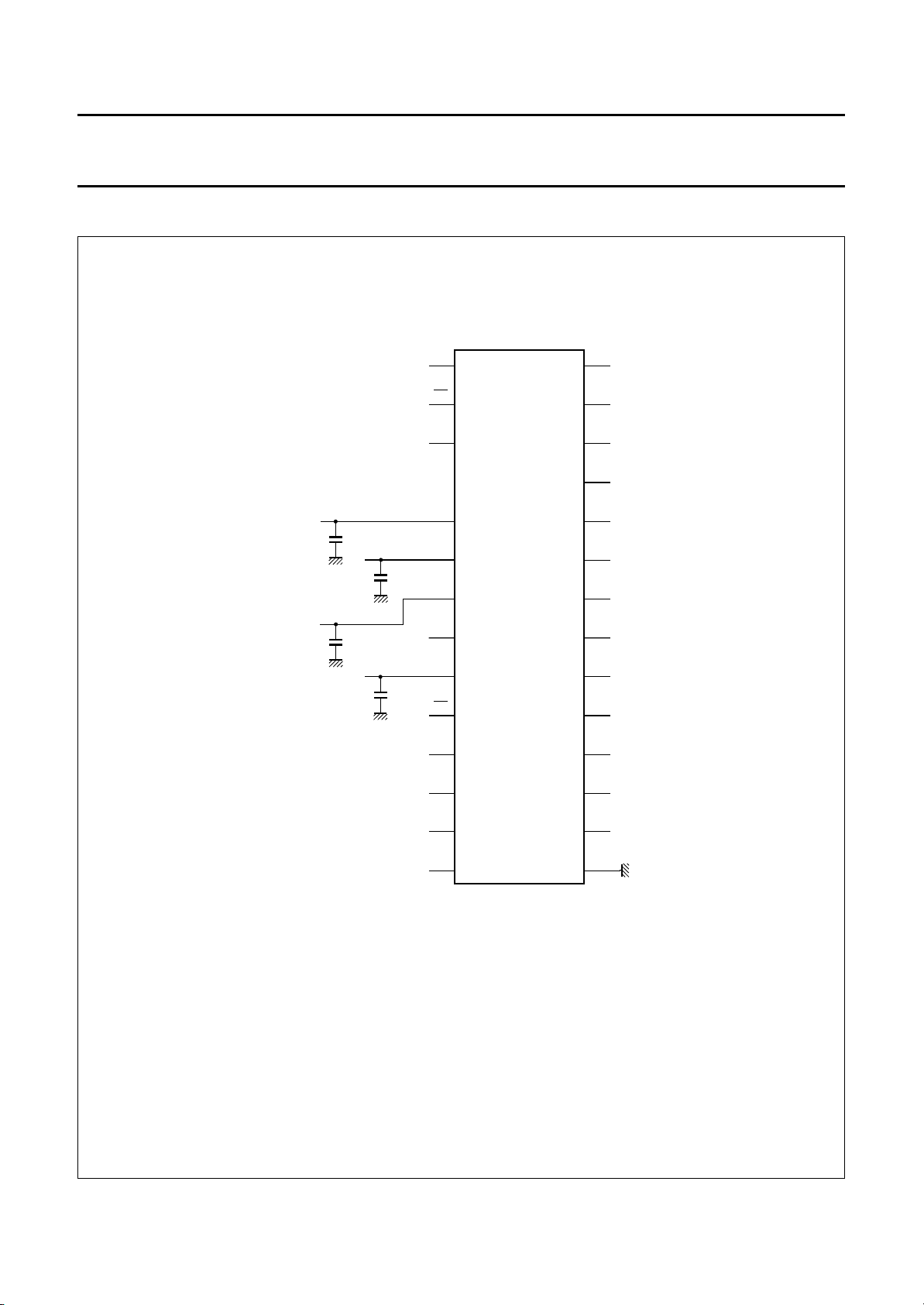
The analog and digital supplies should be separated and decoupled.
The external voltage regulator must be built such that a good supply voltage ripple rejection is achieved with respect to the LSB value. Eventually, the
reference ladder voltages can be derived from a well regulated V
(1) VRB, VRM and VRT are decoupled to AGND.
(2) Pin 15 should be connected to DGND in order to prevent noise influence.
12
V
CCO
13
OGND
14
MBE554 - 1
supply through a resistor bridge and a decoupled capacitor.
CCA
D1
17
D0
16
(2)
n.c.
15
Fig.14 Application diagram.
1996 Feb 13 17
Page 18
Philips Semiconductors Preliminary specification
10-bit high-speed low-power ADC with
internal reference regulator
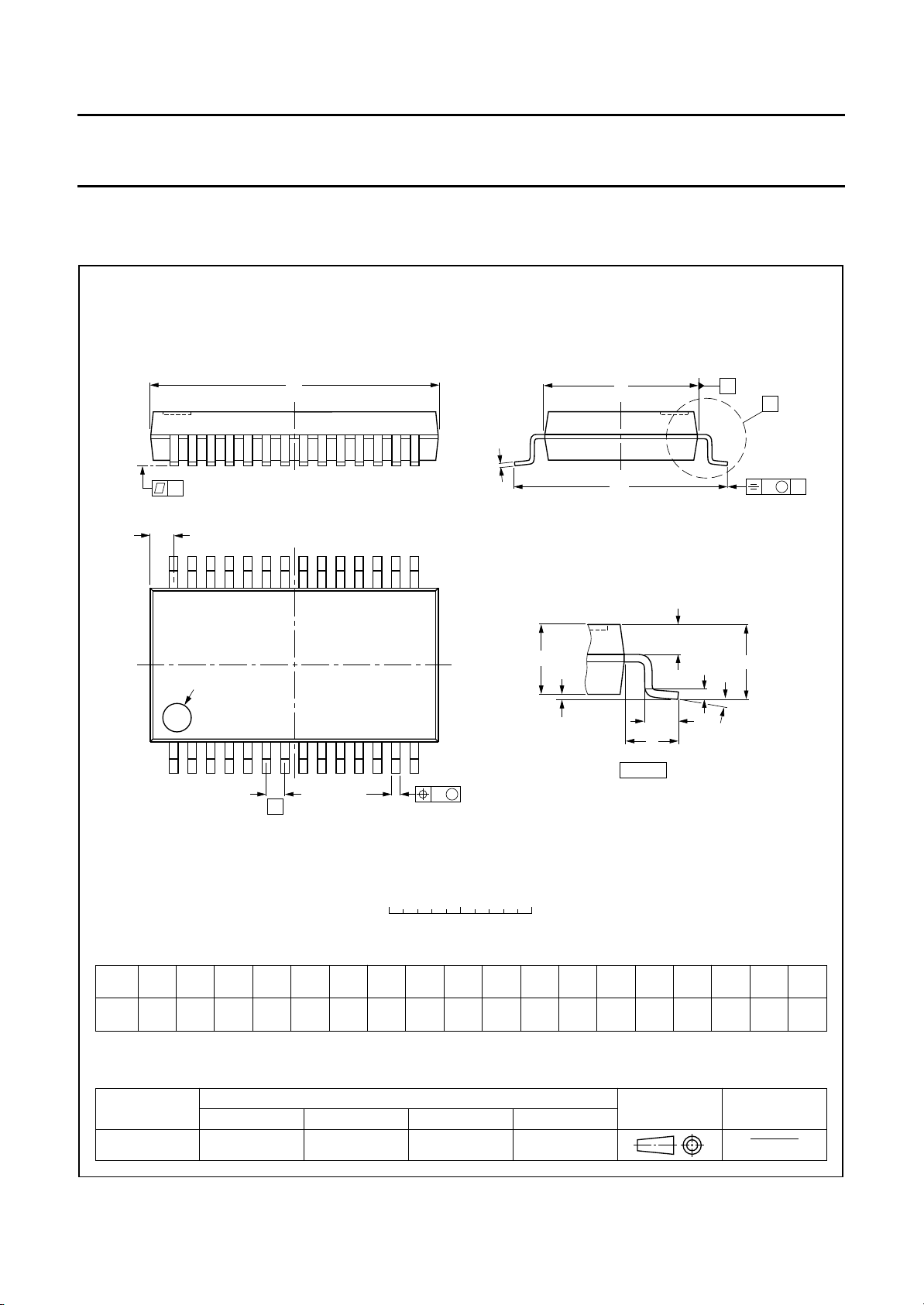
PACKAGE OUTLINE
SSOP28: plastic shrink small outline package; 28 leads; body width 5.3 mm
D
c
y
Z
28 15
TDA8763
SOT341-1
E
H
E
A
X
v M
A
pin 1 index
114
w M
b
e
DIMENSIONS (mm are the original dimensions)
mm
A
max.
2.0
0.21
0.05
1.80
1.65
A
b
0.38
0.25
p
cD
0.20
0.09
2
3
0.25
UNIT A1A
Note
1. Plastic or metal protrusions of 0.20 mm maximum per side are not included.
p
0 2.5 5 mm
scale
(1)E(1) (1)
10.4
10.0
eHELLpQZywv θ
5.4
0.65 1.25
5.2
7.9
7.6
Q
A
2
A
1
detail X
0.9
1.03
0.7
0.63
(A )
L
p
L
0.13 0.10.2
A
3
θ
1.1
0.7
o
8
o
0
OUTLINE
VERSION
SOT341-1 MO-150AH
1996 Feb 13 18
REFERENCES
IEC JEDEC EIAJ
EUROPEAN
PROJECTION
ISSUE DATE
93-09-08
95-02-04
Page 19

Philips Semiconductors Preliminary specification
10-bit high-speed low-power ADC with
internal reference regulator
SOLDERING
Introduction
There is no soldering method that is ideal for all IC
packages. Wave soldering is often preferred when
through-hole and surface mounted components are mixed
on one printed-circuit board. However, wave soldering is
not always suitable for surface mounted ICs, or for
printed-circuits with high population densities. In these
situations reflow soldering is often used.
This text gives a very brief insight to a complex technology.
A more in-depth account of soldering ICs can be found in
our
“IC Package Databook”
Reflow soldering
Reflow soldering techniques are suitable for all SSOP
packages.
Reflow soldering requires solder paste (a suspension of
fine solder particles, flux and binding agent) to be applied
to the printed-circuit board by screen printing, stencilling or
pressure-syringe dispensing before package placement.
Several techniques exist for reflowing; for example,
thermal conduction by heated belt. Dwell times vary
between 50 and 300 seconds depending on heating
method. Typical reflow temperatures range from
215 to 250 °C.
Preheating is necessary to dry the paste and evaporate
the binding agent. Preheating duration: 45 minutes at
45 °C.
Wave soldering
Wave soldering isnot recommended for SSOP packages.
This is because of the likelihood of solder bridging due to
closely-spaced leads and the possibility of incomplete
solder penetration in multi-lead devices.
(order code 9398 652 90011).
TDA8763
If wave soldering cannot be avoided, the following
conditions must be observed:
• A double-wave (a turbulent wave with high upward
pressure followed by a smooth laminar wave)
soldering technique should be used.
• The longitudinal axis of the package footprint must
be parallel to the solder flow and must incorporate
solder thieves at the downstream end.
Even with these conditions, only consider wave
soldering SSOP packages that have a body width of
4.4 mm, that is SSOP16 (SOT369-1) or
SSOP20 (SOT266-1).
During placement and before soldering, the package must
be fixed with a droplet of adhesive. The adhesive can be
applied by screen printing, pin transfer or syringe
dispensing. The package can be soldered after the
adhesive is cured.
Maximum permissible solder temperature is 260 °C, and
maximum duration of package immersion in solder is
10 seconds, if cooled to less than 150 °C within
6 seconds. Typical dwell time is 4 seconds at 250 °C.
A mildly-activated flux will eliminate the need for removal
of corrosive residues in most applications.
Repairing soldered joints
Fix the component by first soldering two diagonallyopposite end leads. Use only a low voltage soldering iron
(less than 24 V) applied to the flat part of the lead. Contact
time must be limited to 10 seconds at up to 300 °C. When
using a dedicated tool, all other leads can be soldered in
one operation within 2 to 5 seconds between
270 and 320 °C.
1996 Feb 13 19
Page 20

Philips Semiconductors Preliminary specification
10-bit high-speed low-power ADC with
TDA8763
internal reference regulator
DEFINITIONS
Data sheet status
Objective specification This data sheet contains target or goal specifications for product development.
Preliminary specification This data sheet contains preliminary data; supplementary data may be published later.
Product specification This data sheet contains final product specifications.
Limiting values
Limiting values given are in accordance with the Absolute Maximum Rating System (IEC 134). Stress above one or
more of the limiting values may cause permanent damage to the device. These are stress ratings only and operation
of the device at these or at any other conditions above those given in the Characteristics sections of the specification
is not implied. Exposure to limiting values for extended periods may affect device reliability.
Application information
Where application information is given, it is advisory and does not form part of the specification.
LIFE SUPPORT APPLICATIONS
These products are not designed for use in life support appliances, devices, or systems where malfunction of these
products can reasonably be expected to result in personal injury. Philips customers using or selling these products for
use in such applications do so at their own risk and agree to fully indemnify Philips for any damages resulting from such
improper use or sale.
1996 Feb 13 20
 Loading...