

Page 1
INTEGRATED CIRCUITS
DATA SH EET
TDA8758
YC 8-bit low-power
analog-to-digital video interface
Product specification
Supersedes data of 1995 Mar 22
File under Integrated Circuits, IC02
1996 Feb 01
Page 2
Philips Semiconductors Product specification
YC 8-bit low-power analog-to-digital
video interface
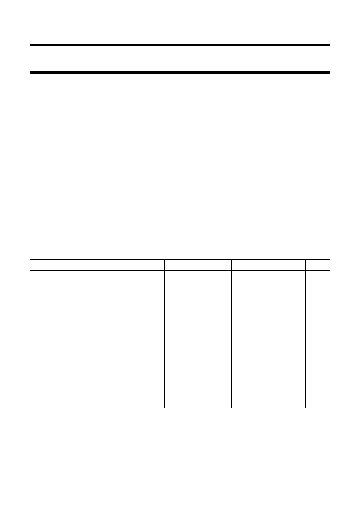
FEATURES
• Two 8-bit ADCs:
– one Luminance or CVBS channel
– one Chrominance channel
• Sampling rate up to 32 MHz
• Binary or two's complement 3-state TTL outputs for
each channel
• Internal reference voltage regulator
• TTL-compatible digital inputs and outputs
• Power dissipation of 530 mW (typical)
• Input selector circuit (five selectable video inputs for
CVBS or YC processing)
• Peak white enable input
• Clamp and Automatic Gain Control (AGC) functions for
Y/CVBS channel (clamping on code 64 and Peak White
level control at code 255)
• Clamp function for C channel (code 128)
• No sample-and-hold circuit required.
TDA8758
APPLICATIONS
• Video signal decoding
• Digital picture processing
• Frame grabbing
• Multimedia with the Philips Desktop Video chip set (and
especially SAA7196 multistandard decoder and scaler).
GENERAL DESCRIPTION
The TDA8758 is an 8-bit video high-speed low-power
analog-to-digital conversion (ADC) interface for YC and
CVBS signal processing. It converts 1-of-3 CVBS input
signals or 1-of-2 YC input signals into binary or two’s
complement words at a sampling rate of 32 MHz.
All analog signal inputs are digitally clamped and an ADC
interface is provided on the Y/CVBS channel. A fast
precharge on clamp and AGC is provided for start-up.
All digital inputs and outputs are TTL compatible.
QUICK REFERENCE DATA
SYMBOL PARAMETER CONDITIONS MIN. TYP. MAX. UNIT
V
V
V
I
CCA
I
CCD
I
CCO
CCA
CCD
CCO
analog supply voltage 4.75 5.0 5.25 V
digital supply voltage 4.75 5.0 5.25 V
output stages supply voltage 4.75 5.0 5.25 V
analog supply current − 59 70 mA
digital supply current − 28 40 mA
output supply current CL=15pF − 19 28 mA
ILE DC integral linearity error −±0.75 ±1.5 LSB
DLE DC differential linearity error −±0.4 ±1.0 LSB
EB effective bits
(from video input to digital outputs)
f
clk(max)
maximum clock frequency 30 32 − MHz
B maximum −3 dB bandwidth
= 32 MHz;
f
clk
fi= 4.43 MHz
full-scale; 0 dB gain − 15 − MHz
− 7.1 − bits
(input preamplifier)
α
ct
crosstalk between Y and C channels
−−63 −55 dB
and each video input
P
tot
total power dissipation − 530 724 mW
ORDERING INFORMATION
TYPE
NUMBER
NAME DESCRIPTION VERSION
TDA8758G LQFP48 plastic low profile quad flat package; 48 leads; body 7 × 7 × 1.4 mm SOT313-2
1996 Feb 01 2
PACKAGE
Page 3
Philips Semiconductors Product specification
YC 8-bit low-power analog-to-digital video
interface
BLOCK DIAGRAM
handbook, full pagewidth
CHROM2
CHROM1
CVBS3
2
4
6
SEL2
5
INPUT
SELECTOR
V
CCD
V
CCA
10 21 41 32
V
V
CCO1
CLAMP
LEVEL 128
CCO2
C
TDA8758
CLPC
V
CCA
REG2
REG1
SDN
ANOUTC
48 45 8 44 17 1 46 15
ADC
COMPARATOR
DEC2
DEC1
TTL
TIMING
GENERATOR
DEC3
TDA8758
8
33
to
40
47
42
C7 to C0
OFC
CLK
Y2/CVBS2
Y1/CVBS1
COMPARATORS
9
11
12 31 43 18 3
SEL1
PWE
AGC &
CLAMP 64
GATE A
GATE B
C
CLPY
713
C
AGC
1614 19 20
ANOUTY
ADC TTL
OGND2
DGND
OGND1
22
23
30
AGND
to
OFY
Y7 to Y0
8
MGB469 - 1
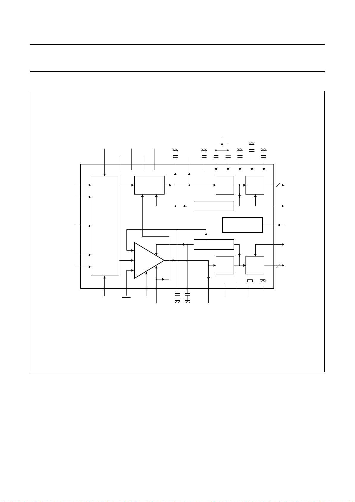
Fig.1 Block diagram.
1996 Feb 01 3
Page 4
Philips Semiconductors Product specification
YC 8-bit low-power analog-to-digital video
interface
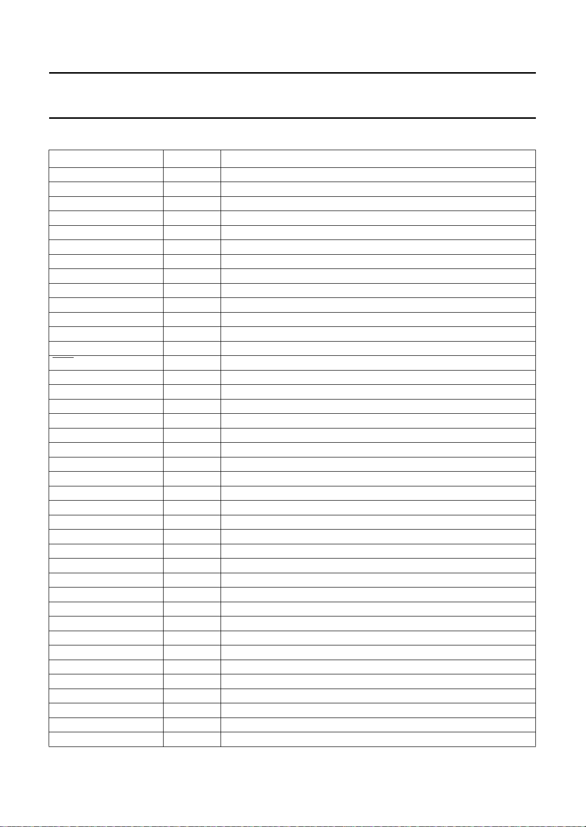
PINNING
SYMBOL PIN DESCRIPTION
DEC1 1 decoupling input 1
CHROM2 2 chrominance analog voltage input 2
AGND 3 analog ground
CHROM1 4 chrominance analog voltage input 1
SEL2 5 selection control input 2
CVBS3 6 luminance analog voltage input 3
C
CLPY
SDN 8 stabilizer decoupling node
Y2/CVBS2 9 luminance analog voltage input 2
V
CCA
Y1/CVBS1 11 luminance analog voltage input 1
SEL1 12 selection control input 1
C
AGC
PWE 14 peak white enable input (active LOW)
DEC3 15 decoupling input 3
ANOUTY 16 analog output for Y channel
REG2 17 decoupling input 2 (internal stabilization loop decoupling)
DGND 18 digital ground
GATE A 19 AGC control input
GATE B 20 clamp control input
V
CCD
OFY 22 Y channel output format/chip enable (3-state input)
Y7 23 Y channel data output; bit 7 (MSB)
Y6 24 Y channel data output; bit 6
Y5 25 Y channel data output; bit 5
Y4 26 Y channel data output; bit 4
Y3 27 Y channel data output; bit 3
Y2 28 Y channel data output; bit 2
Y1 29 Y channel data output; bit 1
Y0 30 Y channel data output; bit 0 (LSB)
OGND2 31 output ground 2
V
CCO2
C7 33 C channel data output; bit 7 (MSB)
C6 34 C channel data output; bit 6
C5 35 C channel data output; bit 5
C4 36 C channel data output; bit 4
C3 37 C channel data output; bit 3
C2 38 C channel data output; bit 2
C1 39 C channel data output; bit 1
C0 40 C channel data output; bit 0 (LSB)
7 Y channel clamping capacitor
10 analog supply voltage (+5 V)
13 AGC capacitor
21 digital supply voltage (+5 V)
32 output supply voltage 2 (+5 V)
TDA8758
1996 Feb 01 4
Page 5
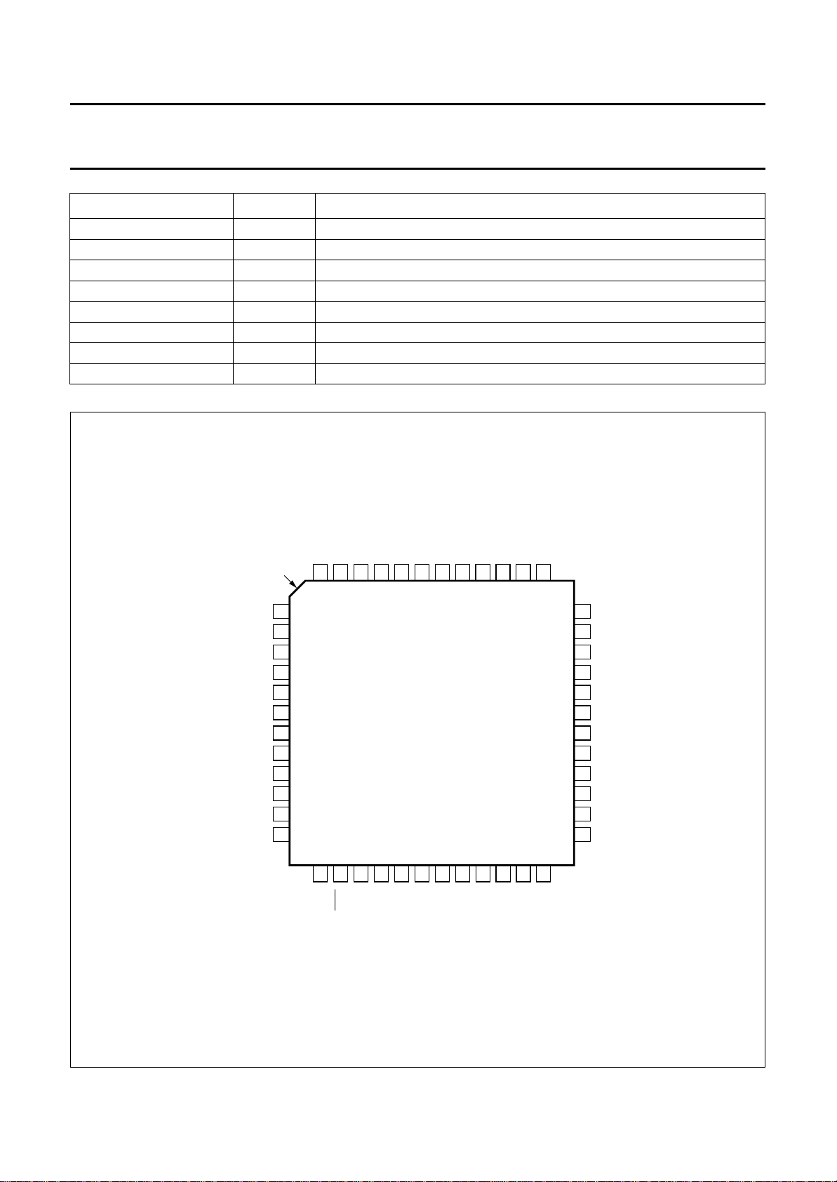
Philips Semiconductors Product specification
YC 8-bit low-power analog-to-digital video
interface
SYMBOL PIN DESCRIPTION
V
CCO1
CLK 42 clock input
OGND1 43 output ground 1
REG1 44 decoupling input 1 (internal stabilization loop decoupling)
ANOUTC 45 analog output for C channel
DEC2 46 decoupling input 2
OFC 47 C channel output format/chip enable (3-state input)
C
CLPC
41 output supply voltage 1 (+5 V)
48 C channel clamping capacitor
TDA8758
handbook, full pagewidth
pin 1
index
corner
DEC1
CHROM2
AGND
CHROM1
SEL2
CVBS3
C
CLPY
SDN
Y2/CVBS2
V
CCA
Y1/CVBS1
SEL1
CLPC
OFC
DEC2
ANOUTC
REG1
45
44
TDA8758
16
17
REG2
ANOUTY
OGND1
DGND
C
48
47
46
1
2
3
4
5
6
7
8
9
10
11
12
13
14
15
AGC
PWE
DEC3
C
43
18
CCO1
CLK
V
42
41
19
20
GATE A
GATE B
C0C1C2
40
39
38
21
22
23
Y7
OFY
CCD
V
C3
24 37
Y6
36
35
34
33
32
31
30
29
28
27
26
25
MGB470
C4
C5
C6
C7
V
CCO2
OGND2
Y0
Y1
Y2
Y3
Y4
Y5
1996 Feb 01 5
Fig.2 Pin configuration.
Page 6

Philips Semiconductors Product specification
YC 8-bit low-power analog-to-digital video
interface
FUNCTIONAL DESCRIPTION
The TDA8758 provides a simple interface between CVBS
or Y/C analog signals and a digital colour decoder.
Video inputs selection
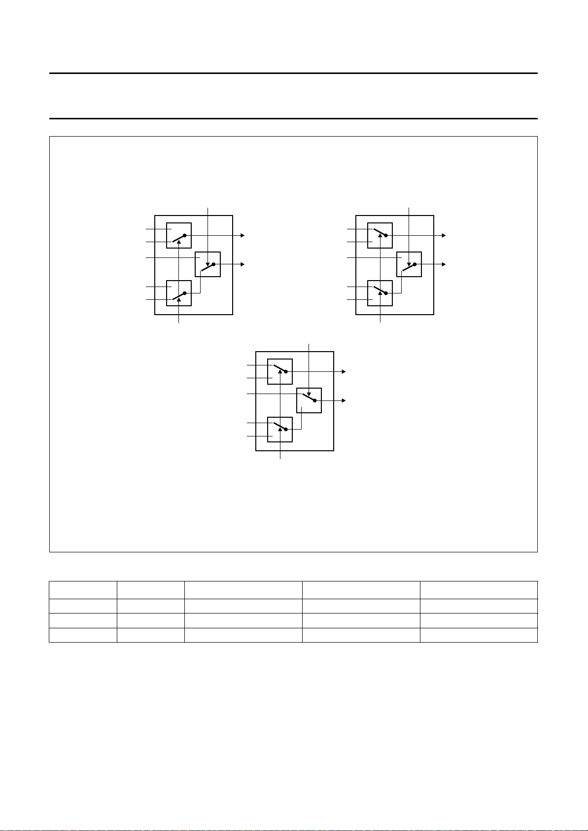
The input selector allows a choice from different video
sources, and has one of the following configurations:
A: Two Y/C and one CVBS signals
B: One Y/C and two CVBS signals
C: Three CVBS signals (only the Y channel is used).
The wiring of the five video inputs (pins 2, 4, 6, 9 and 11)
and the control of the two selection inputs (pins 5 and 12)
will depend on the available video sources.
• In configuration A, connect as follows:
– Y1 to pin 11
– C1 to pin 4
– Y2 to pin 9
– C2 to pin 2
– CVBS3 to pin 6.
Keep SEL2 (pin 5) LOW and select Y1/C1 or Y2/C2 by
switching SEL1 (pin 12).
CVBS3 is selected with SEL1 and SEL2 HIGH.
• In configuration B, replace Y1 (or Y2) by a CVBS input
(no more C1 or C2). The selection mode is the same.
• In configuration C, connect as follows:
– CVBS1 to pin 11
– CVBS2 to pin 9
– CVBS3 to pin 6.
Use both SEL1 and SEL2 to select inputs.
TDA8758
Synchronization pulses
GATE A and GATE B pulses are synchronization pulses
occurring during the sync period and rear porch
respectively. They should be distinct.
On the Y channel, the digital output of the ADC is
compared to internal digital reference levels. The resultant
outputs control the charge or discharge current of a
capacitor connected to the C
this capacitor controls the gain of the video amplifier.
This is the control loop.
The sync level comparator is active during a positive-going
pulse at the GATE A input. This means that sync pulse of
the composite video signal is used as an amplitude
reference. The bottom of the sync pulse is adjusted to
obtain a digital output of logic 1 at the converter Y output.
As the black level is digital level 64, the sync pulse will
have a digital amplitude of 64 LSBs.
The Peak White control loop is active when the selection
PWE is LOW. Then, if the Y video signal exceeds the
pin
digital code of 255, it will be limited to avoid any over-range
of the converter.
The clamp level control is accomplished by using the same
techniques as used for the gain control. On both Y and C
channels, the black level digital comparators are active
during a positive-going pulse at the GATE B input. On the
Y channel, the clamping capacitor connected to the C
pin will be charged or discharged to adjust the digital
output to code 64. On the C channel, the clamping
capacitor connected to the C
discharged to adjust the digital output to code 128.
pin. The voltage across
AGC
pin will be charged or
CLPC
CLPY
Remark: the video inputs selection is a static selection.
1996 Feb 01 6
Page 7
Philips Semiconductors Product specification
YC 8-bit low-power analog-to-digital video
TDA8758
interface
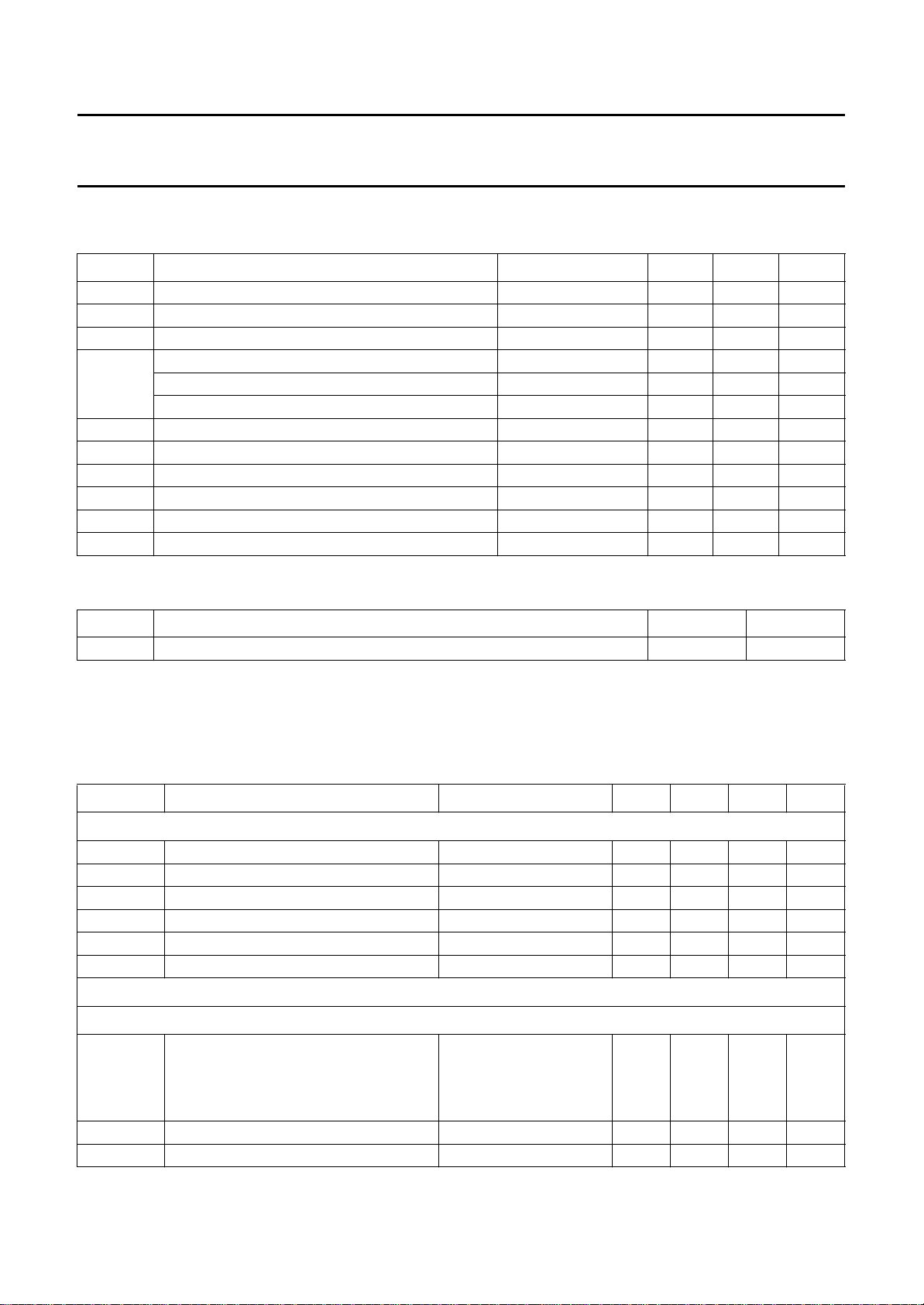
LIMITING VALUES
In accordance with the Absolute Maximum Rating System (IEC 134).
SYMBOL PARAMETER CONDITIONS MIN. MAX. UNIT
V
CCA
V
CCD
V
CCO
∆V
V
I
V
clk(p-p)
I
O
T
stg
T
amb
T
j
CC
analog supply voltage −0.3 +7.0 V
digital supply voltage −0.3 +7.0 V
output supply voltage −0.3 +7.0 V
supply voltage difference between V
supply voltage difference between V
supply voltage difference between V
CCA
CCO
CCA
and V
and V
and V
CCD
CCD
CCO
−1.0 +1.0 V
−1.0 +1.0 V
−1.0 +1.0 V
input voltage referenced to AGND − 5.0 V
AC input voltage for switching (peak-to-peak value) referenced to DGND − V
CCO
V
output current − +6 mA
storage temperature −55 +150 °C
operating ambient temperature 0 +70 °C
junction temperature − +150 °C
THERMAL CHARACTERISTICS
SYMBOL PARAMETER VALUE UNIT
R
th j-a
thermal resistance from junction to ambient in free air 72 K/W
CHARACTERISTICS
V
CCA=V10
V
CC02=V32
V
CCO
at V
CCA=VCCD=VCCO
to V3= 4.75 to 5.25 V; V
to V31= 4.75 to 5.25 V; AGND and DGND shorted together; V
to V
CCD
= −0.25 to +0.25 V; V
= 5 V and T
CCD=V21
to V
CCA
=25°C; unless otherwise specified.
amb
to V18= 4.75 to 5.25 V; V
= −0.25 to +0.25 V; T
CCO
CCO1=V41
CCA
= 0 to +70 °C; typical values measured
amb
to V43= 4.75 to 5.25 V;
to V
= −0.25 to +0.25 V;
CCD
SYMBOL PARAMETER CONDITIONS MIN. TYP. MAX. UNIT
Supplies
V
CCA
V
CCD
V
CCO
I
CCA
I
CCD
I
CCOtot
analog supply voltage 4.75 5.0 5.25 V
digital supply voltage 4.75 5.0 5.25 V
output stages supply voltage 4.75 5.0 5.25 V
analog supply current − 59 70 mA
digital supply current − 28 40 mA
total output supply current CL=15pF − 19 28 mA
Video amplifier inputs
Y1/CVBS1, Y2/CVBS2, CVBS3, CHROM1
V
I(p-p)
input voltage (peak-to-peak value) AGC load with external
AND CHROM2 INPUTS
capacitor; note 1
Y channel 0.7 − 1.4 V
C channel − 1.0 − V
| input impedance fi= 6 MHz − 25 − kΩ
|Z
i
C
I
input capacitance fi= 6 MHz − 2 − pF
1996 Feb 01 7
Page 8
Philips Semiconductors Product specification
YC 8-bit low-power analog-to-digital video
TDA8758
interface
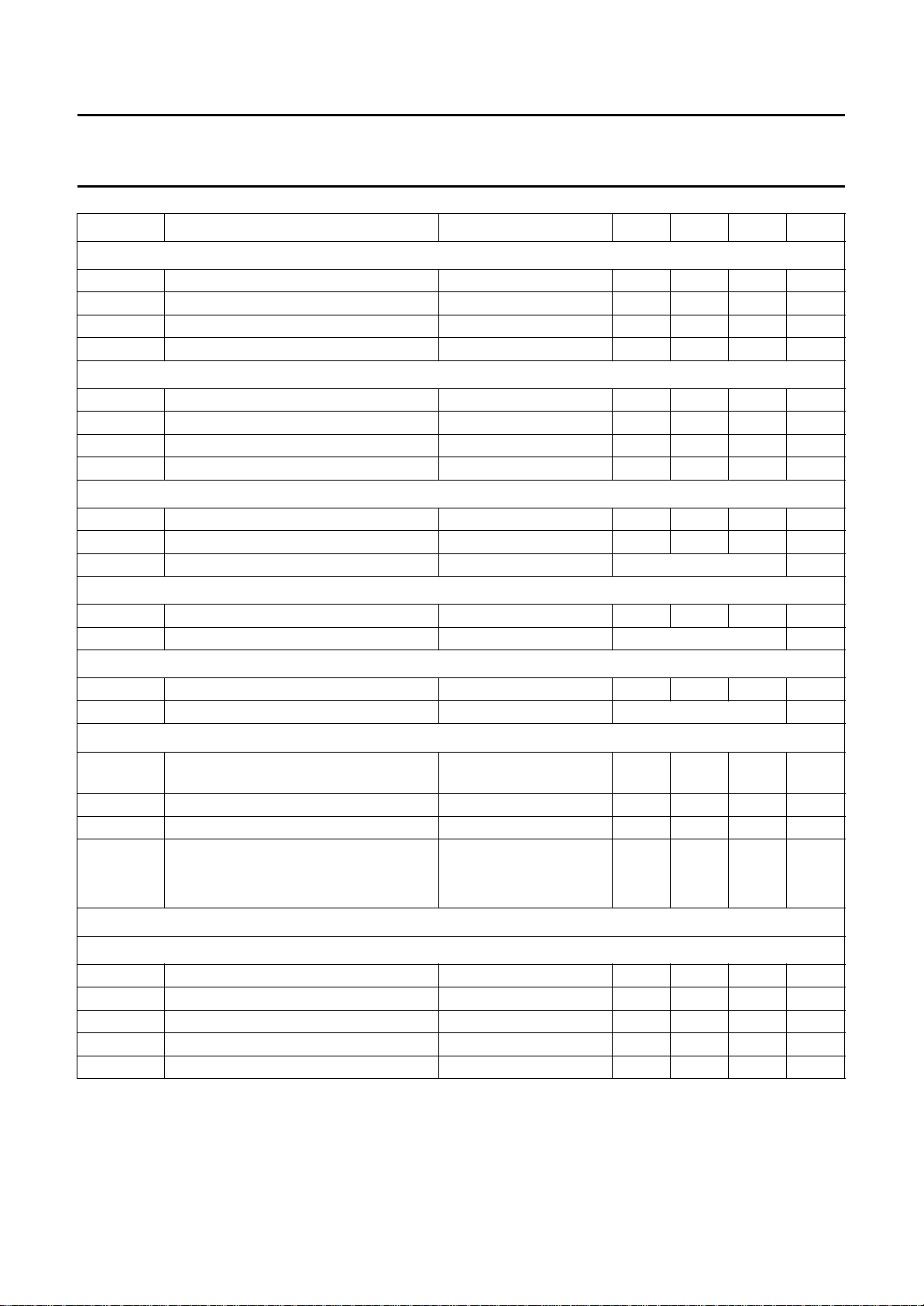
SYMBOL PARAMETER CONDITIONS MIN. TYP. MAX. UNIT
SEL1 AND SEL2 TTL INPUTS; see Table 1
V
IL
V
IH
I
IL
I
IH
GATE A AND GATE B TTL INPUTS; see Figs 5 and 6
V
IL
V
IH
I
IL
I
IH
AGC INPUT (PIN 13); see Fig.8
V
13(min)
V
13(max)
I
12
C-CHANNEL CLAMP INPUT (PIN 48)
V
48
I
48
Y-CHANNEL CLAMP INPUT (PIN 7)
V
7
I
7
Video amplifier dynamic characteristics
α
ct
B −3 dB bandwidth − 15 − MHz
∆G gain range −3 − +3 dB
G
stab
LOW level input voltage 0 − 0.8 V
HIGH level input voltage 2.0 − V
CCD
V
LOW level input current VI= 0.4 V −400 −−µA
HIGH level input current VI= 2.7 V −−20 µA
LOW level input voltage 0 − 0.8 V
HIGH level input voltage 2.0 − V
CCD
V
LOW level input current VI = 0.4 V −400 −−µA
HIGH level input current VI = 2.7 V −−20 µA
AGC voltage for minimum gain at −3dB − 3.3 − V
AGC voltage for maximum gain at +3 dB − 3.75 − V
AGC output current see Table 2
CLAMP voltage for code 128 output − 3.45 − V
CLAMP output current see Table 3
CLAMP voltage for code 64 output − 3.70 − V
CLAMP output current see Table 3
crosstalk between video inputs
V
= 4.75 to 5.25 V −−63 −55 dB
CCA
(pins 2, 4, 6, 9 and 11)
gain stability as a function of:
supply voltage f
= 4.43 MHz −−0.5 %
i
supply voltage and temperature −−6%
Analog-to-digital converter inputs
INPUT (PIN 42)
CLK
V
IL
V
IH
I
IL
I
IH
C
I
LOW level input voltage 0 − 0.8 V
HIGH level input voltage 2.0 − V
LOW level input current V
HIGH level input current V
input capacitance f
1996 Feb 01 8
CCD
= 0.4 V −400 −−µA
clk
= 2.7 V −−20 µA
clk
= 32 MHz − 2 − pF
clk
V
Page 9
Philips Semiconductors Product specification
YC 8-bit low-power analog-to-digital video
TDA8758
interface
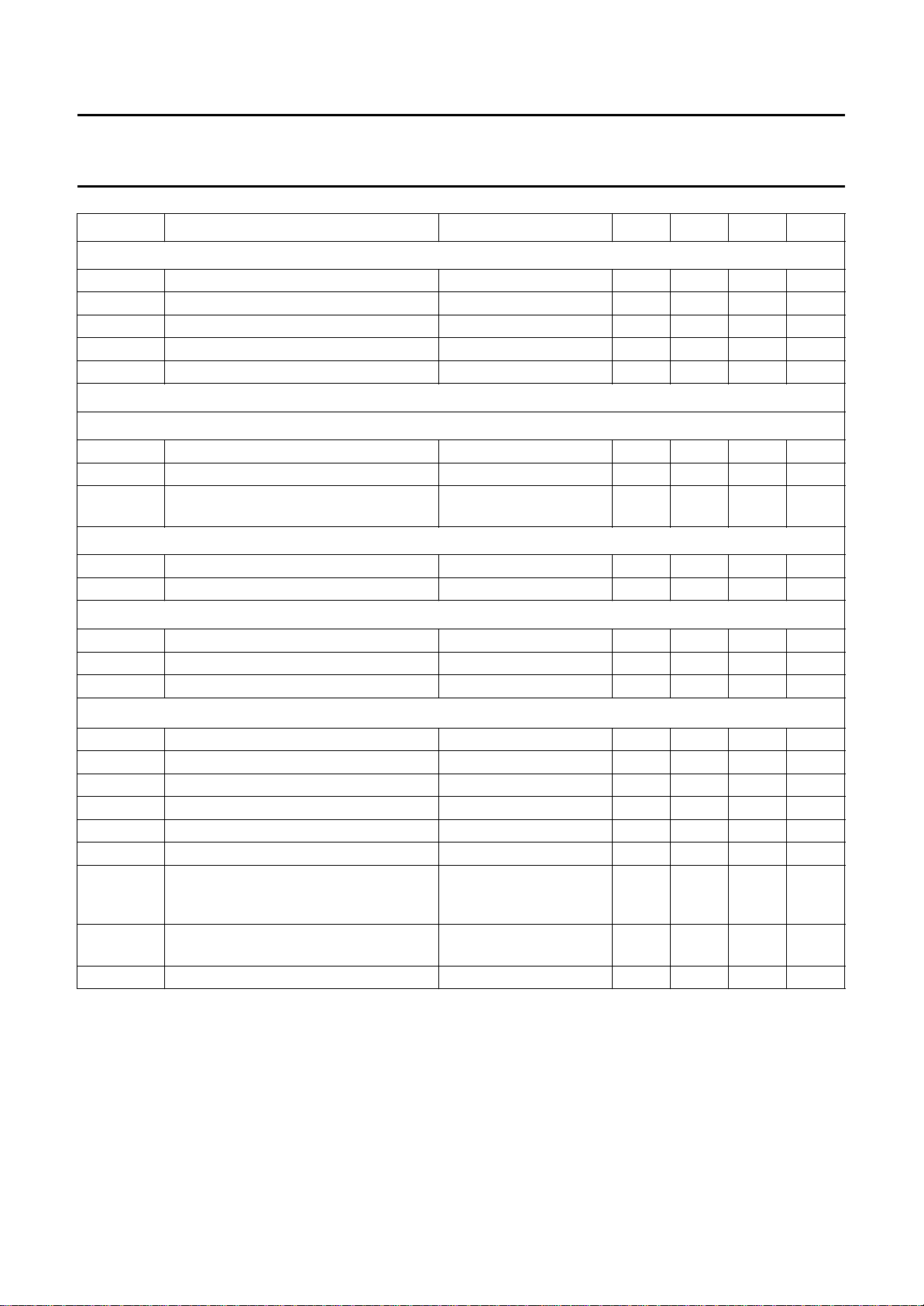
SYMBOL PARAMETER CONDITIONS MIN. TYP. MAX. UNIT
OFY AND OFC INPUTS;3-STATE; see Table 4
V
IL
V
IH
V
I
I
IL
I
IH
Analog-to-digital converter outputs
ANOUTY
V
ANOUT
V
ANOUT
V
ANOUT(p-p)
DIGITAL OUTPUTS Y0 TO Y7, C0 TO C7
V
OL
V
OH
Switching characteristics; see Fig.9
f
clk(max)
t
CPH
t
CPL
Analog signal processing from video input to digital output on both channels; 0 dB gain (f
INL DC integral non-linearity −±0.75 ±1.5 LSB
DNL DC differential non-linearity −±0.4 ±1.0 LSB
AINL AC integral non linearity f
ADNL AC differential non-linearity f
THD total harmonic distortion note 3 −−52 − dB
EB effective bits f
G
diff
ϕ
diff
SVRR2 supply voltage ripple rejection note 6 −−5 %/V
LOW level input voltage 0 − 0.2 V
HIGH level input voltage 2.6 − V
CCD
V
input voltage in high impedance state − 1.15 − V
LOW level input current −370 −300 −µA
HIGH level input current − 500 700 µA
AND ANOUTC OUTPUTS (PINS 16 AND 45); see Table 5
output voltage digital output = 00 − 2.6 − V
output voltage digital output = 255 − 3.6 − V
output voltage amplitude
− 1.0 − V
(peak-to-peak value)
LOW level output voltage IOL=2mA 0 − 0.6 V
HIGH level output voltage IOL= −0.4 mA 2.4 − V
CCD
V
CLK input maximum frequency note 2 30 32 − MHz
clock pulse width HIGH 12 −−ns
clock pulse with LOW 12 −−ns
= 32 MHz)
clk
= 4.43 MHz −±1.5 − LSB
i
= 4.43 MHz −±0.5 − LSB
i
= 4.43 MHz; note 4 − 7.1 − bits
i
differential gain V
= 1.0 V (p-p);
16,45
− 1.5 3.0 %
see Fig.4; PAL
modulated ramp; note 5
differential phase see Fig.5; PAL
− 0.6 1.5 deg
modulated ramp; note 5
1996 Feb 01 9
Page 10
Philips Semiconductors Product specification
YC 8-bit low-power analog-to-digital video
TDA8758
interface
SYMBOL PARAMETER CONDITIONS MIN. TYP. MAX. UNIT
Timing (f
D
IGITAL OUTPUTS (C
t
ds
t
h
t
d
t
W
3-state output delay times; see Fig.10
t
dZH
t
dZL
t
dHZ
t
dLZ
Notes
1. 0 dB is obtained at the AGC amplifier when applying V
2. It is recommended that the rise and fall times of the clock are ≥1 ns. In addition, a ‘good layout’ for the digital and
analog grounds is recommended.
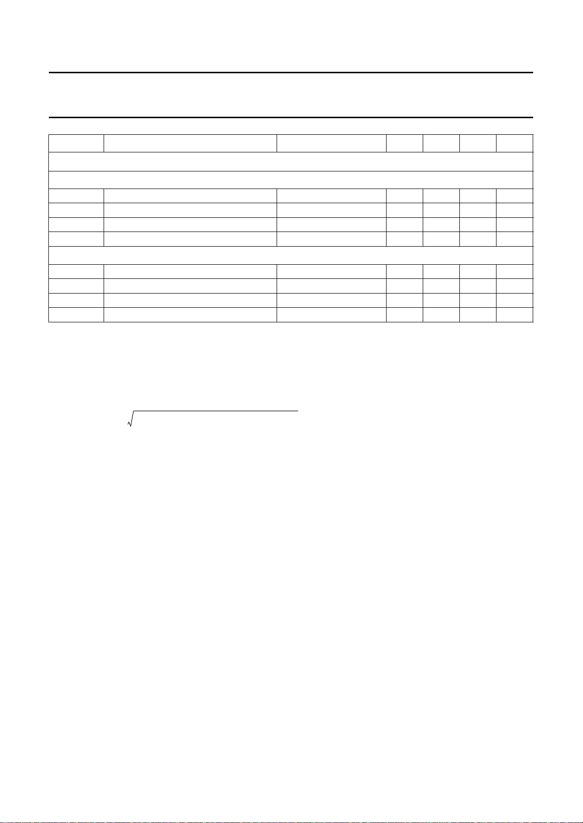
3. THD (total harmonic distortion) is obtained with the addition of the first five harmonics:
THD 20 log
a) F being the fundamental harmonic referenced at 0 dB for a full-scale sine wave input.
4. Effective bits are obtained via a Fast Fourier Transform (FFT) treatment taking 8 K acquisition points per equivalent
fundamental period. The calculation takes into account all harmonics and noise up to half of the clock frequency
(NYQUIST frequency). Conversion to signal-to-noise ratio: S/N = EB × 6.02 + 1.76 dB.
5. Measurement carried out using video analyser VM700A, where video analog signal is reconstructed through a
digital-to-analog converter.
6. The supply voltage ripple rejection is the relative variation of the analog signal (full-scale signal at input) for 0.5 V of
supply variation:
SVRR2
= 32 MHz); see Fig.9
clk
= 15 pF)
L
sampling delay time − 2 − ns
output hold time 10 −−ns
output delay time − 15 18 ns
clamp pulse width see Figs 6 and 7 2 3 −µs
enable HIGH − 12 14 ns
enable LOW − 10 12 ns
disable HIGH − 58 62 ns
disable LOW − 70 74 ns
= 1.0 V on Y channel.
I(p-p)
---------------------------------------------------------------------------------------------------------------=
(2nd)2(3rd)2(4th)2(5th)2(6th)
∆ V
I00()VIFF()
=
-----------------------------------------------------------------------------------------------------
++++
–()V
∆V
F
I00()VIFF()
CCA
2
–()×
1996 Feb 01 10
Page 11
Philips Semiconductors Product specification
YC 8-bit low-power analog-to-digital video
interface
SEL2
handbook, full pagewidth
Y2/CVBS2
Y1/CVBS1
CHROM2
CHROM1
CVBS3
2
4
6
9
11
SEL1
5
C CHANNEL
Y CHANNEL
12
(a)
CHROM2
CHROM1
CVBS3
2
4
6
Y2/CVBS2
Y1/CVBS1
SEL2
5
CHROM2
CHROM1
CVBS3
2
4
6
9
11
SEL1
C CHANNEL
Y CHANNEL
TDA8758
SEL2
5
C CHANNEL
Y CHANNEL
12
(b)
Y2/CVBS2
Y1/CVBS1
9
11
SEL1
12
(c)
MGB471
Fig.3 Video inputs selector.
Table 1 Video input selection
SEL1 SEL2 Y-CHANNEL C-CHANNEL FIGURE 3
0X
(1)
Y1/CVBS1 CHROM1 (a)
1 0 Y2/CVBS2 CHROM2 (b)
1 1 CVBS3 CHROM2 (c)
Note
1. X = don't care.
1996 Feb 01 11
Page 12
Philips Semiconductors Product specification
YC 8-bit low-power analog-to-digital video
interface
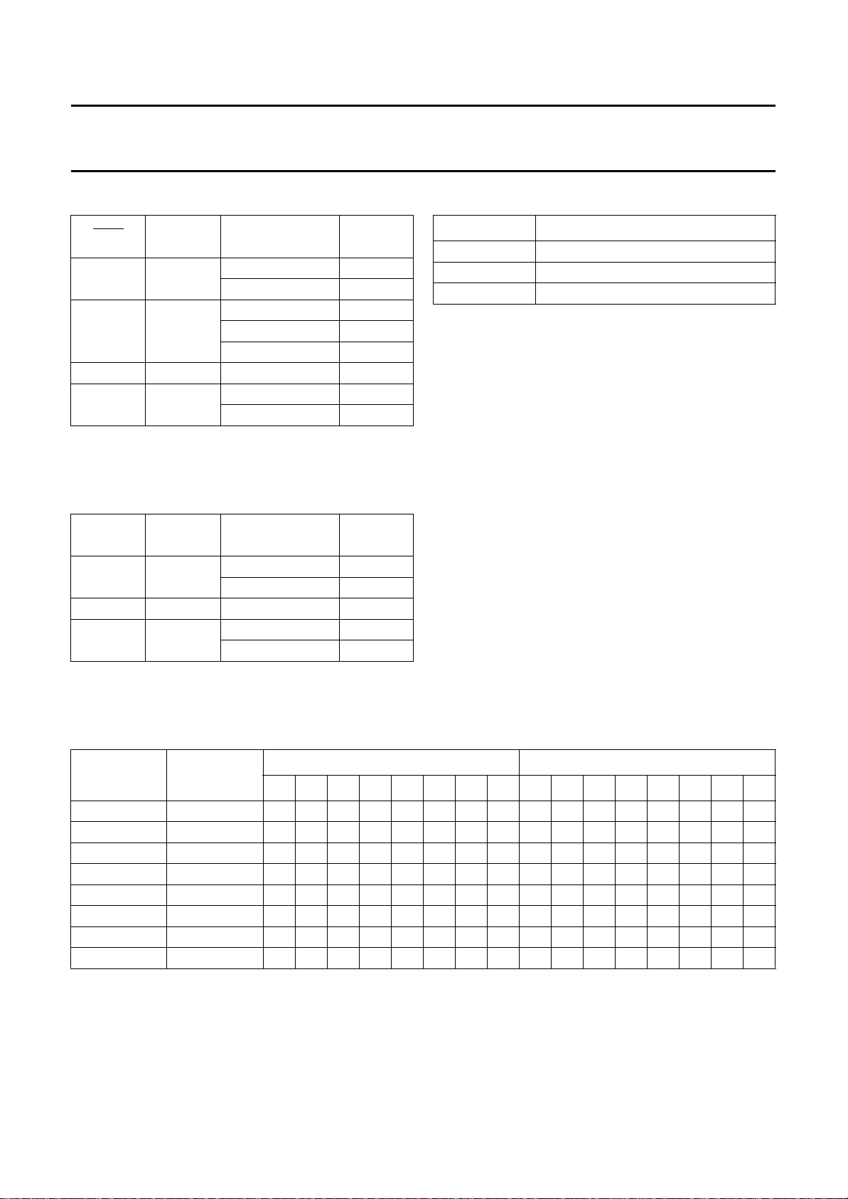
Table 2 AGC output current
PWE GATE A
0 0 output < 255 0 µA
0 1 output < 0+8µA
10X
1 1 output < 0+8µA
Note
1. X = don't care.
Table 3 CLAMP output current
CLAMP GATE B
C 1 output < 128 +54 µA
(1)
X
0X
Y 1 output < 64 +54 µA
DIGITAL
OUTPUT
I
AGC
output > 255 +540 µA
0 < output < 255 −8 µA
output > 255 +540µA
(1)
0 µA
0 < output < 255 −8 µA
DIGITAL
OUTPUT
I
CLAMP
output > 128 −54 µA
(1)
0 µA
64 < output −54 µA
TDA8758
Table 4 OFY and OFC input coding
OFY (or OFC) Y0 to Y7 (or C0 TO C7)
0 active, twos complement
1 high impedance
(1)
open circuit
Note
1. Use C ≥ 10 pF to DGND.
active, binary
Note
1. X = don't care.
Table 5 Output coding and ANOUTY (or ANOUTC) voltage (typical values)
BINARY OUTPUTS TWOS COMPLIMENT
STEP V
I
D7 D6 D5 D4 D3 D2 D1 D0 D7 D6 D5 D4 D3 D2 D1 D0
Underflow − 0000000010000000
0 2.6 0000000010000000
1 − 0000000110000001
. − ................
. − ................
254 − 1111111001111110
255 3.6 1111111101111111
Overflow − 1111111101111111
1996 Feb 01 12
Page 13
Philips Semiconductors Product specification
YC 8-bit low-power analog-to-digital video
interface
handbook, full pagewidth
1.0
DIFFERENTIAL
GAIN
(%)
0.0
1.0
2.0
3.0
(1)
1st 2nd 3rd 4th 5th 6th
(2)
(3)
TDA8758
MBE455
(5)(4)
(6)
step number
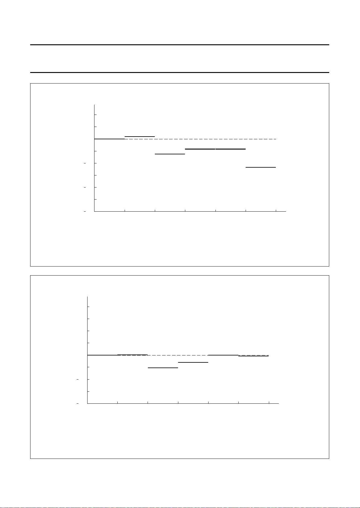
(1) =0.00; (2) = 0.09; (3) = −0.63; (4) = −0.45; (5) = −0.45; (6) = −1.23.
Differential gain = max. (2) − min. (6) = 1.32%.
Fig.4 Typical differential gain result on VM700A.
handbook, full pagewidth
2.0
DIFFERENTIAL
PHASE
(deg)
1.0
(2)
1.0
2.0
(1)
0
1st 2nd 3rd 4th 5th 6th
MBE456
(5)
(4)
(3)
step number
(6)
(1) = 0.00; (2) = 0.03; (3) = −0.53; (4) = −0.32; (5) = 0.01; (6) = −0.08.
Differential phase = max. (2) − min. (3) = 0.56 deg.
1996 Feb 01 13
Fig.5 Typical differential phase result on VM700A.
Page 14
Philips Semiconductors Product specification
YC 8-bit low-power analog-to-digital video
interface
handbook, full pagewidth
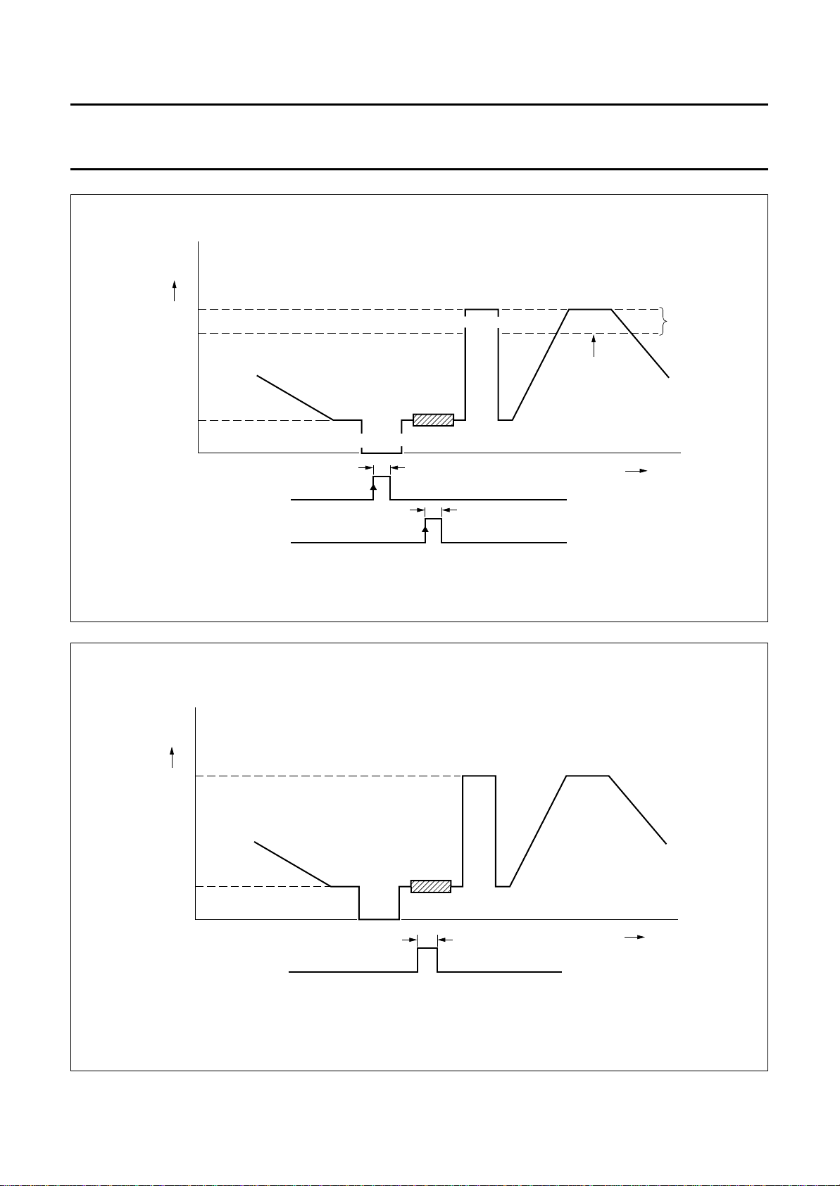
digital
output
level
255
213
black-level
clamping
64
sync-level control
0
GATE A
GATE B
t
W
peak-level gain control
t
W
standard picture
level
TDA8758
safety
margin
time
MGB472
ndbook, full pagewidth
digital
output
level
255
128
Fig.6 Control mode Y channel.
black-level
clamping
0
time
MGB473
GATE B
t
W
1996 Feb 01 14
Fig.7 Control mode C-channel.
Page 15
Philips Semiconductors Product specification
YC 8-bit low-power analog-to-digital video
interface
handbook, full pagewidth
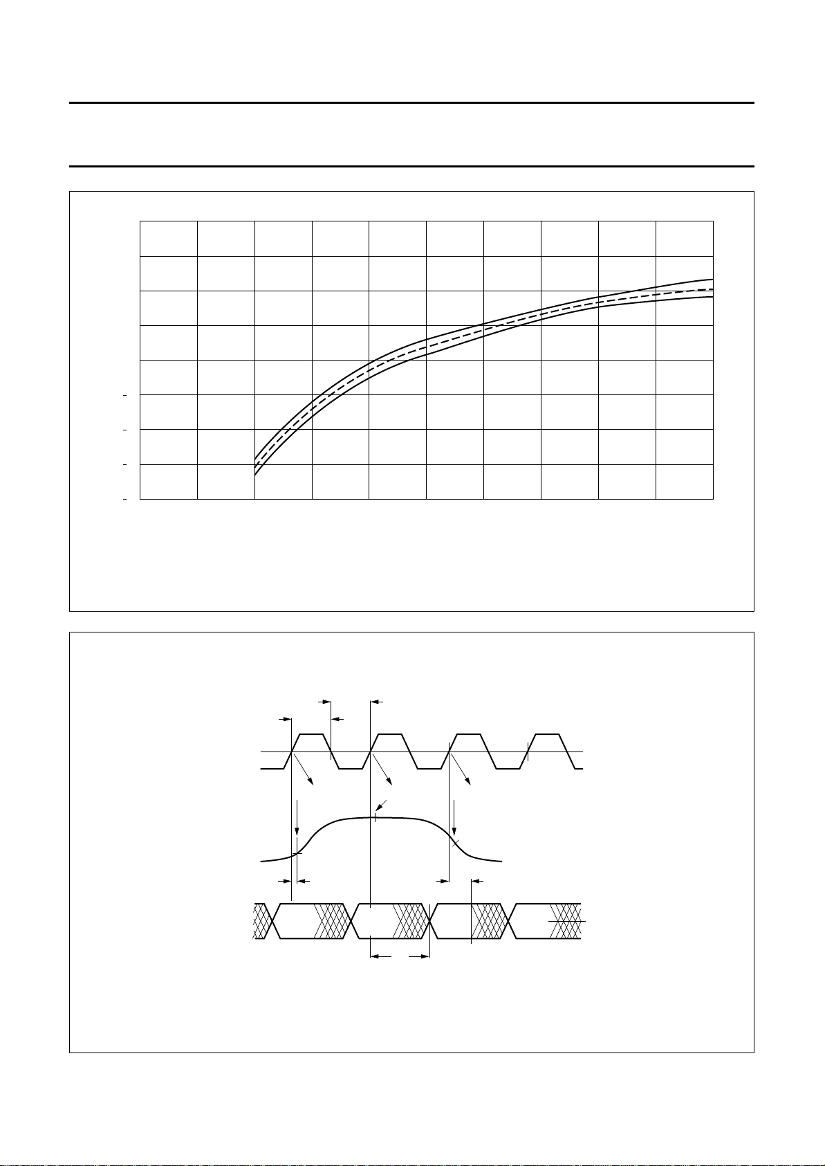
8
AGC
GAIN
(dB)
6
4
2
0
2
4
6
8
3.0 3.2 3.4 3.6 3.8
TDA8758
MBE463
C voltage (V)
AGC
4.03.93.73.53.33.1
Dotted line: Typical curve (T
Full line: Maximum envelope (T
=25°C; VCC= 5 V).
amb
= 0 to 70 °C; VCC= 4.75 to 5.25 V).
amb
Fig.8 AGC behaviour as a function temperature and supply voltage for ANOUTY output; fi= 4.43 MHz, Vi= 0 dB.
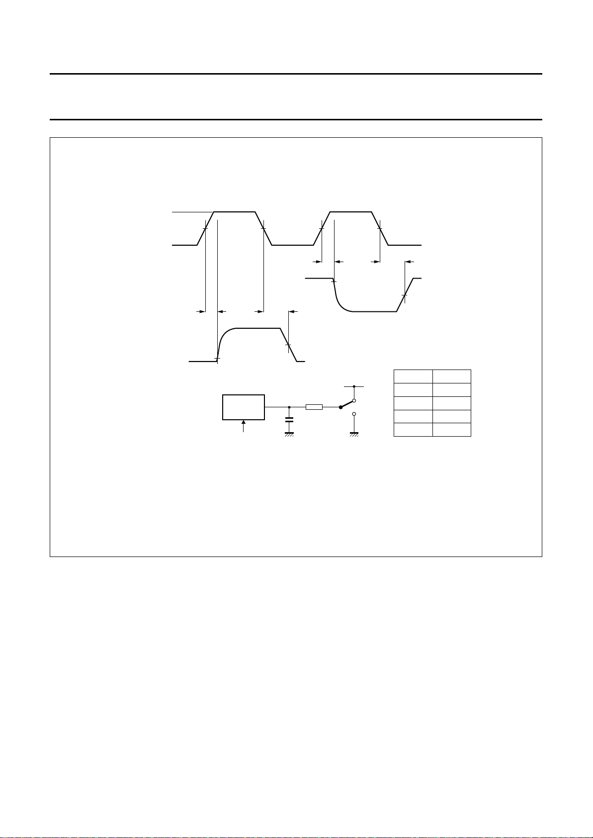
t
handbook, full pagewidth
CLK
V
l
DATA
C0 to C7
Y0 to Y7
t
sample N
DATA
N - 2
CPH
CPL
1.4 V
sample N + 1
t
ds
DATA
N - 1
t
d
sample N + 2
t
h
DATA
N
DATA
N + 1
2.4 V
1.4 V
0.4 V
MBE454
1996 Feb 01 15
Fig.9 Timing diagram.
Page 16
Philips Semiconductors Product specification
YC 8-bit low-power analog-to-digital video
interface
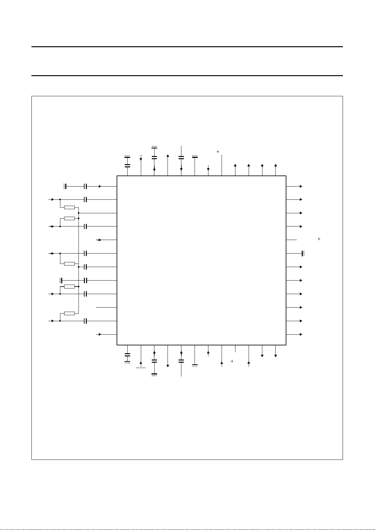
V
handbook, full pagewidth
CCD
OFC
OFY
output
data
output
data
LOW
t
dLZ
10 %
TDA8758
OFC
OFY
HIGH Z
t
dZL
50 %
HIGH
3.3 kΩ
15 pF
t
90 %
dHZ
HIGH Z
V
CCD
S1
50 %
t
dZH
50 %
TEST
t
dLZ
t
dZL
t
dHZ
t
dZH
1.15 V
V
CCD
V
CCD
GND
GND
S1
MBE453
TDA8758
f
OFC=fOFY
= 100 kHz.
Fig.10 Timing diagram and test conditions of 3-state output delay time.
1996 Feb 01 16
Page 17
Philips Semiconductors Product specification
YC 8-bit low-power analog-to-digital video
interface
APPLICATION INFORMATION
V
handbook, full pagewidth
AGND
75 Ω
75 Ω
75 Ω
AGND
75 Ω
75 Ω
22 nF
1 µF
4.7 µF
4.7 µF
18 nF
22 nF
4.7 µF
4.7 µF
C
DEC1
CHROM2
AGND
CHROM1
SEL2
CVBS3
C
CLPY
SDN
Y2/CVBS2
V
CCA
Y1/CVBS1
SEL1
AGND
OFC
CLPC
C
18
nF
48 47 46
1
2
3
4
5
6
7
8
9
10
11
12
13 14 15 16 17 18 19 20 21 22 23 24
470
AGC
nF
PWE
ANOUTC
1 nF
DEC2
DEC3
1 nF
ANOUTY
AGND
CCA
(1)
REG1
45 44 43 42 41 40 39 38 37
REG2
(1)
V
CCA
OGND1
3.3
nF
TDA8758
3.3
GATE A
nF
DGND
V
CCO1
( 5 V)
CLK
( 5 V)
GATE B OFY
C0 C1 C2 C3
V
CCD
TDA8758
36
35
34
33
32
31
30
29
28
27
26
25
Y6Y7
V
MGB476
C4
C5
C6
C7
CCO2
OGND2
Y0
Y1
Y2
Y3
Y4
Y5
( 5 V)
(1) It is recommended that pin 16 and pin 45 are not loaded in order to avoid any distortion.
1996 Feb 01 17
Fig.11 Application diagram.
Page 18
Philips Semiconductors Product specification
YC 8-bit low-power analog-to-digital video
interface
ndbook, full pagewidth
CHROMA IN
LUMA IN
CVBS1 IN
CVBS2 IN
1
2
JP14
3
HEADER 3
3SIP100
PAD100
TEST PT
J10
V
CC
V
CCA
GND
V
CCA
V
CC
PAD100
TEST PT
J9
V
CC
V
CC
C114.7 µF
C130.1 µF
C150.022 µF
C170.022 µF
JP15
HEADER 3
3SIP100
INADCY
INADCC
PAD100
J24
GROUND
V
CX7
0.1 µF
INADCY
1
2
3
CCA
C190.047 µF
GROUND
C274.7 µF
C264.7 µF
C254.7 µF
C120.1 µF
C140.022 µF
C160.022 µF
C180.47 µF
C200.047 µF
V
CC
PAD100
J25
CX13
0.1 µF
11
12
14
19
20
48
46
15
16
45
13
44
17
22
47
V
4
2
9
6
5
7
8
1
CC
U2
CHROMA1
CHROMA2
Y1/CVBS1
Y2/CVBS2
CVBS3
SEL1IN0
SEL2IN1
PWEGPSWO
GATE AHSY
GATE BHCL
CLMP_Y
CLMP_C
SDN
DEC1
DEC2
DEC3
IN_ADC_Y
IN_ADC_CINADCC
AGC_CAP
REG1
REG2
OE_Y
OE_C
4.7 kΩ
R12
22 kΩ
R11
TDA8758
48 37
1
TDA8758
12
13 24
RES
14
11
19
12
17
7
2
1
5
8
U3
LL1 to 5A
LL3A
LFCO
LFCO2
CE
MS
RES
V
DDA
V
DDD
V
DDD
CHR7
CHR6
CHR5
CHR4
CHR3
CHR2
CHR1
CHR0
V
CCO1
V
CCO2
V
V
OGND1
OGND2
DGND
AGND
36
25
CCD
33 CHR7
34 CHR6
35 CHR5
36 CHR4
37 CHR3
38 CHR2
39 CHR1
40 CHR0
23 CVBS7
Y7
24 CVBS6
Y6
25 CVBS5
Y5
26 CVBS4
Y4
27 CVBS3
Y3
28 CVBS2
Y2
29 CVBS1
Y1
30 CVBS0
Y0
42
CLK
41
32
21
10
CCA
31
43
18
3
SAA7197
20SOP300
220 Ω
R13
V
CC
CX3
22 µF
V
CCA
LL1 to 5B
LFCOSEL
CLKREF
PORD
CX12
0.1 µF
LL3B
V
SSA
V
SSD
V
SSD
V
SSD
V
SSD
DEC_LLC
CX14
0.1 µF
CHR0 to 7
CVBS0 to 7
CCX4
0.1 µF
10
20
16
15
3
4
6
9
13
18
CX5
0.1 µF
33 Ω
R15
C24
0.1 µF
CHR7
CHR6
CHR5
CHR4
CHR3
CHR2
CHR1
CHR0
CVBS7
CVBS6
CVBS5
CVBS4
CVBS3
CVBS2
CVBS1
CVBS0
XTAL2
XTAL1
HSY
HCL
DEC_LLC
DEC_REF
LFCO
RES
V
CCA
V
CC
33 Ω
R16
10
26
13
CHR7
12
CHR6
11
CHR5
10
CHR4
9
CHR3
8
CHR2
7
CHR1
6
CHR0
23
CVBS7
22
CVBS6
21
CVBS5
20
CVBS4
17
CVBS3
16
CVBS2
15
CVBS1
14
CVBS0
44
SDAT
33
XTAL
34
XTAL1
24
IN0
GPSW1
25
IN1
GPSW2
29
HSY
26
HCL
27
LL27
4
CREF
36
LFCO
3
RES
37
V
DDA
5
V
DD1
18
V
DD2
28
V
DD3
52
V
DD4
CX6
22 µF
R1433 Ω
1 DEC_LLC
3
5
7
RES
91 61
SAA7151B
27 43
68LLC50U4
SAA7151B
2
DEC_LLC2
4
JP16
HEADER
4X2
8HH100
DEC_CREF
6
8
RES
MBH012
60
44
UV7
UV6
UV5
UV4
UV3
UV2
UV1
UV0
HREF
GTBS
FSI
MUXC
ODD
RTCO
FEIN
GPSWO
RSVRD
IICSA
SDA
SCL
V
SSA
V
SS1
V
SS2
V
SS3
V
SS4
D7
D6
D5
D4
D3
D2
D1
D0
HS
VS
SP
AP
C21
10 pF
C22
10 pF
55
56
57
58
59
60
61
62
45
46
47
48
49
50
53
54
42
31
30
66
68
65
39
32
64
63
39
43
40
41
1
2
35
19
38
51
67
DEC_UV7
DEC_UV6
DEC_UV5
DEC_UV4
DEC_UV3
DEC_UV2
DEC_UV1
DEC_UV0
DEC_Y7
DEC_Y6
DEC_Y5
DEC_Y4
DEC_Y3
DEC_Y2
DEC_Y1
DEC_Y0
GPSWO
TDA8758
DEC_UV0
to 7
DEC_Y0
to 7
DEC_HREF
DEC_HS
DEC_VS
4.7 kΩ
R64
DEC_FI
DEC_RTC
SDA
SCL
V
321
JP5
HEADER 3
3SIP100
Y2
24.576 MHz
2SIP100
C23
0.001 µF
L2
10 µH
CC
XTAL2
XTAL1
1996 Feb 01 18
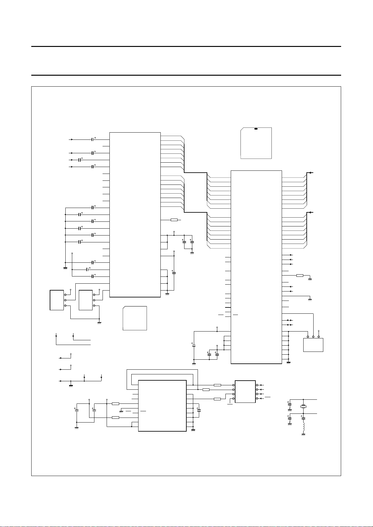
Fig.12 Example of system application (DPC71 evaluation board).
Page 19
Philips Semiconductors Product specification
YC 8-bit low-power analog-to-digital video
interface
PACKAGE OUTLINE
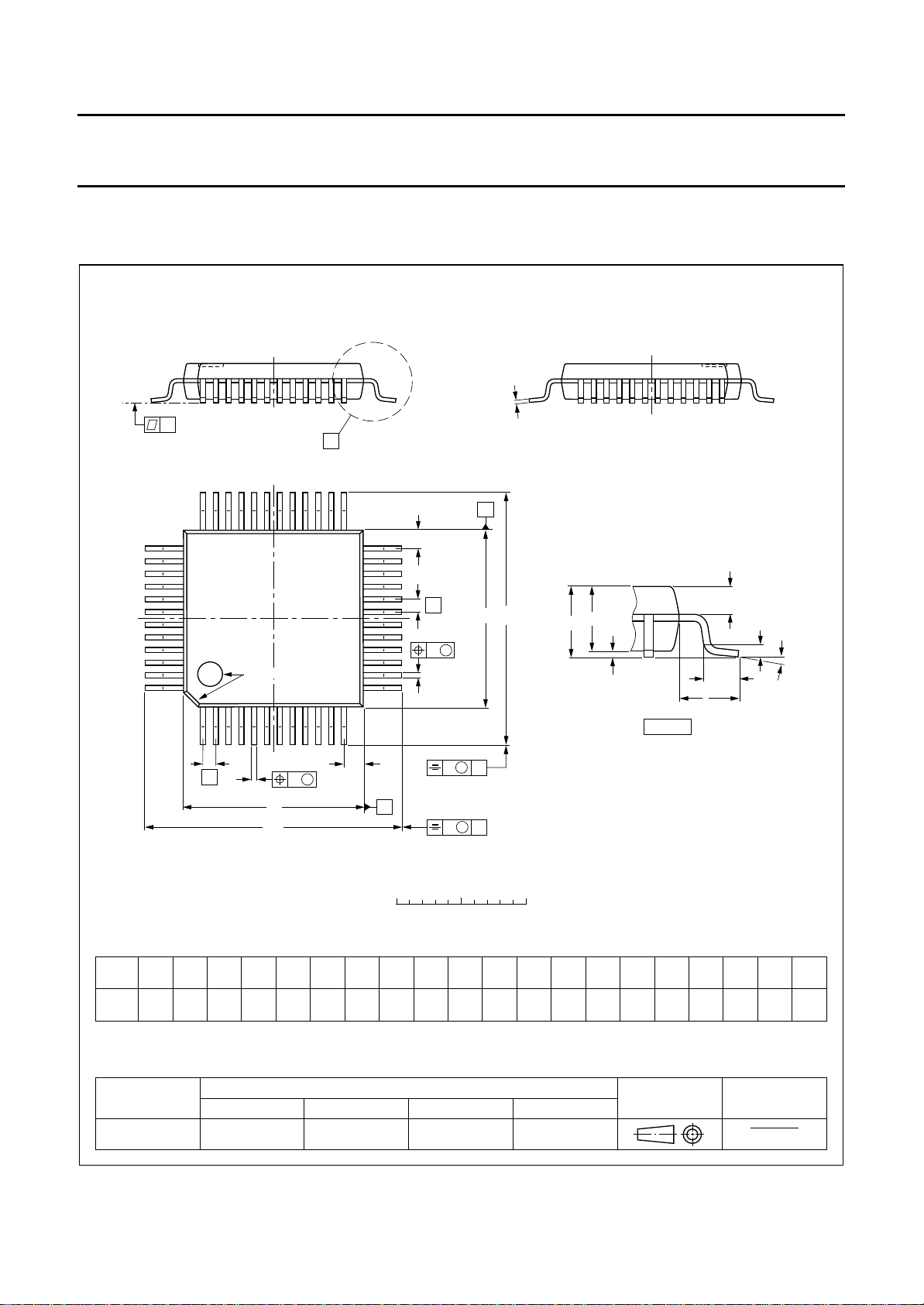
LQFP48: plastic low profile quad flat package; 48 leads; body 7 x 7 x 1.4 mm
c
y
X
36
37
25
Z
24
E
A
TDA8758
SOT313-2
e
w
M
pin 1 index
48
1
e
DIMENSIONS (mm are the original dimensions)
mm
A
A1A2A3b
max.
0.20
1.60
0.05
1.45
1.35
UNIT
Note
1. Plastic or metal protrusions of 0.25 mm maximum per side are not included.
b
p
0.25
w
D
H
D
p
0.27
0.17
12
Z
M
D
(1) (1)(1)
cE
D
0.18
7.1
0.12
6.9
b
p
13
v
B
v
0 2.5 5 mm
scale
(1)
eH
7.1
6.9
0.5
9.15
8.85
H
E
E
M
A
M
B
H
D
LLpQZywv θ
E
9.15
8.85
0.75
0.45
A
2
A
A
1
detail X
0.69
0.59
0.12 0.10.21.0
Q
(A )
3
θ
L
p
L
Z
E
D
0.95
0.55
0.95
0.55
o
7
o
0
OUTLINE
VERSION
SOT313-2
1996 Feb 01 19
REFERENCES
IEC JEDEC EIAJ
EUROPEAN
PROJECTION
ISSUE DATE
93-06-15
94-12-19
Page 20

Philips Semiconductors Product specification
YC 8-bit low-power analog-to-digital video
interface
SOLDERING
Introduction
There is no soldering method that is ideal for all IC
packages. Wave soldering is often preferred when
through-hole and surface mounted components are mixed
on one printed-circuit board. However, wave soldering is
not always suitable for surface mounted ICs, or for
printed-circuits with high population densities. In these
situations reflow soldering is often used.
This text gives a very brief insight to a complex technology.
A more in-depth account of soldering ICs can be found in
our
“IC Package Databook”
Reflow soldering
Reflow soldering techniques are suitable for all LQFP
packages.
Reflow soldering requires solder paste (a suspension of
fine solder particles, flux and binding agent) to be applied
to the printed-circuit board by screen printing, stencilling or
pressure-syringe dispensing before package placement.
Several techniques exist for reflowing; for example,
thermal conduction by heated belt. Dwell times vary
between 50 and 300 seconds depending on heating
method. Typical reflow temperatures range from
215 to 250 °C.
Preheating is necessary to dry the paste and evaporate
the binding agent. Preheating duration: 45 minutes at
45 °C.
Wave soldering
Wave soldering is not recommended for LQFP packages.
This is because of the likelihood of solder bridging due to
closely-spaced leads and the possibility of incomplete
solder penetration in multi-lead devices.
(order code 9398 652 90011).
TDA8758
If wave soldering cannot be avoided, the following
conditions must be observed:
• A double-wave (a turbulent wave with high upward
pressure followed by a smooth laminar wave)
soldering technique should be used.
• The footprint must be at an angle of 45° to the board
direction and must incorporate solder thieves
downstream and at the side corners.
Even with these conditions, do not consider wave
soldering LQFP packages LQFP48 (SOT313-2),
LQFP64 (SOT314-2) or LQFP80 (SOT315-1).
During placement and before soldering, the package must
be fixed with a droplet of adhesive. The adhesive can be
applied by screen printing, pin transfer or syringe
dispensing. The package can be soldered after the
adhesive is cured.
Maximum permissible solder temperature is 260 °C, and
maximum duration of package immersion in solder is
10 seconds, if cooled to less than 150 °C within
6 seconds. Typical dwell time is 4 seconds at 250 °C.
A mildly-activated flux will eliminate the need for removal
of corrosive residues in most applications.
Repairing soldered joints
Fix the component by first soldering two diagonallyopposite end leads. Use only a low voltage soldering iron
(less than 24 V) applied to the flat part of the lead. Contact
time must be limited to 10 seconds at up to 300 °C. When
using a dedicated tool, all other leads can be soldered in
one operation within 2 to 5 seconds between
270 and 320 °C.
1996 Feb 01 20
Page 21

Philips Semiconductors Product specification
YC 8-bit low-power analog-to-digital video
TDA8758
interface
DEFINITIONS
Data sheet status
Objective specification This data sheet contains target or goal specifications for product development.
Preliminary specification This data sheet contains preliminary data; supplementary data may be published later.
Product specification This data sheet contains final product specifications.
Limiting values
Limiting values given are in accordance with the Absolute Maximum Rating System (IEC 134). Stress above one or
more of the limiting values may cause permanent damage to the device. These are stress ratings only and operation
of the device at these or at any other conditions above those given in the Characteristics sections of the specification
is not implied. Exposure to limiting values for extended periods may affect device reliability.
Application information
Where application information is given, it is advisory and does not form part of the specification.
LIFE SUPPORT APPLICATIONS
These products are not designed for use in life support appliances, devices, or systems where malfunction of these
products can reasonably be expected to result in personal injury. Philips customers using or selling these products for
use in such applications do so at their own risk and agree to fully indemnify Philips for any damages resulting from such
improper use or sale.
1996 Feb 01 21
 Loading...