

Page 1

DATA SH EET
Product specification
Supersedes data of June 1994
File under Integrated Circuits, IC02
1995 Mar 09
INTEGRATED CIRCUITS
Philips Semiconductors
TDA8755
YUV 8-bit video low-power
analog-to-digital interface
Page 2
1995 Mar 09 2
Philips Semiconductors Product specification
YUV 8-bit video low-power
analog-to-digital interface
TDA8755
FEATURES
• 8-bit resolution
• Sampling rate up to 20 MHz
• TTL compatible digital inputs
• 3-state TTL outputs
• U, V two's complement outputs
• Y binary output
• Power dissipation of 550 mW (typical)
• Low analog input capacitance, no buffer amplifier
required
• High signal-to-noise ratio over a large analog input
frequency range
• Track-and-hold included
• Clamp functions included
• UV multiplexed ADC
• 4:1:1 output data encoder
• Stable voltage regulator included.
APPLICATIONS
• High speed analog-to-digital conversion for video signal
digitizing
• 100 Hz improved definition TV (IDTV).
GENERAL DESCRIPTION
The TDA8755 is a bipolar 8-bit video low-power
analog-to-digital conversion (ADC) interface for YUV
signals. The device converts the YUV analog input signal
into 8-bit coded digital words in a 4 : 1 : 1 format at a
sampling rate of 20 MHz. The U/V signals are converted in
a multiplexed manner. All analog signal inputs are digitally
clamped and a fast precharge is provided for start-up.
All digital inputs and outputs are TTL compatible. Frame
synchronization is supported in a multiplexed manner.
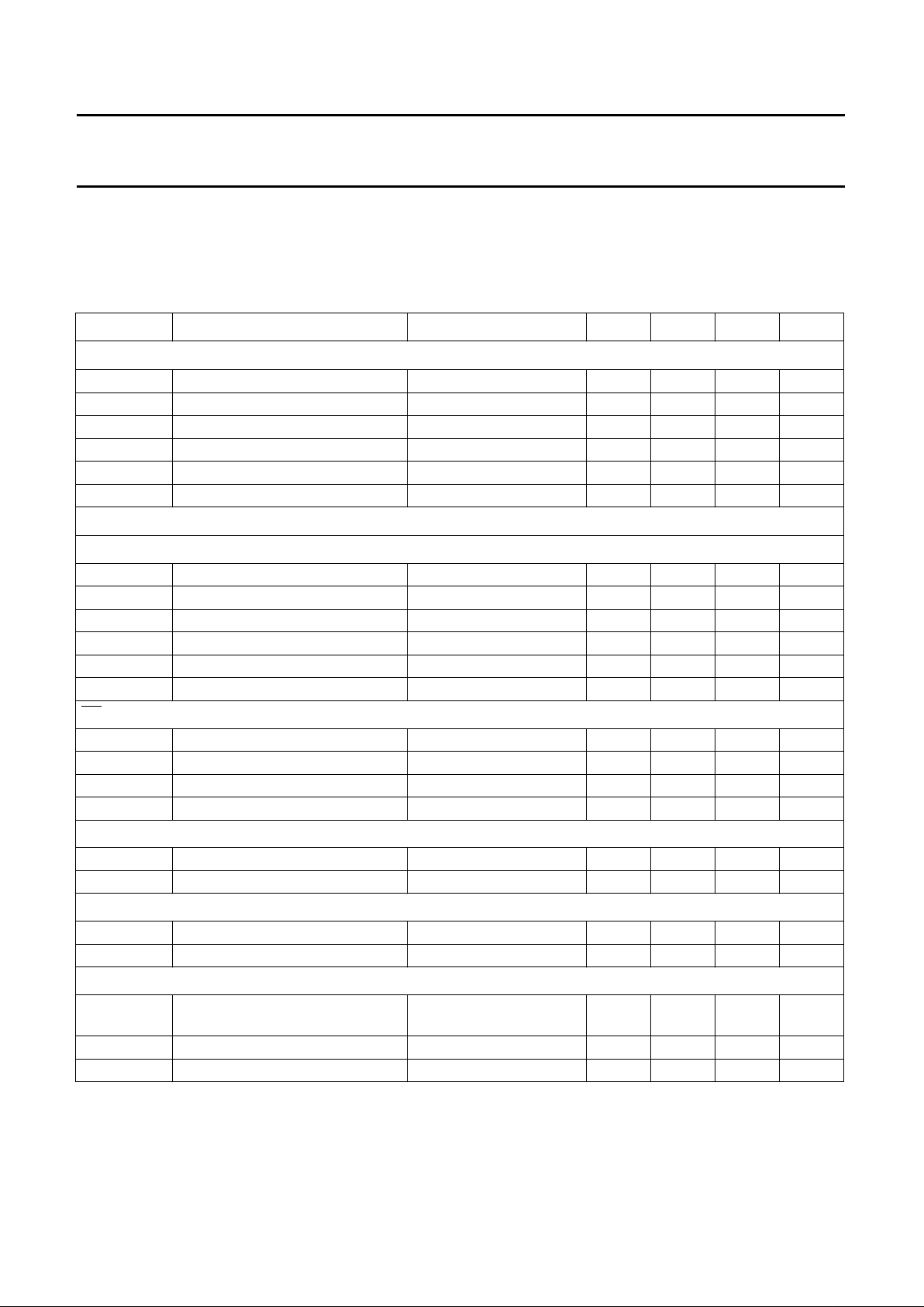
QUICK REFERENCE DATA
ORDERING INFORMATION
SYMBOL PARAMETER CONDITIONS MIN. TYP. MAX. UNIT
V
CCA
analog supply voltage 4.75 5.0 5.25 V
V
CCD
digital supply voltage 4.75 5.0 5.25 V
V
CCO
output stages supply voltage 4.75 5.0 5.25 V
I
CCA
analog supply current − 46 55 mA
I
CCD
digital supply current − 55 66 mA
I
CCO
output stages supply current − 912mA
INL DC integral non-linearity f
clk
= 2 MHz −±0.4 ±1 LSB
DNL DC differential non-linearity f
clk
= 2 MHz −±0.3 ±0.5 LSB
EB effective bits − 7.1 − bits
f
clk(max)
maximum clock frequency 20 −−MHz
P
tot
total power dissipation − 550 700 mW
TYPE NUMBER
PACKAGE
PINS PIN POSITION MATERIAL CODE
TDA8755T 32 SO32L plastic SOT287-1
Page 3
1995 Mar 09 3
Philips Semiconductors Product specification
YUV 8-bit video low-power
analog-to-digital interface
TDA8755
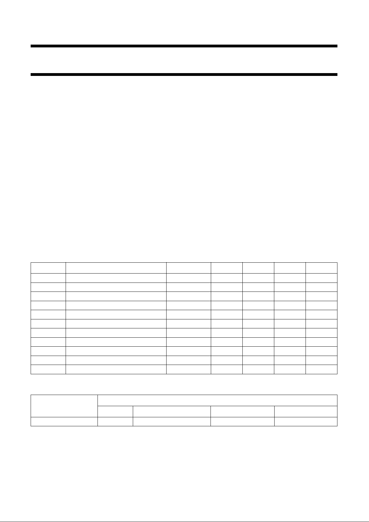
BLOCK DIAGRAM
handbook, full pagewidth
MLA734 - 1
CLAMPUCLAMP
V
DIGITAL
MULTIPLEXER
TRACK
AND
HOLD
TRACK
AND
HOLD
ANALOG
MULTIPLEXER
TRACK
AND
HOLD
8-BIT
ADC
COMPARATOR
128
U AND V
DATA
ENCODER
TTL
I / O
TIMING GENERATOR
SUPPLY AND REFERENCE
VOLTAGE REGULATOR
CLAMP
LOGIC
8
TRACK
AND
HOLD
8-BIT
ADC
COMPARATOR
16
8-BIT
PIPELINE
TTL
I / O
8
CLAMP
Y
12
9
INV
CLPV
CLPU
11
7
INU
CLP
CLPY
INY
15
5
3
6 322310188 1
V
CCA
V
CCD
V
CCO AGND DGND SDN n.c.
192021
22
17
14
16
CLK
CE
HREF
2
D'0
D'1
D'2
D'3
U
V
2
D0
D7
Y
24
31
8
REG1 REG2 REG3
2413
8
TDA8755
Fig.1 Block diagram.
Page 4
1995 Mar 09 4
Philips Semiconductors Product specification
YUV 8-bit video low-power
analog-to-digital interface
TDA8755
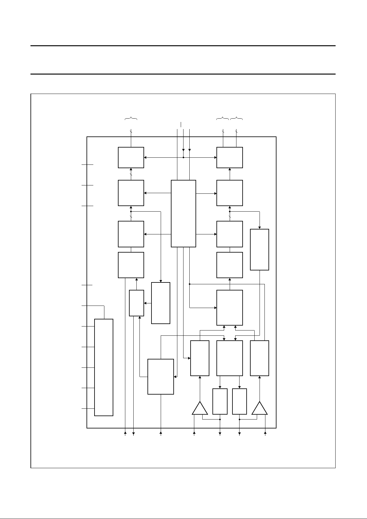
PINNING
SYMBOL PIN DESCRIPTION
n.c. 1 not connected
REG1 2 decoupling input (internal
stabilization loop decoupling)
INY 3 Y analog voltage input
REG2 4 decoupling input (internal
stabilization loop decoupling)
CLPY 5 Y clamp capacitor connection
V
CCA
6 analog positive supply voltage
(+5 V)
INU 7 U analog voltage input
SDN 8 stabilizer decoupling node and
analog reference voltage (+3.35 V)
INV 9 V analog voltage input
AGND 10 analog ground
CLPU 11 U clamp capacitor connection
CLPV 12 V clamp capacitor connection
REG3 13 decoupling input (internal
stabilization loop decoupling)
CE 14 chip enable input (TTL level input
active LOW)
CLP 15 clamp control input
HREF 16 horizontal reference signal
CLK 17 clock input
DGND 18 digital ground
D'0 19 V data output; bit 0 (n−1)
D'1 20 V data output; bit 1 (n)
D'2 21 U data output; bit 0 (n−1)
D'3 22 U data output; bit 1 (n)
V
CCO
23 positive supply voltage for output
stages (+5 V)
D0 24 Y data output; bit 0 (LSB)
D1 25 Y data output; bit 1
D2 26 Y data output; bit 2
D3 27 Y data output; bit 3
D4 28 Y data output; bit 4
D5 29 Y data output; bit 5
D6 30 Y data output; bit 6
D7 31 Y data output; bit 7 (MSB)
V
CCD
32 digital positive supply voltage (+5 V)
Fig.2 Pin configuration.
handbook, halfpage
1
2
3
4
5
6
7
8
9
10
11
12
13
14
15
16
32
31
30
29
28
27
17
18
19
20
21
22
23
24
25
26
TDA8755
n.c.
REG1
INY
REG2
CLPY
V
CCA
INU
SDN
INV
AGND
CLPU
CLPV
REG3
CE
CLP
HREF CLK
DGND
D'0
D'1
D'2
D'3
V
CCO
D0
D1
D2
D3
D4
D5
D6
D7
V
CCD
MLA728 - 1
Page 5
1995 Mar 09 5
Philips Semiconductors Product specification
YUV 8-bit video low-power
analog-to-digital interface
TDA8755
LIMITING VALUES
In accordance with the Absolute Maximum Rating System (IEC134).
HANDLING
Inputs and outputs are protected against electrostatic discharges in normal handling. However, to be totally safe, it is
desirable to take normal precautions appropriate to handling integrated circuits.
THERMAL CHARACTERISTICS
SYMBOL PARAMETER CONDITIONS MIN. MAX. UNIT
V
CCA
analog supply voltage −0.3 +7.0 V
V
CCD
digital supply voltage −0.3 +7.0 V
V
CCO
output stages supply voltage −0.3 +7.0 V
∆V
CC
supply voltage difference between V
CCA
and V
CCD
−1.0 +1.0 V
supply voltage difference between V
CCO
and V
CCD
−1.0 +1.0 V
supply voltage difference between V
CCA
and V
CCO
−1.0 +1.0 V
V
I
input voltage referenced to AGND − +5.0 V
V
clk(p-p)
AC input voltage for switching (peak-to-peak value) referenced to DGND − V
CCD
V
I
O
output current − +6 mA
T
stg
storage temperature −55 +150 °C
T
amb
operating ambient temperature 0 +70 °C
T
j
junction temperature − +150 °C
SYMBOL PARAMETER VALUE UNIT
R
th j-a
thermal resistance from junction to ambient in free air 70 K/W
Page 6
1995 Mar 09 6
Philips Semiconductors Product specification
YUV 8-bit video low-power
analog-to-digital interface
TDA8755
CHARACTERISTICS
V
CCA=V6
to V10= 4.75 to 5.25 V; V
CCD=V32
to V18= 4.75 to 5.25 V; V
CCO=V23
to V18= 4.75 to 5.25 V;
AGND and DGND shorted together; V
CCA
to V
CCD
= −0.25 to +0.25 V; V
CCO
to V
CCD
= −0.25 to +0.25 V;
V
CCA
to V
CCO
= −0.25 to +0.25 V; T
amb
= 0 to +70 °C; typical values measured at V
CCA=VCCD=VCCO
= 5 V and
T
amb
=25°C; unless otherwise specified.
SYMBOL PARAMETER CONDITIONS MIN. TYP. MAX. UNIT
Supply
V
CCA
analog supply voltage 4.75 5.0 5.25 V
V
CCD
digital supply voltage 4.75 5.0 5.25 V
V
CCO
output stages supply voltage 4.75 5.0 5.25 V
I
CCA
analog supply current − 46 55 mA
I
CCD
digital supply current − 55 66 mA
I
CCO
output stages supply current − 912mA
Inputs
CLK (
PIN 17)
V
IL
LOW level input voltage 0 − 0.8 V
V
IH
HIGH level input voltage 2.0 − V
CCD
V
I
IL
LOW level input current V
clk
= 0.4 V −400 −−µA
I
IH
HIGH level input current V
clk
= 2.7 V −−100 µA
Z
I
input impedance f
clk
=20MHz − 4 − kΩ
C
I
input capacitance f
clk
=20MHz − 4.5 − pF
CE, CLP AND HREF (PINS 14 TO 16)
V
IL
LOW level input voltage 0 − 0.8 V
V
IH
HIGH level input voltage 2.0 − V
CCD
V
I
IL
LOW level input current V
clk
= 0.4 V −400 −−µA
I
IH
HIGH level input current V
clk
= 2.7 V −−100 µA
CLPY (PIN 5)
V
5
clamp voltage for 16 output code − 3.725 − V
I
5
clamp output current −±50 −µA
CLPU AND CLPV (PINS 11 AND 12)
V
11, 12
clamp voltage for 128 output code − 3.30 − V
I
11, 12
clamp output current −±50 −µA
INY (PIN 3)
V
I(p-p)
input voltage, full range
(peak-to-peak value)
fi= 4.43 MHz 0.93 1.0 1.07 V
Z
I
input impedance fi= 6 MHz − 30 − kΩ
C
I
input capacitance fi= 6 MHz − 1 − pF
Page 7

1995 Mar 09 7
Philips Semiconductors Product specification
YUV 8-bit video low-power
analog-to-digital interface
TDA8755
INU AND INV (PINS 7 AND 9)
V
I(p-p)
input voltage, full range
(peak-to-peak value)
fi= 1.5 MHz 0.93 1.03 1.13 V
Z
I
input impedance fi= 2 MHz − 30 − kΩ
C
I
input capacitance fi= 2 MHz − 1 − pF
INPUTS ISOLATION
α
ct
crosstalk between Y, U and V −−55 −50 dB
Outputs
SDN (
PIN 8)
V
ref
reference voltage − 3.32 − V
V
REG
line regulation 4.75 V ≤ V
CCA
≤ 5.25 V − 4.0 − mV
I
L
load current −2 −−mA
DIGITAL OUTPUTS D0 TO D7 AND D’0 TO D’3 (PINS 24 TO 31 AND 19 TO 22)
V
OL
LOW level output voltage IO= 0.4 mA 0 − 0.4 V
I
O
= 1.5 mA 0 − 0.5 V
V
OH
HIGH level output voltage IO= −0.4 mA 2.4 − V
CCD
V
I
OZ
output current in 3-state mode 0.4 V < VO<V
CCD
−20 − +20 µA
Switching characteristics
f
clk(max)
maximum clock frequency 20 −−MHz
f
clk(min)
minimum clock frequency −−2.0 MHz
t
CPH
clock pulse width HIGH 20 −−ns
t
CPL
clock pulse width LOW 20 −−ns
Analog signal processing (f
clk
= 20 MHz; 50% clock duty factor)
G
diff
differential gain note 1; see Fig.8 − 2 − %
ϕ
diff
differential phase note 1; see Fig.8 − 3 − deg
f
1
fundamental harmonics (full-scale) note 2 −−0dB
f
all
harmonics (full-scale),
all components
note 2; see Fig.10 −−54 − dB
SVRR1 supply voltage ripple rejection 1 note 3 −−40 − dB
SVRR2 supply voltage ripple rejection 2 note 3 − 1.0 − %/V
Transfer function (50% clock duty factor)
INL DC integral non-linearity f
clk
= 2 MHz −±0.4 ±1.0 LSB
DNL DC differential non-linearity f
clk
= 2 MHz −±0.3 ±0.5 LSB
AILE AC integral non-linearity note 4 −±1.0 ±2.0 LSB
EB effective bits note 5; Fig.10 − 7.1 − bits
SYMBOL PARAMETER CONDITIONS MIN. TYP. MAX. UNIT
Page 8

1995 Mar 09 8
Philips Semiconductors Product specification
YUV 8-bit video low-power
analog-to-digital interface
TDA8755
Notes
1. Low frequency ramp signal (V
I(p-p)
= full-scale and 64 µs period) combined with a sinewave input voltage
(V
I(p-p)
= 0.25 full-scale, fi= maximum permitted frequency) at the input.
2. The input conditions are related as follows:
a) Y channel: V
I(p-p)
= 1.0 V; fi= 4.43 MHz
b) U/V channel: V
I(p-p)
= 1.0 V; fi= 1.5 MHz.
3. Supply voltage ripple rejection:
a) SVRR1 is the variation of the input voltage producing output code 127 (code 15) for supply voltage variation
of 0.5 V:
b) SVRR2 is the relative variation of the full-scale range of analog input for a supply voltage variation of 0.5 V:
4. Full-scale sinewave (f
i
= 4.43 MHz for Y and fi= 1.5 MHz for U and V; f
clk
= 20 MHz).
5. The number of effective bits is measured using a 20 MHz clock frequency. This value is given for a 4.43 MHz input
frequency on the Y channel (1.5 MHz on the U and V channels). This value is obtained via a Fast Fourier Transform
(FFT) treatment taking 4 × T
clk
(clock periods) acquisition points per period. The calculation takes into account all
harmonics and noise up to half of the clock frequency (NYQUIST frequency).
Conversion to signal-to-noise ratio: S/N = EB × 6.02 + 1.76 dB.
6. Output data acquisition is available after the maximum delay time of td.
7. U and V output data is not valid during t
CLP
.
Timing (f
clk
= 20 MHz); note 6; see Figs 3 to 7
t
ds
sampling delay time − 1 − ns
t
h
output hold time 7 −−ns
t
d
output delay time − 33 42 ns
t
dZH
3-state output delay time enable-to-HIGH − 10 14 ns
t
dZL
3-state output delay time enable-to-LOW − 10 14 ns
t
dHZ
3-state output delay time disable-to-HIGH − 811ns
t
dLZ
3-state output delay time disable-to-LOW − 46ns
t
r
clock rise time 3 5 − ns
t
f
clock fall time 3 5 − ns
t
su
HREF set-up time 7 −−ns
t
h
HREF hold time 3 −−ns
t
r
data output rise time − 12 − ns
t
f
data output fall time − 16 − ns
t
CLP
minimum time for active clamp note 7; see Fig.9 3 −−µs
SYMBOL PARAMETER CONDITIONS MIN. TYP. MAX. UNIT
SVRR1 20 log
∆V
I127()
∆V
CCA
----------------------
=
SVVR2
∆ V
I0()VI255()
–()
V
I0()VI 255()
–
------------------------------------------------
1
∆ V
CCA
------------------
×=
Page 9

1995 Mar 09 9
Philips Semiconductors Product specification
YUV 8-bit video low-power
analog-to-digital interface
TDA8755
Table 1 Mode selection
Table 2 Output data coding
CE D7 TO D0; D’3 TO D’0
1 high impedance
0 active; binary
OUTPUT PORT BIT OUTPUT DATA
YD7Y
0
7Y
1
7Y
2
7Y
3
7
D6 Y
0
6Y
1
6Y
2
6Y
3
6
D5 Y
0
5Y
1
5Y
2
5Y
3
5
D4 Y
0
4Y
1
4Y
2
4Y
3
4
D3 Y
0
3Y
1
3Y
2
3Y
3
3
D2 Y
0
2Y
1
2Y
2
2Y
3
2
D1 Y
0
1Y
1
1Y
2
1Y
3
1
D0 Y
0
0Y
1
0Y
2
0Y
3
0
U D’3
U07U
0
5U
0
3U
0
1
D’2 U
0
6U
0
4U
0
2U
0
0
V D’1
V07V
0
5V
0
3V
0
1
D’0 V
0
6V
0
4V
0
2V
0
0
Fig.3 Timing diagram (INY signal).
ndbook, full pagewidth
ds
t
sample N 1
sample N
CLK
MSA646
sample N 2 sample N 3 sample N 4 sample N 5
1.4 V
V
l
D0 to D7
t
d
t
h
2.4 V
0.4 V
1.4 V
DATA
N 1
DATA
N
DATA
N 1
DATA
N 2
DATA
N 3
DATA
N 4
t
CPHtCPL
Page 10

1995 Mar 09 10
Philips Semiconductors Product specification
YUV 8-bit video low-power
analog-to-digital interface
TDA8755
ndbook, full pagewidth
MBD874
50 %
50 %
HIGH
LOW
dZH
t
dHZ
t
50 %
HIGH
LOW
dZL
t
dLZ
t
10 %
90 %
output
data
V
CCD
output
data
3.3 kΩ
15 pF
S1
V
CCD
TDA8755
CE
CE
Fig.4 Timing diagram and test conditions of 3-state output delay time.
TEST S1
t
dLZ
V
CCD
t
dZL
V
CCD
t
dHZ
GND
t
dZH
GND
fCE= 100kHz.
Fig.5 Load circuit for the 3-state output timing
measurement.
handbook, halfpage
MLA733 - 1
15 pF
test probe
TEK P6201
D0 to D7
TDA8755
Page 11

1995 Mar 09 11
Philips Semiconductors Product specification
YUV 8-bit video low-power
analog-to-digital interface
TDA8755
Fig.6 Timing definition for set-up and hold times (HREF signal).
The output data is valid 4 clock periods after HREF goes HIGH.
handbook, full pagewidth
MLA732 - 1
CLK
HREF
output
data
output data valid
123
4
t
h
t
su
sample N
N 4 N 3 N 2 N 1 N
sample N
sample N 4
5
Fig.7 Timing diagram (HREF signal).
When the HREF period is a multiple of 4 clock periods, the output data is valid without any clock delay.
The internal circuit always gives an internal delay of 4 clock periods as illustrated in Fig.6.
handbook, full pagewidth
MLA731 - 1
CLK
HREF
output
data
output data valid
4 clock periods (T )
sample N sample N 4 x T
N 4 N 3 N 3
sample N 4 (T 1)
clk
clk
clk
Page 12

1995 Mar 09 12
Philips Semiconductors Product specification
YUV 8-bit video low-power
analog-to-digital interface
TDA8755
Fig.8 Input test signal for differential gain and phase measurements.
Y channel = 4.43 MHz sinewave.
U, V channel = 1.5 MHz sinewave.
handbook, full pagewidth
MSA644
64 µs
0.3 V
Y, U and V
channel
1.2 V
0.3 V
Fig.9 Clamping control timing.
handbook, full pagewidth
MSA645
digital
output
level
255
0
time
black-level
clamping
CLP
Y : 16
U,V : 128
CLP
t
Page 13

1995 Mar 09 13
Philips Semiconductors Product specification
YUV 8-bit video low-power
analog-to-digital interface
TDA8755
Fig.10 Fast Fourier Transform (f
clk
= 20 MHz; fi= 4.43 MHz).
Effective bits: 7.30; THD = −53.35 dB.
Harmonic levels (dB): 2nd = −58.38; 3rd = −60.03; 4th = −57.30; 5th = −69.38; 6th = −67.09.
handbook, full pagewidth
3.75
0
120
0 1.25 2.50
MBD873
40
80
8.755.00 6.25 7.50 10.00
f (MHz)
100
20
60
amplitude
(dB)
Page 14

1995 Mar 09 14
Philips Semiconductors Product specification
YUV 8-bit video low-power
analog-to-digital interface
TDA8755
APPLICATION INFORMATION
Fig.11 Application diagram.
The analog and digital supplies should be separated and decoupled.
(1) Clamp capacitors must be determined in accordance with the application; recommended values are CLPY = 18 nF, CLPU and CLPV = 33 nF.
(2) It is possible to use the reference output voltage pin SDN to drive other analog circuits under the limits indicated in Chapter “Characteristics”.
(3) Input signal pins have a high bandwidth. It is necessary to take special care on PCB layout to avoid any interaction from other signals (digital clocks
for example).
ndbook, full pagewidth
1
2
3
4
5
6
7
8
9
10
11
12
13
14
15
16
32
31
30
29
28
27
17
18
19
20
21
22
23
24
25
26
TDA8755
n.c.
REG1
INY
220 nF
AGND
AGND
REG2
CLPY
V
CCA
INU
5 V
10 nF
SDN
INV
AGND
CLPU
CLPV
REG3
CLP
HREF
CE
220 nF
AGND
AGND
AGND
MLA735 - 1
CLK
DGND
D'0
D'1
D'2
D'3
V
CCO
D0
D1
D2
D3
D4
D5
D6
D7
V
CCD
DGND
DGND
10 nF
10 nF
AGND
10 nF
4.7 µF
4.7 µF
4.7 µF
10 nF
+ 3.35 V
(2)
(1)
(1)
5 V
5 V
(1)
(3)
(3)
(3)
Page 15

1995 Mar 09 15
Philips Semiconductors Product specification
YUV 8-bit video low-power
analog-to-digital interface
TDA8755
Fig.12 Block diagram of a full-options Improved Picture Quality (IPQ) module.
ndbook, full pagewidth
MSA642
Y
U
V
12
VDRAM
1 x TMS4C2970
VDRAM
1 x TMS4C2970
12
12
SAA4940
NOISE
REDUCTION
INCLUDING
CROSS-COLOUR
REDUCTION
12
12
VIDEO
ENHANCEMENT,
LFR
PROCESSING
AND DACs
SAA7158 Y
U
V
to
video
processor
22
12
VCO2A
VCO2B
MEMORY
CONTROLLER
SAA4951
control
VCO1
12/13.5/16/18 MHz 32/36 MHz
VSYNC
SC1
MICROCONTROLLER
PCB83C652
control
data
8
2
µC bus
I C
2
H2, V2
(32 kHz/100 Hz)
27 MHz
to
deflection
processor
2
TDA8755
Page 16

1995 Mar 09 16
Philips Semiconductors Product specification
YUV 8-bit video low-power
analog-to-digital interface
TDA8755
Fig.13 Block diagram of an economic Improved Picture Quality (IPQ) module.
ndbook, full pagewidth
MSA643
Y
U
V
12 12
VIDEO
ENHANCEMENT
AND
DACs
SAA7165
Y
U
V
to
video
processor
2
VCO2A
VCO2B
MEMORY
CONTROLLER
SAA4951
control
VCO1
12/13.5/16/18 MHz 32/36 MHz
VSYNC
SC1
MICROCONTROLLER
PCB83C652
control
data
8
I C
2
H2, V2
(32 kHz/100 Hz)
27 MHz
to
deflection
processor
VDRAM
1 x
TMS4C2970
2
I C bus
2
TDA8755
Page 17

1995 Mar 09 17
Philips Semiconductors Product specification
YUV 8-bit video low-power
analog-to-digital interface
TDA8755
PACKAGE OUTLINE
handbook, full pagewidth
UNIT
A
max.
A1A
2
A3b
p
cD
(1)E(1)
eHELLpQZywv θ
REFERENCES
OUTLINE
VERSION
EUROPEAN
PROJECTION
ISSUE DATE
IEC JEDEC EIAJ
mm
inches
2.65
0.10
0.25
0.01
1.4
0.055
0.3
0.1
2.45
2.25
0.49
0.36
0.27
0.18
20.7
20.3
7.6
7.4
1.27
10.65
10.00
1.2
1.0
0.95
0.55
8
0
o
o
0.25 0.1
0.004
0.25
DIMENSIONS (inch dimensions are derived from the original mm dimensions)
Note
1. Plastic or metal protrusions of 0.15 mm maximum per side are not included.
1.1
0.4
SOT287-1
92-11-17
95-01-25
(1)
0.012
0.004
0.096
0.086
0.02
0.01
0.050
0.047
0.039
0.42
0.39
0.30
0.29
0.81
0.80
0.011
0.007
0.037
0.022
0.010.01
0.043
0.016
w M
b
p
D
H
E
Z
e
c
v M
A
X
A
y
32
17
16
1
θ
A
A
1
A
2
L
p
Q
detail X
L
(A )
3
E
pin 1 index
0 5 10 mm
scale
SO32: plastic small outline package; 32 leads; body width 7.5 mm
SOT287-1
Page 18

1995 Mar 09 18
Philips Semiconductors Product specification
YUV 8-bit video low-power
analog-to-digital interface
TDA8755
SOLDERING
Plastic small outline packages
B
YWAVE
During placement and before soldering, the component
must be fixed with a droplet of adhesive. After curing the
adhesive, the component can be soldered. The adhesive
can be applied by screen printing, pin transfer or syringe
dispensing.
Maximum permissible solder temperature is 260 °C, and
maximum duration of package immersion in solder bath is
10 s, if allowed to cool to less than 150 °C within 6 s.
Typical dwell time is 4 s at 250 °C.
A modified wave soldering technique is recommended
using two solder waves (dual-wave), in which a turbulent
wave with high upward pressure is followed by a smooth
laminar wave. Using a mildly-activated flux eliminates the
need for removal of corrosive residues in most
applications.
B
Y SOLDER PASTE REFLOW
Reflow soldering requires the solder paste (a suspension
of fine solder particles, flux and binding agent) to be
applied to the substrate by screen printing, stencilling or
pressure-syringe dispensing before device placement.
Several techniques exist for reflowing; for example,
thermal conduction by heated belt, infrared, and
vapour-phase reflow. Dwell times vary between 50 and
300 s according to method. Typical reflow temperatures
range from 215 to 250 °C.
Preheating is necessary to dry the paste and evaporate
the binding agent. Preheating duration: 45 min at 45 °C.
R
EPAIRING SOLDERED JOINTS (BY HAND-HELD SOLDERING
IRON OR PULSE
-HEATED SOLDER TOOL)
Fix the component by first soldering two, diagonally
opposite, end pins. Apply the heating tool to the flat part of
the pin only. Contact time must be limited to 10 s at up to
300 °C. When using proper tools, all other pins can be
soldered in one operation within 2 to 5 s at between 270
and 320 °C. (Pulse-heated soldering is not recommended
for SO packages.)
For pulse-heated solder tool (resistance) soldering of VSO
packages, solder is applied to the substrate by dipping or
by an extra thick tin/lead plating before package
placement.
DEFINITIONS
LIFE SUPPORT APPLICATIONS
These products are not designed for use in life support appliances, devices, or systems where malfunction of these
products can reasonably be expected to result in personal injury. Philips customers using or selling these products for
use in such applications do so at their own risk and agree to fully indemnify Philips for any damages resulting from such
improper use or sale.
Data sheet status
Objective specification This data sheet contains target or goal specifications for product development.
Preliminary specification This data sheet contains preliminary data; supplementary data may be published later.
Product specification This data sheet contains final product specifications.
Limiting values
Limiting values given are in accordance with the Absolute Maximum Rating System (IEC 134). Stress above one or
more of the limiting values may cause permanent damage to the device. These are stress ratings only and operation
of the device at these or at any other conditions above those given in the Characteristics sections of the specification
is not implied. Exposure to limiting values for extended periods may affect device reliability.
Application information
Where application information is given, it is advisory and does not form part of the specification.
Page 19

1995 Mar 09 19
Philips Semiconductors Product specification
YUV 8-bit video low-power
analog-to-digital interface
TDA8755
NOTES
Page 20

Philips Semiconductors
Philips Semiconductors – a worldwide company
Argentina: IEROD, Av. Juramento 1992 - 14.b, (1428)
BUENOS AIRES, Tel. (541)786 7633, Fax. (541)786 9367
Australia: 34 Waterloo Road, NORTH RYDE, NSW 2113,
Tel. (02)805 4455, Fax. (02)805 4466
Austria: Triester Str. 64, A-1101 WIEN, P.O. Box 213,
Tel. (01)60 101-1236, Fax. (01)60 101-1211
Belgium: Postbus 90050, 5600 PB EINDHOVEN, The Netherlands,
Tel. (31)40 783 749, Fax. (31)40 788 399
Brazil: Rua do Rocio 220 - 5
th
floor, Suite 51,
CEP: 04552-903-SÃO PAULO-SP, Brazil.
P.O. Box 7383 (01064-970).
Tel. (011)821-2333, Fax. (011)829-1849
Canada: PHILIPS SEMICONDUCTORS/COMPONENTS:
Tel. (800) 234-7381, Fax. (708) 296-8556
Chile: Av. Santa Maria 0760, SANTIAGO,
Tel. (02)773 816, Fax. (02)777 6730
Colombia: IPRELENSO LTDA, Carrera 21 No. 56-17,
77621 BOGOTA, Tel. (571)249 7624/(571)217 4609,
Fax. (571)217 4549
Denmark: Prags Boulevard 80, PB 1919, DK-2300 COPENHAGEN S,
Tel. (032)88 2636, Fax. (031)57 1949
Finland: Sinikalliontie 3, FIN-02630 ESPOO,
Tel. (9)0-50261, Fax. (9)0-520971
France: 4 Rue du Port-aux-Vins, BP317,
92156 SURESNES Cedex,
Tel. (01)4099 6161, Fax. (01)4099 6427
Germany: P.O. Box 10 63 23, 20043 HAMBURG,
Tel. (040)3296-0, Fax. (040)3296 213.
Greece: No. 15, 25th March Street, GR 17778 TAVROS,
Tel. (01)4894 339/4894 911, Fax. (01)4814 240
Hong Kong: PHILIPS HONG KONG Ltd., 15/F Philips Ind. Bldg.,
24-28 Kung Yip St., KWAI CHUNG, N.T.,
Tel. (852)424 5121, Fax. (852)480 6960/480 6009
India: Philips INDIA Ltd, Shivsagar Estate, A Block ,
Dr. Annie Besant Rd. Worli, Bombay 400 018
Tel. (022)4938 541, Fax. (022)4938 722
Indonesia: Philips House, Jalan H.R. Rasuna Said Kav. 3-4,
P.O. Box 4252, JAKARTA 12950,
Tel. (021)5201 122, Fax. (021)5205 189
Ireland: Newstead, Clonskeagh, DUBLIN 14,
Tel. (01)640 000, Fax. (01)640 200
Italy: PHILIPS SEMICONDUCTORS S.r.l.,
Piazza IV Novembre 3, 20124 MILANO,
Tel. (0039)2 6752 2531, Fax. (0039)2 6752 2557
Japan: Philips Bldg 13-37, Kohnan 2-chome, Minato-ku, TOKYO 108,
Tel. (03)3740 5028, Fax. (03)3740 0580
Korea: (Republic of) Philips House, 260-199 Itaewon-dong,
Yongsan-ku, SEOUL, Tel. (02)794-5011, Fax. (02)798-8022
Malaysia: No. 76 Jalan Universiti, 46200 PETALING JAYA,
SELANGOR, Tel. (03)750 5214, Fax. (03)757 4880
Mexico: 5900 Gateway East, Suite 200, EL PASO, TX 79905,
Tel. 9-5(800)234-7381, Fax. (708)296-8556
Netherlands: Postbus 90050, 5600 PB EINDHOVEN, Bldg. VB
Tel. (040)783749, Fax. (040)788399
New Zealand: 2 Wagener Place, C.P.O. Box 1041, AUCKLAND,
Tel. (09)849-4160, Fax. (09)849-7811
Norway: Box 1, Manglerud 0612, OSLO,
Tel. (022)74 8000, Fax. (022)74 8341
Pakistan: Philips Electrical Industries of Pakistan Ltd.,
Exchange Bldg. ST-2/A, Block 9, KDA Scheme 5, Clifton,
KARACHI 75600, Tel. (021)587 4641-49,
Fax. (021)577035/5874546.
Philippines: PHILIPS SEMICONDUCTORS PHILIPPINES Inc,
106 Valero St. Salcedo Village, P.O. Box 2108 MCC, MAKATI,
Metro MANILA, Tel. (02)810 0161, Fax. (02)817 3474
Portugal: PHILIPS PORTUGUESA, S.A.,
Rua dr. António Loureiro Borges 5, Arquiparque - Miraflores,
Apartado 300, 2795 LINDA-A-VELHA,
Tel. (01)4163160/4163333, Fax. (01)4163174/4163366.
Singapore: Lorong 1, Toa Payoh, SINGAPORE 1231,
Tel. (65)350 2000, Fax. (65)251 6500
South Africa: S.A. PHILIPS Pty Ltd.,
195-215 Main Road Martindale, 2092 JOHANNESBURG,
P.O. Box 7430 Johannesburg 2000,
Tel. (011)470-5911, Fax. (011)470-5494.
Spain: Balmes 22, 08007 BARCELONA,
Tel. (03)301 6312, Fax. (03)301 42 43
Sweden: Kottbygatan 7, Akalla. S-164 85 STOCKHOLM,
Tel. (0)8-632 2000, Fax. (0)8-632 2745
Switzerland: Allmendstrasse 140, CH-8027 ZÜRICH,
Tel. (01)488 2211, Fax. (01)481 77 30
Taiwan: PHILIPS TAIWAN Ltd., 23-30F, 66, Chung Hsiao West
Road, Sec. 1. Taipeh, Taiwan ROC, P.O. Box 22978,
TAIPEI 100, Tel. (02)388 7666, Fax. (02)382 4382.
Thailand: PHILIPS ELECTRONICS (THAILAND) Ltd.,
209/2 Sanpavuth-Bangna Road Prakanong,
Bangkok 10260, THAILAND,
Tel. (662)398-0141, Fax. (662)398-3319.
Turkey:Talatpasa Cad. No. 5, 80640 GÜLTEPE/ISTANBUL,
Tel. (0212)279 2770, Fax. (0212)282 6707
United Kingdom: Philips Semiconductors LTD.,
276 Bath Road, Hayes, MIDDLESEX UB3 5BX,
Tel. (0181)730-5000, Fax. (0181)754-8421
United States:811 East Arques Avenue, SUNNYVALE,
CA 94088-3409, Tel. (800)234-7381, Fax. (708)296-8556
Uruguay: Coronel Mora 433, MONTEVIDEO,
Tel. (02)70-4044, Fax. (02)92 0601
Internet: http://www.semiconductors.philips.com/ps/
For all other countries apply to: Philips Semiconductors,
International Marketing and Sales, Building BE-p,
P.O. Box 218, 5600 MD, EINDHOVEN, The Netherlands,
Telex 35000 phtcnl, Fax. +31-40-724825
SCD38 © Philips Electronics N.V. 1995
All rights are reserved. Reproduction in whole or in part is prohibited without the
prior written consent of the copyright owner.
The information presented in this document does not form part of any quotation
or contract, is believed to be accurate and reliable and may be changed without
notice. No liability will be accepted by the publisher for any consequence of its
use. Publication thereof does not convey nor imply any license under patent- or
other industrial or intellectual property rights.
Printed in The Netherlands
533061/30/03/pp20 Date of release: 1995 Mar 09
Document order number: 9397 750 00027
 Loading...