

Page 1

INTEGRATED CIRCUITS
DATA SH EET
TDA8753A
YUV 8-bit analog-to-digital interface
Product specification
Supersedes data of 1995 Mar 22
File under Integrated Circuits, IC02
1996 Jan 12
Page 2

Philips Semiconductors Product specification
YUV 8-bit analog-to-digital interface TDA8753A
FEATURES
• Triple analog-to-digital converter
• 8-bit resolution
• Sampling rate up to 20 MHz
• Power dissipation of 500 mW (typical)
• Internal clamp functions
• 4:1:1 output data encoder
• Y binary output
• U, V two's complement outputs
• Sample rate converter permits programmable horizontal
compression factors from 1 to 2
• Serial microcontroller interface
• TTL compatible inputs.
APPLICATIONS
• High-speed analog-to-digital conversion for video signal
digitizing in 4 :1:1 format
• 100 Hz improved definition TV for all formats
(4/3, 16/9, 14/9 etc.).
GENERAL DESCRIPTION
The TDA8753A is a monolithic CMOS 8-bit video
low-power analog-to-digital conversion interface for YUV
signals. It converts the YUV analog input signal into 8-bit
binary coded digital words in format 4 :1:1 at a sampling
rate of 20 MHz. All analog signal inputs are clamped.
The device includes a digital sample rate converter for
variable compression with a factor 1 to 2.
QUICK REFERENCE DATA
SYMBOL PARAMETER CONDITIONS MIN. TYP. MAX. UNIT
V
DDA
V
DDD
I
DDA
I
DDD
INL integral non-linearity f
DLE differential non-linearity f
SNR signal-to-noise ratio
analog supply voltage 4.75 5.0 5.25 V
digital supply voltage 4.75 5.0 5.25 V
analog supply current − 55 63 mA
digital supply current − 45 55 mA
= 16 MHz; ramp input −±0.75 − LSB
clk
= 16 MHz; ramp input; Y −±0.5 0.75 LSB
clk
= 16 MHz; ramp input; U and V −±0.6 ±0.9 LSB
f
clk
note 1 43 −−dB
without harmonics
f
clk
maximum conversion
20 −−MHz
rate
P
tot
total power dissipation note 2 − 500 650 mW
Notes
1. The signal-to-noise ratio without harmonics is measured using a 16 MHz clock frequency. This value is given for a
4.43 MHz input frequency on the Y channel (1.5 MHz on the U and V channels).
2. The external resistor (between V
DDA
) fixing internal static currents influences P
ref
. The value of the resistor
tot
and I
should be 5.6 kΩ (5%).
ORDERING INFORMATION
TYPE
NUMBER
NAME DESCRIPTION VERSION
PACKAGE
TDA8753A SDIP42 plastic shrink dual in-line package; 42 leads (600 mil) SOT270-1
1996 Jan 12 2
Page 3
Philips Semiconductors Product specification
YUV 8-bit analog-to-digital interface TDA8753A
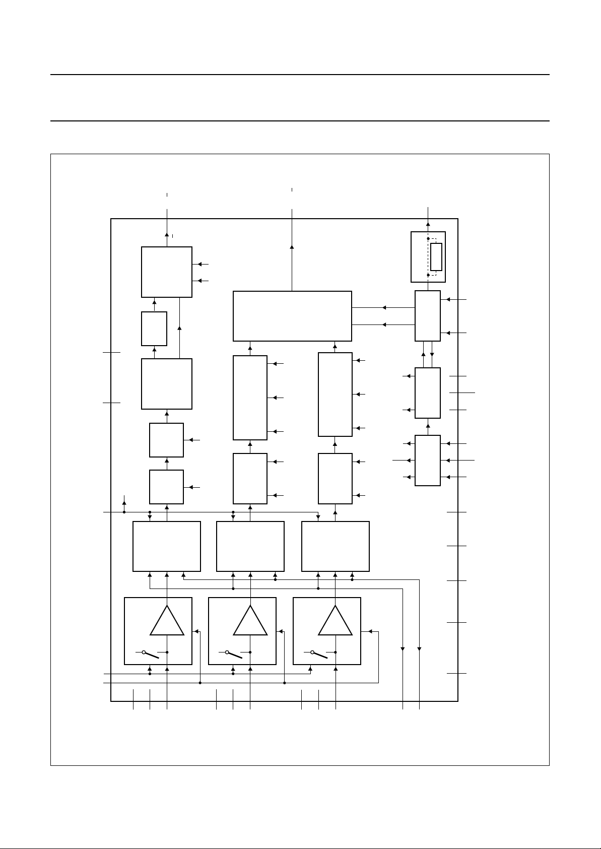
BLOCK DIAGRAM
SSD2
V
910
V
16
Y0 Y7
1 8
MIXER
DIFF
FILTER
LOW-PASS
PRE-
FILTER
DELAY
SIGN DELTA
ON/OFF
DELAY
12/14
INTERPOLATION
DOWNSAMPLING
AND
CORING
PREFILTER
UV0 UV1
11/13
U AND V
FORMATTER
ON/OFF NOTCH HOLD DELTA RESET
INTERPOLATION
DOWNSAMPLING
NOTCH HOLD DELTA RESET
AND
CORING
PREFILTER
ON/OFF
PHI
ENABLE
DELAY
ON/OFF NOTCH DELTA SIGN
WEO
MEMORY
INTERFACE
HOLD
DTO
SERIAL
INTERFACE
17
DELAY
RESET
MBE424
ref
MSCAN WEIH
MODE1
22 21 23
V50 MODE0
UPCL
41 40 42 19 18
handbook, full pagewidth
Fig.1 Block diagram.
SSD1 UPDA
V
CLAMP CLK DDD2
ref
I
CLAMP CIRCUIT
2027
39
37
SSA1
DDA1
V
V
ADC
8 BIT
x 1.5
38
INY
CLAMP CIRCUIT
34
DDA2
V
36
V
SSA2
ADC
8 BIT
x 1.5
35
INU
1996 Jan 12 3
ADC
8 BIT
x 1.5
CLAMP CIRCUIT
33
31
V
DDA3
SSA3
V
32
INV
TDA8753A
28
29
ref(L)
ref(H)
V
DEC
25 24
DDD1
V
15
SSD3
V
30
SSA4
V
26
SSA5
V
Page 4
Philips Semiconductors Product specification
YUV 8-bit analog-to-digital interface TDA8753A
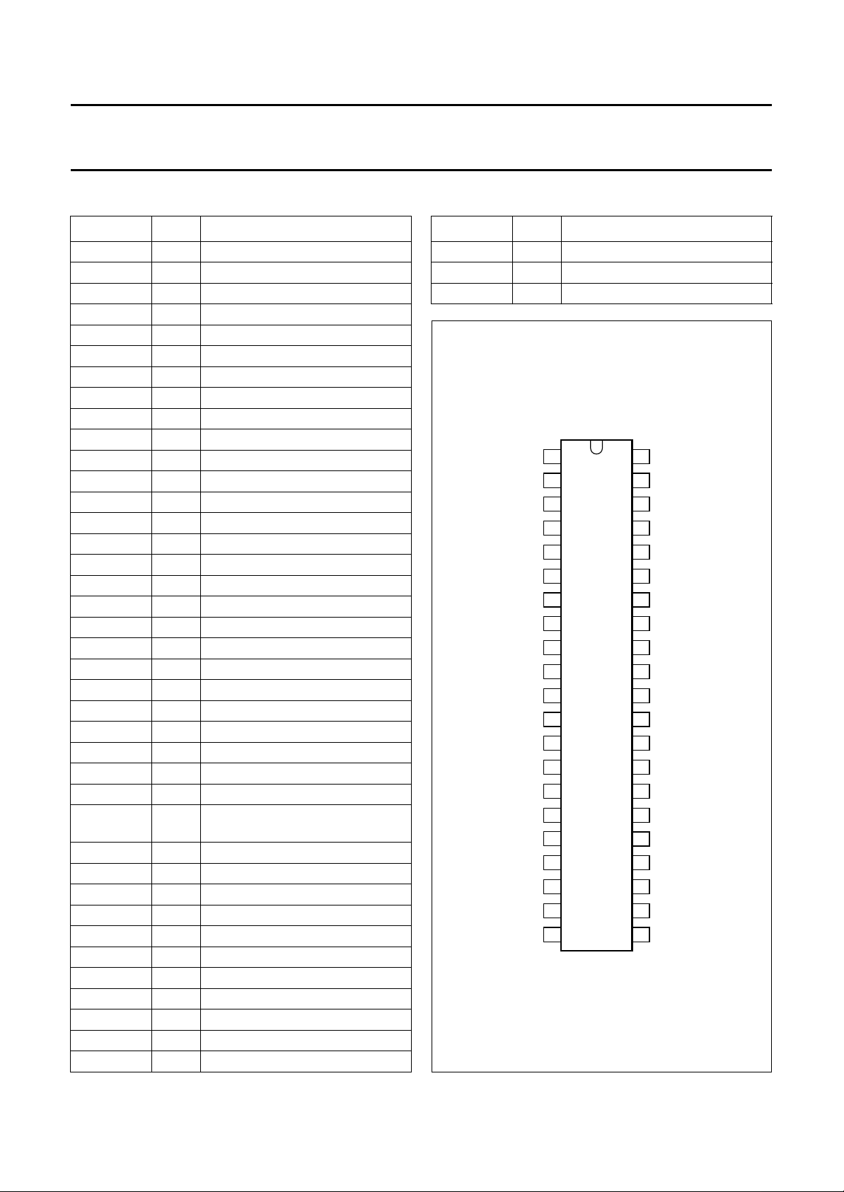
PINNING
SYMBOL PIN DESCRIPTION
Y7 1 Y data output, bit 7 (MSB)
Y6 2 Y data output, bit 6
Y5 3 Y data output, bit 5
Y4 4 Y data output, bit 4
Y3 5 Y data output, bit 3
Y2 6 Y data output, bit 2
Y1 7 Y data output, bit 1
Y0 8 Y data output, bit 0 (LSB)
V
V
DDD2
SSD2
9 digital supply voltage 2, (+5 V)
10 digital ground 2
U1 11 U data output, bit 1 (n)
U0 12 U data output, bit 0 (n − 1)
V1 13 V data output, bit 1 (n)
V0 14 V data output, bit 0 (n − 1)
V
SSD3
15 digital ground 3
CLK 16 clock input
WEO 17 write enable output
WEI 18 write enable input
H
ref
19 horizontal reference signal input
CLAMP 20 clamp control input
MODE1 21 test mode select
MODE0 22 test mode select
MSCAN 23 test pin
V
SSD1
V
DDD1
V
SSA5
I
ref
DEC
ref(L)
24 digital ground 1
25 digital supply voltage 1 (+5 V)
26 analog ground 5
27 current level reference
28 decoupling output from reference
LOW
V
V
V
ref(H)
SSA4
DDA3
29 reference voltage input (HIGH)
30 analog ground 4
31 analog supply voltage 3, (+5 V)
INV 32 V analog voltage input
V
V
SSA3
DDA2
33 analog ground 3
34 analog supply voltage 2 (+5 V)
INU 35 U analog voltage input
V
V
SSA2
DDA1
36 analog ground 2
37 analog supply voltage 1 (+5 V)
INY 38 Y analog voltage input
V
SSA1
39 analog ground 1
SYMBOL PIN DESCRIPTION
UPCL 40 control clock input
UPDA 41 serial interface data input
V50 42 data execution input
handbook, halfpage
V
CLAMP
MODE1
DDD2
V
SSD2
V
SSD3
WEO
Y7
Y6
Y5
Y4
Y3
Y2
Y1
Y0
U1
U0
V1
V0
CLK
WEI
H
ref
1
2
3
4
5
6
7
8
9
10
11
TDA8753A
12
13
14
15
16
17
18
19
20
MBE425
42
41
40
39
38
37
36
35
34
33
32
31
30
29
28
27
26
25
24
23
2221
V50
UPDA
UPCL
V
SSA1
INY
V
DDA1
V
SSA2
INU
V
DDA2
V
SSA3
INV
V
DDA3
V
SSA4
V
ref(H)
DEC
ref(L)
I
ref
V
SSA5
V
DDD1
V
SSD1
MSCAN
MODE0
Fig.2 Pin configuration.
1996 Jan 12 4
Page 5

Philips Semiconductors Product specification
YUV 8-bit analog-to-digital interface TDA8753A
FUNCTIONAL DESCRIPTION
Analog-to-digital converter
The TDA8753 implements 3 independent CMOS 8-bit
analog-to-digital converters. The converters use a
multi-step approach with offset compensated
comparators.
Clamping
An internal clamping circuit is provided in each of the
3 analog channels. The analog pins INY, INV and INU are
switched to on-chip clamping levels during an active pulse
on the clamp input CLP.The clamping level in the
Y channel is code level 16. The clamping level in the U/V
channel is code level 128 (output code 0 in the
2's complement description) see Tables 3 and 4.
Sample rate converter
A sample rate converter is integrated in the TDA8753A to
facilitate programming of the horizontal aspect ratio which
can be varied from a factor 1 to 2.
This includes conversion from 16/9 to 14/9 and 4/3. In the
U/V channel a linear interpolation is sufficient because of
the four times oversampling.
The TDA8753A has three addressable control registers
which can be loaded via the signals UPDA and UPCL.
The format of this bus is fixed according to mode 0 of the
8051 family UART at 1 Mbaud (8 bits are transmitted, LSB
first).
Serial interface protocol
P
OWER-ON STATE
When powered up the SIO is in an unknown state and all
data in the registers is random. When signals are applied
to UPCL and UPDA in this state, the behaviour is
unpredictable. The only way to exit from this state to a
known state is apply a V50 signal to the TDA8753A.
I
NITIALIZATION STATE
From power-on or any other state, the INIT state is entered
(at the latest) one TDA8753A clock period after the end of
the V50 HIGH state. In this state the F0, F1 and F2
TDA8753A registers are loaded with the values that are in
the corresponding line buffers BF0, BF1 and BF2. The first
time V50 is issued after power-on, this data is unknown.
After a rising UPCL edge has been detected, the address
reception state is entered.
Discrete time oscillator (DTO)
A discrete time oscillator is used to calculate for every
sample of the phase delay that is needed for a given
compression factor.
Serial interface (SIO)
All controls are sent to the TDA8753A via a serial
microprocessor interface. Data from this interface will be
made active at the vertical input pulse V50.
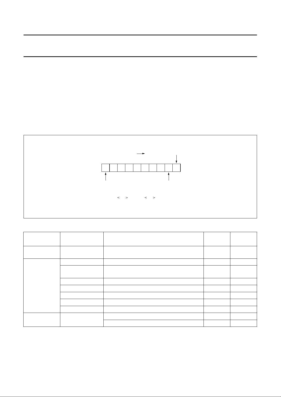
handbook, halfpage
11110010
first data bit
of data value
for address F2
register
last address
bit received
(in this example address received is F2 hex)
DDRESS RECEPTION STATE
A
Bits are counted at each rising UPCL edge. The next 8 bits
received on UPDA line are considered as address bits.
The address reception is illustrated in Fig.3.
incoming stream
first bit
received
MBE426
Fig.3 Address reception.
1996 Jan 12 5
Page 6
Philips Semiconductors Product specification
YUV 8-bit analog-to-digital interface TDA8753A
The TDA8753A registers have address F0, F1 and F2
hexadecimal notation. Whenever the received address
(decoded on the first 8 bits received) is one of these, the
event is recorded in such a way that the next data received
by the TDA8753A will be captured in the line
buffer BF0, BF1 and BF2 respectively.
When 8 bits have been received, the data reception state
is entered. The address reception state can also be exited
at any time when V50 goes HIGH. The F0, F1 and F2
registers may not be loaded properly if there is some
activity in progress on the incoming line.
handbook, halfpage
110XXXXX
first bit of next
address stream
Data value is F2 0:2 = 110(DEL 0:2 )
incoming stream
D
ATA RECEPTION STATE
The next 8 bits are considered as data bits according to
the format of Fig.4.
When 8 data bits have been received, the data is recorded
in the BF0, BF1 or BF2 line buffers if the previous address
recorded was F0 hex, F1 hex or F2 hex respectively.
The bit count is then reset to zero and the address
reception state is entered. This state may be ended any
time when V50 goes HIGH but in that condition F0, F1 and
F2 registers may not be loaded properly.
last address
bit received
first data bit of value
(e.g. for address F2 register)
MBE427
Fig.4 Data reception.
Table 1 Data allocation
ADDRESS PARAMETER FUNCTION
F0H CF compression factor value will be (1 + cf/255)
NUMBER
OF BITS
8 7:0
POSITION
which results in a range from 1 to 2
F1H UV_CORING coring definition in U and V channels; see Table 5 2 1:0
UV_FILTER_TYPE notch filter selection in U and V channels
12
(0 = 4 MHz; 1 = 2 MHz)
PRE_ON luminance prefilter active 1 3
NOTCH_ON notch prefilter active 1 4
DTO_ON DTO control 1 5
SEL_DTO_RES select DTO reset (0 = WE; 1 = H
)16
ref
WEO_DEL_SEL select delay in WEO
F2H Y_VAR_DELAY luminance delay compression (see Table 5)
not used; load 0 5 7:2
BIT
1996 Jan 12 6
Page 7

Philips Semiconductors Product specification
YUV 8-bit analog-to-digital interface TDA8753A
LIMITING VALUES
In accordance with the Absolute Maximum Rating System (IEC 134).
SYMBOL PARAMETER CONDITIONS MIN. MAX. UNIT
V
DDD
V
DDA
− V
V
DDA
V
I
V
clk(p-p)
T
stg
T
amb
DDD
THERMAL RESISTANCE
SYMBOL PARAMETER VALUE UNIT
R
th j-a
digital supply voltage −0.3 6.5 V
analog supply voltage −0.3 6.5 V
supply voltage difference −0.5 +0.5 V
input voltage referenced to AGND − V
AC input voltage for switching
referenced to DGND − V
DDA
DDD
V
V
(peak-to-peak value)
storage temperature −55 +150 °C
operating ambient temperature 0 +70 °C
thermal resistance from junction to ambient in free air 45 K/W
HANDLING
Inputs and outputs are protected against electrostatic discharge in normal handling. However, to be totally safe, it is
desirable to take normal precautions appropriate to handling integrated circuits.
CHARACTERISTICS
V
DDA=VDDD
V
ref(H)
T
= 0 to 70 °C; typical values measured at V
amb
= 4.75 to 5.25 V; V
= 2.38 V; f
and V
SSA
= 20 MHz with 50% duty cycle; 5.6 kΩ (5%) connected between I
clk
shorted together; V
SSD
DDA=VDDD
DDA
− V
= −0.1 to +0.1 V (see note 1);
DDD
= 5 V; unless otherwise specified.
ref
and V
; CL = 15 pF;
DDA
SYMBOL PARAMETER CONDITIONS MIN. TYP. MAX. UNIT
Supply
V
DDA
V
DDD
I
DDA
I
DDD
Digital inputs and clock input (WE, H
V
IL
V
IH
C
I
input leakage current VI=0V; V
IL
I
analog supply voltage 4.75 5.0 5.25 V
digital supply voltage 4.75 5.0 5.25 V
analog supply current − 55 63 mA
digital supply current − 45 55 mA
, CLAMP, MODE1, MODE0, SCCL, UPCL, UPDA and V50)
ref
LOW level input voltage 0 − 0.8 V
HIGH level input voltage 2.0 − V
DDD
V
input capacitance − 715pF
=5V −10 − +10 µA
DDD
1996 Jan 12 7
Page 8

Philips Semiconductors Product specification
YUV 8-bit analog-to-digital interface TDA8753A
SYMBOL PARAMETER CONDITIONS MIN. TYP. MAX. UNIT
Clamp and references [I
A
C
Z
CL
clamp
ADC
clamping accuracy Y −4 − +1 LSB
serial clamp capacitor 10 22 − nF
internal impedance between
pin 29 and V
V
ref(H)
converter reference HIGH, applied
ref
, DEC
SSA
ref(L)
to pin 29
V
DECref(L)
converter reference voltage LOW,
applied to pin 28
Y analog input (INY); V
V
i(p-p)
input voltage, full range
ref(H)
= 2.38 V, V
(peak-to-peak value)
I
i
C
I
input current clamp non-active − 5 100 nA
input capacitance −−15 pF
U,V analog inputs (INU and INV); V
V
I
i
C
i(p-p)
I
input voltage (peak-to-peak value) ramp input − 1.26 − V
input current clamp non-active − 5 100 nA
input capacitance −−15 pF
Inputs isolation
α
act
crosstalk between INY, INU and
INV
and V
ref(L)
ref(H)
]
ref(H)
U and V −1 − +1 LSB
V
ref(H)
= 0.39 V; see Table 4
ramp input − 1.26 − V
= 2.38 V, V
= 0.39 V; see Table 4
ref(L)
− 420 −Ω
− 2.38 − V
= 2.38 V − 0.39 − V
−−−50 dB
Digital outputs (Y0 to Y7, U1, U0, V1 and V0); see Table 3
V
OL
V
OH
Analog signal processing (f
G
diff
Φ
diff
f
all
LOW level output voltage IOL= 1.6 mA 0 − 0.5 V
HIGH level output voltage IOH= 0.4 mA 2.4 − V
= 20 MHz)
CLK
DDD
V
differential gain note 2 − 1.5 − %
differential phase note 2 − 1.0 − deg
harmonics (full scale) all
components
note 3; Y −−53 − dB
U and V −−55 − dB
SVR supply voltage ripple rejection note 4 − 2 − %/V
B bandwidth −1 dB; note 5 − 6 − MHz
Transfer function (f
= 16 MHz)
clk
INL integral non-linearity ramp input −±0.75 − LSB
DNL differential non-linearity ramp input; Y −±0.5 ±0.75 LSB
ramp input; U and V −±0.6 ±0.9 LSB
SNR signal-to-noise ratio without
harmonics
note 6; Y 41 44.5 − dB
U and V 42 46 − dB
1996 Jan 12 8
Page 9

Philips Semiconductors Product specification
YUV 8-bit analog-to-digital interface TDA8753A
SYMBOL PARAMETER CONDITIONS MIN. TYP. MAX. UNIT
Timing (f
f
clk
t
CP(H)
t
CP(L)
t
ds
t
hd
t
d
t
CLKr
t
CLKf
t
su;Href
t
hd;Href
t
r
t
f
t
CLP
= 20 MHz; CL= 15 pF); see Figs 7 and 10; note 7
clk
maximum input clock frequency 20 −−MHz
clock pulse width HIGH 22 −−ns
clock pulse width LOW 22 −−ns
sampling delay − 4 − ns
output hold time 7 −−ns
output delay time −−32 ns
clock rise time 3 5 − ns
clock fall time 3 5 − ns
HREF set-up time 7 −−ns
HREF hold time 3 −−ns
data output rise time − 10 − ns
data output fall time − 10 − ns
minimum time for active clamp
pulse width
t
su;WE
t
hd;WE
t
XLXL
t
QVXH
WE set-up time 7 −−ns
WE hold time 3 −−ns
serial port clock cycle time f
output data set-up to rising edge
of clock
t
XHQH
output data hold time after rising
edge of clock
t
W
t
VC
Sample rate converter (f
V50 pulse duration 2 −−ms
V50 to clock time 2 −−ms
= 20 MHz)
clk
ΦY Y phase accuracy f
FUV UV phase accuracy f
Y
UV
Y
UV
fr
fr
step
step
Y frequency response fiY= 0 to 5 MHz −±0.5 − dB
UV frequency response f
Y step size − 1 − ns
UV step size − 4 − ns
2.3 2.5 −µs
= 12 MHz 1 −−µs
xtal
700 −−ns
50 −−ns
= 0 to 5 MHz −±1−ns
iY
= 0 to 1.5 MHz −±4−ns
iUV
= 0 to 1.5 MHz −±0.5 − dB
iUV
1996 Jan 12 9
Page 10

Philips Semiconductors Product specification
YUV 8-bit analog-to-digital interface TDA8753A
Notes to the Characteristics
1. V
2. Measurement carried out using video amplifier type VM700A, where the video analog signal (Y channel) is
3. The input conditions are related as follows:
4. Supply voltage ripple rejection: SVR; relative variation of the full-scale range of analog input for a supply voltage
5. The −1 dB bandwidth is the frequency value for which the analog reconstructed (glitch-free) output signal is
6. The signal-to-noise ratio without harmonics is measured under a 16 MHz clock frequency. This value is given for a
7. Output data acquisition: Output data is available after the maximum delay of td.
Table 2 Mode selection
DDA
and V
should be supplied from the same power supply and decoupled separately.
DDD
reconstructed via the DAC.
Y − V
U and V − V
variation of 0.5 V. SVR = [∆ (V
= 1.26 V, fi= 4.43 MHz
i(p-p)
= 1.26 V, fi= 1.5 MHz.
i(p-p)
I(0)
− V
I(255)
]/[V
I(o)
− V
I(255)
]/∆V
DDA
.
compressed in term of number of codes, by −1 dB (respectively for −3 dB bandwidth).
4.43 MHz input frequency on the Y channel (1.5 MHz on the U and V channels).
MODE1 MODE0 MODE
0 0 normal configuration
Table 3 Output data coding
OUTPUT PORT BIT OUTPUT DATA
YY7Y
Y6 Y
Y5 Y
Y4 Y
Y3 Y
Y2 Y
Y1 Y
Y0 Y
UU1
U0 U
VV1
V0 V
7Y
0
6Y
0
5Y
0
4Y
0
3Y
0
2Y
0
1Y
0
0Y
0
U
7U
0
6U
0
V
7V
0
6V
0
7Y
1
6Y
1
5Y
1
4Y
1
3Y
1
2Y
1
1Y
1
0Y
1
5U
0
4U
0
5V
0
4V
0
7Y
2
6Y
2
5Y
2
4Y
2
3Y
2
2Y
2
1Y
2
0Y
2
3U
0
2U
0
3V
0
2V
0
7
3
6
3
5
3
4
3
3
3
2
3
1
3
0
3
1
0
0
0
1
0
0
0
1996 Jan 12 10
Page 11

Philips Semiconductors Product specification
YUV 8-bit analog-to-digital interface TDA8753A
Table 4 Internal ADC data coding as a function of the analog input
STEP INPUT VOLTAGE INTERNAL BINARY OUTPUTS REMARKS
Underflow <0.26 00000000
0 0.26 00000000 V
1 - 00000001
.... .... ........
16 0.34 00010000 clamp level of Y channel
.... .... ........
128 0.89 10000000 clamp level of U and V channels
.... .... ........
254 − 11111110
255 1.52 11111111 V
Overflow >1.52 11111111
Table 5 Coring and luminance delay
DECref(L)
ref(H)
/1.5
− 0.1 V/1.5
UV_CORING INTERNAL CORING CORRECTION
F1:1 F1:0 F2:1 F2:0
0 0 coring off 0 0 0
0 1 +1/−101 1
1 0 +1/−010 2
1 1 +2/−111 3
IN U AND V CHANNELS
(AROUND CODE 128 LEVEL)
Y_V AR_DELAY INTERNAL DELA Y FOR Y P ATH
AT PREFILTER INPUT
(CLOCK PULSE)
1996 Jan 12 11
Page 12

Philips Semiconductors Product specification
YUV 8-bit analog-to-digital interface TDA8753A
t
CPH
CPL
27 mm
1/1 page = 296 mm (Datasheet)
t
The value D is equal to 15.
TIMING
CLK
V
l
DATA
D0 - D7
sample N
DATA
N-D
1.4 V
sample N + 1
t
dS
DATA
N-D+1
t
d
sample N + 2
t
HD
DATA
N-D+2
DATA
N-D+2
2.4 V
1.4 V
0.4 V
MSB269
Fig.5 Timing diagram.
handbook, full pagewidth
digital
output
level
255
Y : 16
U,V : 128
black-level
0
CLP
Fig.6 Clamp control timing.
1996 Jan 12 12
clamping
t
MSA645
time
CLP
Page 13

Philips Semiconductors Product specification
YUV 8-bit analog-to-digital interface TDA8753A
handbook, full pagewidth
CLK
WE
data
123 15
t
su
output data valid
t
hd
MBE430
The output data is valid 15 clock periods after WE goes HIGH.
Fig.7 Set-up and hold time definition; WE signal.
handbook, full pagewidth
CLK
WE
t
su
data
K x 15 x periods
output data valid
MBE431
When the WE period is a whole multiple of 15 clock periods, the output data is valid without any clock delay.
The internal circuit always gives an internal 15 clock period as illustrated in Fig.7.
Fig.8 Timing diagram; WE signal.
1996 Jan 12 13
Page 14

Philips Semiconductors Product specification
YUV 8-bit analog-to-digital interface TDA8753A
t
handbook, full pagewidth
V50
UPCL
d
t
XLXL
t
XHQX
handbook, full pagewidth
t
QVXH
Fig.9 Timing of the asynchronous interface.
CLK
t
hd
WEO
YUV
outputs
MBE432
MBE428
Fig.10 Outputs hold time.
1996 Jan 12 14
Page 15

Philips Semiconductors Product specification
YUV 8-bit analog-to-digital interface TDA8753A
handbook, full pagewidth
Fig.11 Digital inputs WE and H
INTERNAL PIN CONFIGURATION
handbook, full pagewidth
DIGITAL INPUTS
16,
18 to 23,
40 to 42
V
DDD
CLK
t
su;X
t
hd;X
; set-up and hold time.
REF
DIGITAL OUTPUTS
1 to 8,
11 to 14,
17
MBE429
V
DDD
V
SSD
ANALOG INPUTS
27
29
30
V
SSA
V
SSA
Fig.12 Internal pin configuration.
1996 Jan 12 15
32, 35, 38
V
SSD
V
V
I
DDA
SSA
I
I
MBE419
Page 16

Philips Semiconductors Product specification
YUV 8-bit analog-to-digital interface TDA8753A
APPLICATION INFORMATION
5 V
5 V
5.6 µH
100 nF
4.7 µF
1
2
3
4
5
6
7
8
9
10
11
12
13
14
15
16
17
18
19
20
21
TDA8753A
42
41
40
39
22 nF
38
37
36
35
34
33
32
31
30
29
22 nF
28
27
26
22 nF
25
24
23
22
Y
22 nF
U
22 nF
V
5.6 kΩ
100
nF
4.7 µF
100 nF
220
µF
220 Ω
220 Ω
5.6 µH
5 V
220 uF
MBE433
Analog and digital supplies should be separated and decoupled. Test pins MODE1, MODE0 and MSCAN must be connected to digital ground.
Fig.13 Application diagram.
1996 Jan 12 16
Page 17

Philips Semiconductors Product specification
YUV 8-bit analog-to-digital interface TDA8753A
PACKAGE OUTLINE
SDIP42: plastic shrink dual in-line package; 42 leads (600 mil)
D
seating plane
L
Z
42
pin 1 index
e
b
SOT270-1
M
E
A
2
A
A
1
w M
b
1
22
E
c
(e )
M
1
H
1
0 5 10 mm
scale
DIMENSIONS (mm are the original dimensions)
A
A
A
UNIT b
mm
Note
1. Plastic or metal protrusions of 0.25 mm maximum per side are not included.
max.
5.08 0.51 4.0
OUTLINE
VERSION
SOT270-1
12
min.
max.
IEC JEDEC EIAJ
1.3
0.8
b
1
0.53
0.40
REFERENCES
0.32
0.23
cEe M
(1) (1)
D
38.9
38.4
1996 Jan 12 17
14.0
13.7
21
(1)
Z
1
L
M
E
3.2
15.80
2.9
15.24
EUROPEAN
PROJECTION
17.15
15.90
e
w
H
0.181.778 15.24
ISSUE DATE
90-02-13
95-02-04
max.
1.73
Page 18

Philips Semiconductors Product specification
YUV 8-bit analog-to-digital interface TDA8753A
SOLDERING
Introduction
There is no soldering method that is ideal for all IC
packages. Wave soldering is often preferred when
through-hole and surface mounted components are mixed
on one printed-circuit board. However, wave soldering is
not always suitable for surface mounted ICs, or for
printed-circuits with high population densities. In these
situations reflow soldering is often used.
This text gives a very brief insight to a complex technology.
A more in-depth account of soldering ICs can be found in
our
“IC Package Databook”
Soldering by dipping or by wave
The maximum permissible temperature of the solder is
260 °C; solder at this temperature must not be in contact
with the joint for more than 5 seconds. The total contact
time of successive solder waves must not exceed
5 seconds.
DEFINITIONS
Data sheet status
Objective specification This data sheet contains target or goal specifications for product development.
Preliminary specification This data sheet contains preliminary data; supplementary data may be published later.
Product specification This data sheet contains final product specifications.
(order code 9398 652 90011).
The device may be mounted up to the seating plane, but
the temperature of the plastic body must not exceed the
specified maximum storage temperature (T
printed-circuit board has been pre-heated, forced cooling
may be necessary immediately after soldering to keep the
temperature within the permissible limit.
Repairing soldered joints
Apply a low voltage soldering iron (less than 24 V) to the
lead(s) of the package, below the seating plane or not
more than 2 mm above it. If the temperature of the
soldering iron bit is less than 300 °C it may remain in
contact for up to 10 seconds. If the bit temperature is
between 300 and 400 °C, contact may be up to 5 seconds.
stg max
). If the
Limiting values
Limiting values given are in accordance with the Absolute Maximum Rating System (IEC 134). Stress above one or
more of the limiting values may cause permanent damage to the device. These are stress ratings only and operation
of the device at these or at any other conditions above those given in the Characteristics sections of the specification
is not implied. Exposure to limiting values for extended periods may affect device reliability.
Application information
Where application information is given, it is advisory and does not form part of the specification.
LIFE SUPPORT APPLICATIONS
These products are not designed for use in life support appliances, devices, or systems where malfunction of these
products can reasonably be expected to result in personal injury. Philips customers using or selling these products for
use in such applications do so at their own risk and agree to fully indemnify Philips for any damages resulting from such
improper use or sale.
1996 Jan 12 18
Page 19

Philips Semiconductors Product specification
YUV 8-bit analog-to-digital interface TDA8753A
NOTES
1996 Jan 12 19
Page 20

Philips Semiconductors – a worldwide company
Argentina: IEROD, Av. Juramento 1992 - 14.b, (1428)
BUENOS AIRES, Tel. (541)786 7633, Fax. (541)786 9367
Australia: 34 Waterloo Road, NORTH RYDE, NSW 2113,
Tel. (02)805 4455, Fax. (02)805 4466
Austria: Triester Str. 64, A-1101 WIEN, P.O. Box 213,
Tel. (01)60 101-1236, Fax. (01)60 101-1211
Belgium: Postbus 90050, 5600 PB EINDHOVEN, The Netherlands,
Tel. (31)40-2783749, Fax. (31)40-2788399
Brazil: Rua do Rocio 220 - 5
CEP: 04552-903-SÃO PAULO-SP, Brazil,
P.O. Box 7383 (01064-970),
Tel. (011)821-2333, Fax. (011)829-1849
Canada: PHILIPS SEMICONDUCTORS/COMPONENTS:
Tel. (800) 234-7381, Fax. (708) 296-8556
Chile: Av. Santa Maria 0760, SANTIAGO,
Tel. (02)773 816, Fax. (02)777 6730
China/Hong Kong: 501 Hong Kong Industrial Technology Centre,
72 Tat Chee Avenue, Kowloon Tong, HONG KONG,
Tel. (852)2319 7888, Fax. (852)2319 7700
Colombia: IPRELENSO LTDA, Carrera 21 No. 56-17,
77621 BOGOTA, Tel. (571)249 7624/(571)217 4609,
Fax. (571)217 4549
Denmark: Prags Boulevard 80, PB 1919, DK-2300
COPENHAGEN S, Tel. (45)32 88 26 36, Fax. (45)31 57 19 49
Finland: Sinikalliontie 3, FIN-02630 ESPOO,
Tel. (358)0-615 800, Fax. (358)0-61580 920
France: 4 Rue du Port-aux-Vins, BP317,
92156 SURESNES Cedex,
Tel. (01)4099 6161, Fax. (01)4099 6427
Germany: P.O. Box 10 51 40, 20035 HAMBURG,
Tel. (040)23 53 60, Fax. (040)23 53 63 00
Greece: No. 15, 25th March Street, GR 17778 TAVROS,
Tel. (01)4894 339/4894 911, Fax. (01)4814 240
India: Philips INDIA Ltd, Shivsagar Estate, A Block,
Dr. Annie Besant Rd. Worli, Bombay 400 018
Tel. (022)4938 541, Fax. (022)4938 722
Indonesia: Philips House, Jalan H.R. Rasuna Said Kav. 3-4,
P.O. Box 4252, JAKARTA 12950,
Tel. (021)5201 122, Fax. (021)5205 189
Ireland: Newstead, Clonskeagh, DUBLIN 14,
Tel. (01)7640 000, Fax. (01)7640 200
Italy: PHILIPS SEMICONDUCTORS S.r.l.,
Piazza IV Novembre 3, 20124 MILANO,
Tel. (0039)2 6752 2531, Fax. (0039)2 6752 2557
Japan: Philips Bldg13-37, Kohnan 2-chome, Minato-ku, TOKYO 108,
Tel. (03)3740 5130, Fax. (03)3740 5077
Korea: Philips House, 260-199 Itaewon-dong,
Yongsan-ku, SEOUL, Tel. (02)709-1412, Fax. (02)709-1415
Malaysia: No. 76 Jalan Universiti, 46200 PETALING JAYA,
SELANGOR, Tel. (03)750 5214, Fax. (03)757 4880
Mexico: 5900 Gateway East, Suite 200, EL PASO, TX 79905,
Tel. 9-5(800)234-7381, Fax. (708)296-8556
th
floor, Suite 51,
Netherlands: Postbus 90050, 5600 PB EINDHOVEN, Bldg. VB,
Tel. (040)2783749, Fax. (040)2788399
New Zealand: 2 Wagener Place, C.P.O. Box 1041, AUCKLAND,
Tel. (09)849-4160, Fax. (09)849-7811
Norway: Box 1, Manglerud 0612, OSLO,
Tel. (022)74 8000, Fax. (022)74 8341
Pakistan: Philips Electrical Industries of Pakistan Ltd.,
Exchange Bldg. ST-2/A, Block 9, KDA Scheme 5, Clifton,
KARACHI 75600, Tel. (021)587 4641-49,
Fax. (021)577035/5874546
Philippines: PHILIPS SEMICONDUCTORS PHILIPPINES Inc.,
106 Valero St. Salcedo Village, P.O. Box 2108 MCC, MAKATI,
Metro MANILA, Tel. (63) 2 816 6380, Fax. (63) 2 817 3474
Portugal: PHILIPS PORTUGUESA, S.A.,
Rua dr. António Loureiro Borges 5, Arquiparque - Miraflores,
Apartado 300, 2795 LINDA-A-VELHA,
Tel. (01)4163160/4163333, Fax. (01)4163174/4163366
Singapore: Lorong 1, Toa Payoh, SINGAPORE 1231,
Tel. (65)350 2000, Fax. (65)251 6500
South Africa: S.A. PHILIPS Pty Ltd.,
195-215 Main Road Martindale, 2092 JOHANNESBURG,
P.O. Box 7430, Johannesburg 2000,
Tel. (011)470-5911, Fax. (011)470-5494
Spain: Balmes 22, 08007 BARCELONA,
Tel. (03)301 6312, Fax. (03)301 42 43
Sweden: Kottbygatan 7, Akalla. S-164 85 STOCKHOLM,
Tel. (0)8-632 2000, Fax. (0)8-632 2745
Switzerland: Allmendstrasse 140, CH-8027 ZÜRICH,
Tel. (01)488 2211, Fax. (01)481 77 30
Taiwan: PHILIPS TAIWAN Ltd., 23-30F, 66, Chung Hsiao West
Road, Sec. 1. Taipeh, Taiwan ROC, P.O. Box 22978,
TAIPEI 100, Tel. (886) 2 382 4443, Fax. (886) 2 382 4444
Thailand: PHILIPS ELECTRONICS (THAILAND) Ltd.,
209/2 Sanpavuth-Bangna Road Prakanong,
Bangkok 10260, THAILAND,
Tel. (66) 2 745-4090, Fax. (66) 2 398-0793
Turkey:Talatpasa Cad. No. 5, 80640 GÜLTEPE/ISTANBUL,
Tel. (0212)279 27 70, Fax. (0212)282 67 07
Ukraine: Philips UKRAINE, 2A Akademika Koroleva str., Office 165,
252148 KIEV, Tel.380-44-4760297, Fax. 380-44-4766991
United Kingdom: Philips Semiconductors LTD.,
276 Bath Road, Hayes, MIDDLESEX UB3 5BX,
Tel. (0181)730-5000, Fax. (0181)754-8421
United States:811 East Arques Avenue, SUNNYVALE,
CA 94088-3409, Tel. (800)234-7381, Fax. (708)296-8556
Uruguay: Coronel Mora 433, MONTEVIDEO,
Tel. (02)70-4044, Fax. (02)92 0601
Internet: http://www.semiconductors.philips.com/ps/
For all other countries apply to: Philips Semiconductors,
International Marketing and Sales, Building BE-p,
P.O. Box 218, 5600 MD EINDHOVEN, The Netherlands,
Telex 35000 phtcnl, Fax. +31-40-2724825
SCDS47 © Philips Electronics N.V. 1996
All rights are reserved. Reproduction in whole or in part is prohibited without the
prior written consent of the copyright owner.
The information presented in this document does not form part of any quotation
or contract, is believed to be accurate and reliable and may be changed without
notice. No liability will be accepted by the publisher for any consequence of its
use. Publication thereof does not convey nor imply any license under patent- or
other industrial or intellectual property rights.
Printed in The Netherlands
537021/1100/02/pp20 Date of release: 1996 Jan 12
Document order number: 9397 750 00564
 Loading...