

Page 1

DATA SH EET
Preliminary specification
Supersedes data of 1995 Mar 08
File under Integrated Circuits, IC02
1996 Mar 11
INTEGRATED CIRCUITS
TDA8745
Satellite sound receiver with
I
2
C-bus control
Page 2

1996 Mar 11 2
Philips Semiconductors Preliminary specification
Satellite sound receiver with I2C-bus control
TDA8745
FEATURES
• On-chip frequency synthesizer and mixer:
– tuning range 4 to 9.77 MHz
– reference oscillator 4 MHz (using a crystal or 4 MHz
frequency source)
• IF input switches allowing selection of various IF
bandwidths (wide or narrow)
• Demodulation of two audio signals by wide band
Phase-Locked Loops (PLLs)
• Audio level control after PLL (modulation depth setting)
• Noise Reduction (NR) bypass for use with main audio
signals
• Left, right and mono output [1⁄2(l + r)] on SCART level
• External audio inputs (for decoder connection)
• Selectable de-emphasis (DEEM) 50 µs, 75 µs, J17 and
flat response
• I2C-bus control of all functions
• Two selectable addresses
• Carrier presence detector with automatic mute option.
APPLICATIONS
• Satellite receivers
• TV sets
• Video recorders.
GENERAL DESCRIPTION
The TDA8745 is the successor of the TDA8740 and
TDA8741. The device contains the functionality of the
TDA8740 and TDA8741 together with a synthesizer, mixer
and I
2
C-bus control.
The pin numbers mentioned in this publication refer to the
SDIP42 package; unless otherwise indicated.
ORDERING INFORMATION
TYPE
NUMBER
PACKAGE
NAME DESCRIPTION VERSION
TDA8745 SDIP42
plastic shrink dual in-line package; 42 leads (600 mil)
SOT270-1
TDA8745H QFP44
plastic quad flat package; 44 leads (lead length 1.3 mm);
body 10 × 10 × 1.75 mm
SOT307-2
Page 3

1996 Mar 11 3
Philips Semiconductors Preliminary specification
Satellite sound receiver with I2C-bus control
TDA8745
QUICK REFERENCE DATA
SYMBOL PARAMETER CONDITIONS MIN. TYP. MAX. UNIT
V
P1
synthesizer and mixer supply voltage 4.5 5.0 5.5 V
V
P2
I2C-bus supply voltage 4.5 5.0 5.5 V
V
P3
general supply voltage 8.0 12.0 13.2 V
I
P1
synthesizer and mixer supply current − 37 48 mA
I
P2
I2C-bus supply current − 0.6 − mA
I
P3
general supply current − 35 46 mA
S/N(A) signal-to-noise ratio secondary channel A-weighted;
NR = on; DEEM = 75 µs
68 77 − dB
V
i(rms)
input sensitivity (RMS value) baseband input
to mixer
S/N(A) = 40 dB;
NR = on; DEEM = 75 µs
− 0.5 1.5 mV
V
i(rms)
baseband input voltage (RMS value) THD ≤ 0.5% 200 mV
V
o
output voltage −8 −6 −4 dBV
P
tot
total power dissipation − 610 800 mW
T
stg
storage temperature −65 − +150 °C
T
amb
operating ambient temperature −20 − +70 °C
Page 4
1996 Mar 11 4
Philips Semiconductors Preliminary specification
Satellite sound receiver with I2C-bus control
TDA8745
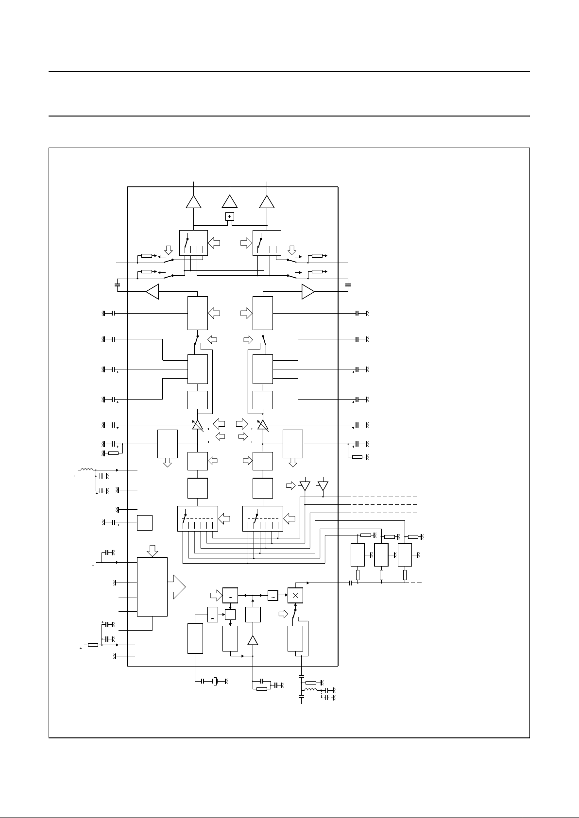
BLOCK DIAGRAM
handbook, full pagewidth
ϕ
MBE037
330 Ω
330 Ω
330
Ω
330 Ω
330 Ω
1 kΩ
470
kΩ
1
µF
HF
LIMITER
PLL
HF
LIMITER
PLL
IL2 to IL0
IR2 to IR0
PRESENCE
DETECTOR
AUDIO
LPF
NOISE
REDUCTION
OMR
12 to 3dB
LEV3 to LEV0
OML
PRESENCE
DETECTOR
BB
DC
DC
PDR
IL2
IR2
PRES DET R
C
DC R
RECT
R
C
NR D R
C
D R
DEEM OUT LDEEM OUT R
C
ATT/REC R
PDL
9
PE
11 13 15 7 8
10.7
NARROW
5
330
Ω
10 nF
10
µF
DE-EMPHASIS
50 µs
J17
10
µF
1
µF
4.7
nF
10
nF
75 µs
220 nF
AUDIO
LPF
NOISE
REDUCTION
DE-EMPHASIS
50
flat
flat µs
J17
75 µs
DEM1 and DEM0 OS1 and OS0NR
OML
OMR
O
L
O
M
O
R
23
21
22
29
30 31
24
27
26 2839 1
35 34 33 2537 38 36
EXT
L
C
D L
C
CL L
C
CL L
C
NR D L
C
DC L
V
ref
V
P3
V
P2
V
P1 AFGNDHFGND
PRES DET L
C
ATT/REC L
RECT
L
EXT
470
kΩ
1
µF
12 to 3dB
10
µF
4241
10
µF
1
µF
4.7
nF
10
nF
220 nF
203210
2.2
µF
19
V
ref
1614171812
2
PDL
PDR
I C
INTERFACE
2
VCO
frequency
synthesizer
30 to 40 MHz
N
2
CHARGE
PUMP
200
CRYSTAL
OSCILLATOR
PRE-BPF
4 MHz
MIXER
BPFN
TUN9 to TUN0
SDA
5 V
SCL
ADD
sel
I CGND
46
SYNGND
XTAL
2
40
BASEBAND
IN
IF OUT
6.8
kΩ
33
nF
3
27 pF
27 pF
27 pF
15 pF
1 µF
1000 µF
10
pF
4 MHz
10.52
NARROW
10.7
WIDE
SLF
IN-1
IN-2
IN-3
IN-4
IN-5
IN-6
R
TDA8745
(2)
(1)
(2)
(2)
47 µH
100 µH
4.7 Ω
22
nF
12 V
100 µF
22
nF
5 V
22
nF
Fig.1 Block diagram (SDIP42).
When driving more than three filters in parallel, pin 5 should be buffered.
(1) Add 15 pF for NTSC.
(2) Ceramic filters:
SFE10.7MJA10-A (narrow)
SFE10.52MJA10-A (narrow)
SFE10.7MS2-A (wide).
Page 5

1996 Mar 11 5
Philips Semiconductors Preliminary specification
Satellite sound receiver with I2C-bus control
TDA8745
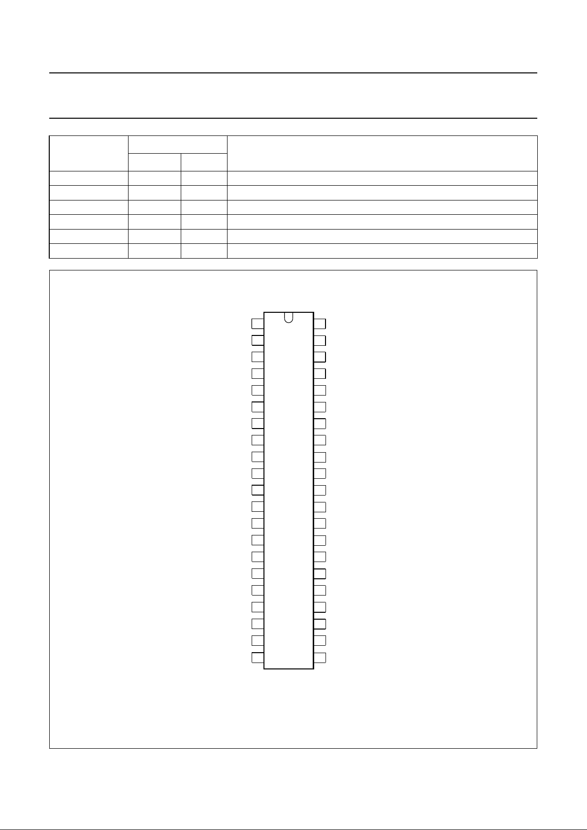
PINNING
SYMBOL
PIN
DESCRIPTION
SDIP42 QFP44
C
DC R
1 39 DC decoupling capacitor (right channel)
SLF 2 41 synthesizer loop-filter
BASEBAND IN 3 42 baseband input to mixer
V
P1
4 43 synthesizer and mixer supply voltage (+5 V)
IF OUT 5 44 intercarrier output from mixer
SYNGND 6 1 synthesizer and mixer ground
IN-5 7 2 intercarrier input 5/port expansion output 1
IN-6 8 3 intercarrier input 6/port expansion output 2
IN-1 9 4 Intercarrier input 1
HFGND 10 5 HF ground
IN-2 11 6 intercarrier input 2
ADD
sel
12 7 I2C-bus address selection
IN-3 13 8 Intercarrier input 3
I
2
CGND 14 9 I2C-bus ground
IN-4 15 10 intercarrier input 4
V
P2
16 11 I2C-bus supply voltage (+5 V)
SCL 17 12 I
2
C-bus serial clock input
SDA 18 13 I
2
C-bus serial data input/output
V
ref
19 14 decoupling capacitor for reference voltage
V
P3
20 15 general supply voltage (+12 V)
O
M
21 17 mono channel output [1⁄2(l + r)]
O
R
22 18 right channel output
O
L
23 19 left channel output
EXT
R
24 20 external audio input (right channel)
EXT
L
25 21 external audio input (left channel)
C
ATT/RECR
26 22 attack/recovery capacitor (right channel)
RECT
R
27 23 rectifier DC decoupling (right channel)
C
NR D R
28 24 noise reduction de-emphasis capacitor (right channel)
C
DR
29 25 de-emphasis capacitor (right channel)
DEEM OUT R 30 26 de-emphasis output (right channel)
C
CL R
31 27 audio pass-through input (right channel)
AFGND 32 28 AF ground
C
CL L
33 29 audio pass-through input (left channel)
DEEM OUT L 34 30 de-emphasis output (left channel)
C
DL
35 31 de-emphasis capacitor (left channel)
C
NR D L
36 32 noise reduction de-emphasis capacitor (left channel)
RECT
L
37 33 rectifier DC decoupling (left channel)
C
ATT/RECL
38 34 attack/recovery capacitor (left channel)
Page 6
1996 Mar 11 6
Philips Semiconductors Preliminary specification
Satellite sound receiver with I2C-bus control
TDA8745
PRES DET R 39 35 presence detector timing (right channel)
XTAL 40 36 crystal input for 4 MHz oscillator
PRES DET L 41 37 presence detector timing (left channel)
C
DC L
42 38 DC decoupling capacitor (left channel)
n.c. − 16 not connected
n.c. − 40 not connected
SYMBOL
PIN
DESCRIPTION
SDIP42 QFP44
handbook, halfpage
1
2
3
4
5
6
7
8
9
10
11
12
13
40
39
38
37
36
35
34
33
32
31
30
29
28
27
14
15
16
17
18
19
20
22
23
24
25
26
21
42
41
O
O
EXT
EXT
ATT/REC R
DEEM OUT R
AFGND
RECT
PRES DET R
XTAL
DC L
DC R
ATT/REC L
PRES DET LSLF
BASEBAND IN
IF OUT
SYNGND
IN-5
IN-6
IN-1
HFGND
IN-2
ADD
IN-3
I CGND
IN-4
SCL
SDA
V
P3
V
P2
V
P1
V
M
O
DEEM OUT L
RECT
TDA8745
2
ref
MBE035
C
C
L
C
NR D L
C
D L
C
CL L
C
CL R
C
D R
C
C
NR D R
R
L
R
L
R
sel
C
Fig.2 Pin configuration (SDIP42).
Page 7
1996 Mar 11 7
Philips Semiconductors Preliminary specification
Satellite sound receiver with I2C-bus control
TDA8745
Fig.3 Pin configuration (QFP44).
handbook, full pagewidth
1
2
3
4
5
6
7
8
9
10
11
33
32
31
30
29
28
27
26
25
24
23
12
13
14
15
16
17
18
19
20
21
22
44
43
42
41
40
39
38
37
36
35
34
RECT
NR D L
DEEM OUT L
AFGND
DEEM OUT R
C
C
RECT
IF OUTVBASEBAND IN
SLF
n.c.
DC L
C
DC R
P1
C
XTAL
PRES DET R
PRES DET L
ATT/REC L
C
TDA8745H
SYNGND
IN-5
IN-6
IN-1
HFGND
IN-2
ADD
IN-3
IN-4
V
2
I CGND
SCL
SDA
V
O
M
O
R
O
R
C
L
n.c.
EXTLEXT
ATT/REC R
ref
V
P3
MBE034
L
C
CL L
C
CL R
D R
R
NR D R
C
D L
C
sel
P2
Page 8

1996 Mar 11 8
Philips Semiconductors Preliminary specification
Satellite sound receiver with I2C-bus control
TDA8745
FUNCTIONAL DESCRIPTION
Satellite sound
The baseband signal coming from a satellite tuner
comprises the demodulated video signal plus a number of
sound carriers in the event of reception of a PAL, NTSC or
SECAM satellite signal.
Nearest to the video signal is the main sound carrier which
carries the mono sound related to the video. This is an FM
modulated carrier with a fixed pre-emphasis. The carrier
frequency can be in the range of 5.8 to 6.8 MHz.
Additionally, a number of optional secondary sound
carriers may be present. These can be used for stereo or
multi-language sound related to the video signal, or for
unrelated radio sound. These carriers are also FM
modulated, and for better sound quality (improved
signal-to-noise performance) broadcast satellites
(e.g. ‘ASTRA’) use a noise reduction system (adaptive
pre-emphasis circuit, combined with a fixed
pre-emphasis). These secondary carrier frequencies can
be in the range of 6.30 to 8.28 MHz.
For accurate tuning to the many sound carriers, an internal
frequency synthesizer and mixer are used to transfer the
sound carriers to intermediate frequencies of
10.7 and 10.52 MHz.
The TDA8745 contains all circuitry for the processing of
the main channel and secondary channels, from baseband
signal to line (SCART) output drivers. By means of
external band-pass filters the desired frequencies coming
from the synthesizer/mixer are routed to the IF
limiter/demodulator inputs.
Band-pass filter and mixer
Before the incoming baseband signal is applied to the
mixer, the signal is filtered. Related to the sound carriers,
the level of the video part of the baseband signal can be
much higher, so to avoid overload it is desirable to
attenuate the latter, this is also to avoid interference
(additional unwanted mix of signals after mixing).
The internal band-pass filter (pass band from
approximately 4 to 10 MHz) is completed by a simple
external notch filter. The external filter provides substantial
attenuation of the video colour carrier. The notch filter is
chosen to be external because the required notch
frequency is TV standard dependent and also because an
accurate on-chip notch filter requires a tuning mechanism
(consuming additional chip area).
The mixer is a double-balanced mixer with degeneration,
this to accommodate the level of the filter output signal.
The mixer transfers the different sound carrier frequencies
to fixed intermediate frequencies of 10.7 and 10.52 MHz.
These frequencies are fed via an internal buffer stage to
external ceramic band-pass filters before they are routed
to the two demodulator inputs. The buffer stage can drive
up to three external ceramic band-pass filters (assuming
330 Ω filter terminations) but this can be increased to four
or more by adding an external buffer.
Synthesizer
The synthesizer consists of the following parts:
• Reference oscillator
• Reference divider
• A 10-bit programmable divider
• Phase detector
• Charge pump
• Voltage Controlled Oscillator (VCO)
• Divide-by-two circuit.
The reference frequency circuit consists of a 4 MHz crystal
oscillator and a divider (by 200). The resulting reference
frequency of 20 kHz is fed to the phase detector.
The programmable divider consists of a series of cells
(divide by 2 or 3) connected as a ripple counter.
The minimum division ratio is 2
n
and the maximum division
ratio is 2
n+1
−1.
The programmable divider output signal is also fed to the
phase detector. The charge pump provides output current
pulses in accordance with the signals from the phase
detector. The final tuning voltage for the VCO is provided
by the loop filter and a buffer amplifier.
The oscillator frequency range is from
29.04 to 40.94 MHz, depending on the setting of the
programmable divider (by the TUN signal). The tuning
voltage is clipped to limit the VCO frequency range.
The frequency of the oscillator is divided-by-two before it
is applied to the mixer (to obtain the desired 10 kHz
resolution).
Left and right channel inputs
A maximum of six inputs are available (pins 9, 11, 13, 15,
7 and 8). External ceramic band-pass filters, which are
tuned to the desired intermediate frequencies, route the
signals to the inputs.
For stereo purposes the TDA8745 contains two identical
secondary sound processing channels (secondary
channel 1 will also be referred to as ‘left’ or ‘language 1’
and secondary channel 2 as ‘right’ or ‘language 2’).
Page 9

1996 Mar 11 9
Philips Semiconductors Preliminary specification
Satellite sound receiver with I2C-bus control
TDA8745
With the input selection every input pin of the left and/or
right channel can be independently selected. Input
selection for the left channel is controlled by the IL signal
and for the right channel by the IR signal.
From the inputs, the signals are coupled to the
limiter/amplifier and to the PLL demodulator of each
channel. The output signal from the PLL is routed to both
the presence detector and audio level control.
The inputs of pins 7 and 8 can be changed into digital
outputs for external switching purposes, set by the so
called Port Extension bit (PE). Not used inputs should be
connected to ground. Note that the inputs of pins 7 and 8
are also floating when not in Port Extension mode.
Presence detector
The presence detector is used to determine if a carrier is
present on the channel of interest. It does so by measuring
the amount of high frequency noise (>20 kHz) in the audio
signal, which is directly related to the C/N (carrier-to-noise
ratio) at the IF input. If a carrier is present, these high
frequencies are fairly moderate, if no carrier is present,
strong noise components are present.
The audio signal, first high-pass filtered and then rectified,
is filtered by the components at pins 41 and 39
(PRES DET L and PRES DET R). The DC level at this pin
is then compared with an internal reference voltage. If the
level at pins 41 and 39 exceeds this voltage level, the
presence detector output goes HIGH (no carrier).
This output signal can be used to drive the output mute (if
bit PDM = 1; see Section “Output selection”) and can be
monitored by reading bits PDL and PDR. The detection
level can be modified by changing the leakage resistor at
pins 41 and 39, a higher resistor value gives a ‘no carrier’
response ant C/N levels detected as ‘carrier present’ with
a lower resistor value.
Audio level control
Each demodulator output signal is amplified in a buffer
amplifier and DC decoupled by means of electrolytic
capacitors connected to pin 42 (left) and pin 1 (right).
The output level of all channels is −6 dBV typical at a
frequency deviation of the FM signal of 54% of the
maximum deviation (i.e 0.54 × 85 kHz = 46 kHz for the
main channel and 0.54 × 50 kHz = 27 kHz for the
secondary channels) at 1 kHz modulation frequency
(reference level).
To adjust for different (main channel) modulation depths
used at some satellites the audio level is made adjustable,
the signal can be controlled in steps of 1 dB from
−12 dB to +3 dB by the LEV signal.
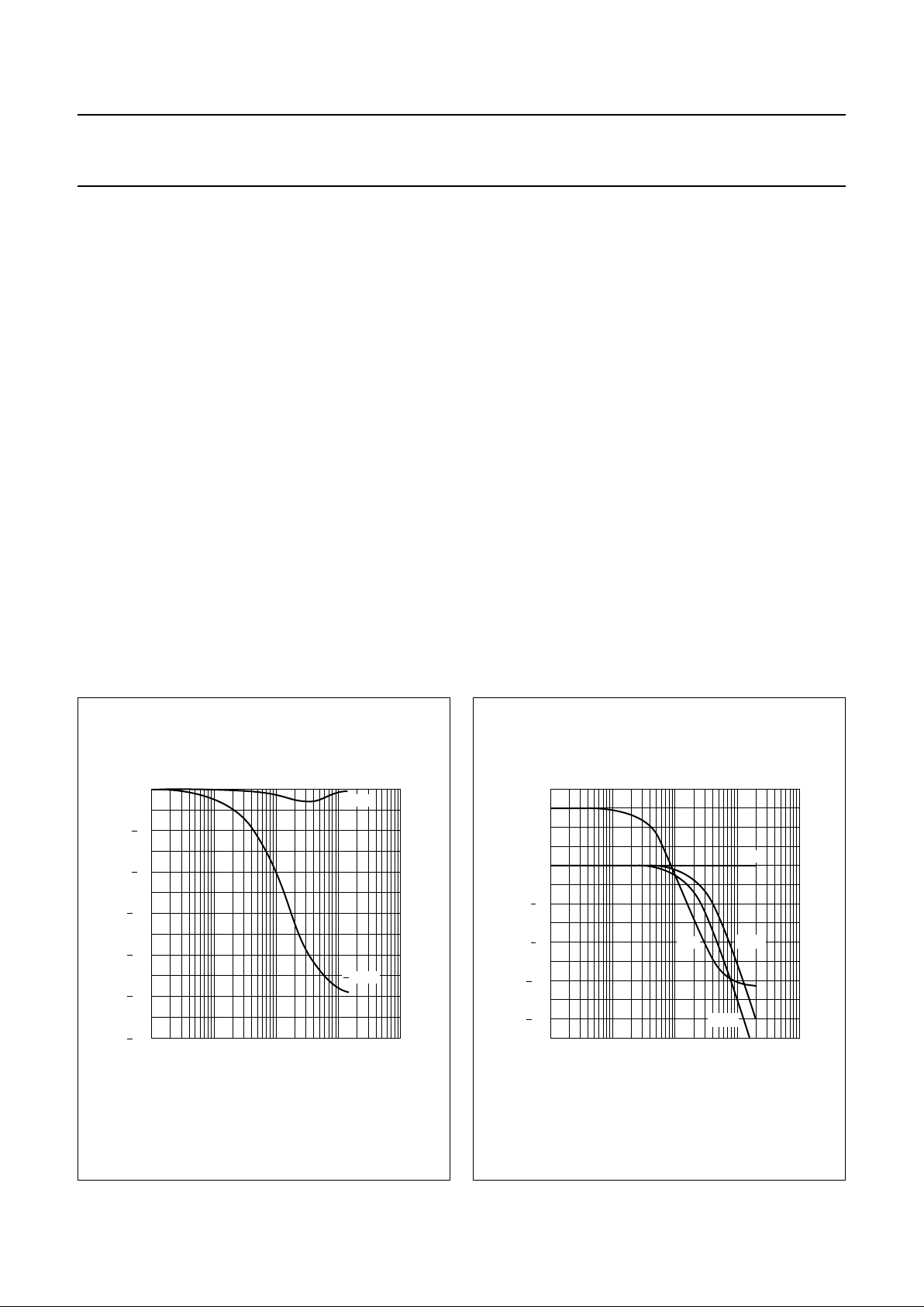
Noise Reduction (NR)
To improve the quality of the secondary channels, the
audio signal is processed at the transmitter side before
modulation. For an overall flat audio response the inverse
processing must take place after demodulation. This is
achieved in the NR.
The NR can be regarded as an input level dependent
Low-Pass Filter (LPF) [adaptive de-emphasis system]
followed by a fixed de-emphasis. Figure 3 shows the
transfer characteristics as function of the input level
(normalized to input level, and without the fixed
de-emphasis).
At maximum input level (50 kHz frequency deviation,
referred to as 0 dB) the frequency response of the first part
(i.e. without fixed de-emphasis) is nearly flat (note the
small dip around 3 kHz in Fig.3; this is a system attribute).
As the input level is X dB lowered, the higher output
frequencies will be reduced an extra X dB with respect to
the lower frequencies (1 : 2 expansion).
If a main carrier signal is received, the NR can be
bypassed at which the signal is fed directly to the
de-emphasis circuit. The noise reduction is active when
the NR signal (via I
2
C-bus) is logic 1.
De-emphasis
De-emphasis is realized by means of several internal
resistors and an external capacitor to ground. Via the
I
2
C-bus, the DEM signal can be switched between 50 µs,
75 µs, J17 and no de-emphasis. Figure 4 shows these
four different possibilities.
Output selection
With the output selector the output pins 23 and 22 can be
switched to the left and right satellite channels
(pins 33 and 31) or to the external inputs (pins 25 and 24)
for an other signal source or for connection of a decoder
box. the OS1 and OS0 bits determine this selection.
Pin 21 is a separate output which delivers the mono
channel. The mono signal is the sum of pin 23 (left) and
pin 22 (right) output signal [
1
⁄2(l + r)].
Page 10
1996 Mar 11 10
Philips Semiconductors Preliminary specification
Satellite sound receiver with I2C-bus control
TDA8745
Output pins 23 and 22 can be muted by setting the
OML and OMR signals to logic 1. In addition, automatic
muting is also possible, the presence detector (as
described in Section “Presence detector”) sets the PDL bit
(PDR for other channel). Absence of a carrier at the
selected frequency results in automatic muting. This
mechanism is enabled or inhibited by the PDM bit
(Presence Detector auto Mute).
All outputs (pins 21, 22 and 23) are line drivers with
SCART level capability and are short-circuit protected by
means of 125 Ω output resistors. Pins 34 and 30 are also
line drivers at SCART level and can be used as signal
outputs before the IC’s output selection (i.e. for decoder
box use).
ABBREVIATIONS
BPF = Band-Pass Filter.
f
mod
= modulating frequency.
∆fM= frequency deviation of the main Channel.
∆fS1= frequency deviation of secondary Channel 1 (left).
∆fS2= frequency deviation of secondary Channel 2 (right).
f
OM
= carrier frequency of main Channel.
f
OS1
= carrier frequency of secondary Channel 1.
f
OS2
= carrier frequency of secondary Channel 2.
IF = Intermediate Frequency.
IL = Input Left.
IR = Input Right.
LPF = Low-Pass Filter.
NR = Noise Reduction.
OML = Output Mute Left.
OMR = Output Mute Right.
OS = Output Select.
PDM = Presence Detector auto Mute.
PE = Port Extension.
PLL = Phase-Locked Loop.
POR = Power-On Reset.
S/N = Signal-to-Noise ratio.
VCO = Voltage Controlled Oscillator.
handbook, halfpage
10
5
MBE284
10
4
10
3
10
2
10
4
0
8
12
16
20
24
transfer
(dB)
f (Hz)
20 dB
0 dB
Fig.4 Noise reduction transfer as function of
input level.
handbook, halfpage
10
5
MBE285
10
4
10
3
10
2
10
4
0
4
8
8
12
16
transfer
(dB)
f (Hz)
50 µs
75 µs
flat
J17
Fig.5 LF de-emphasis curves.
Page 11

1996 Mar 11 11
Philips Semiconductors Preliminary specification
Satellite sound receiver with I2C-bus control
TDA8745
I2C-BUS PROTOCOL
Table 1 Slave receiver/transmitter address: D4 or D6 (HEX)
Notes
1. AS bit defined by level at address select (pin 12); 0 V = logic 0; 5 V = logic 1.
2. R/W = 0; TDA8745 is receiver (microcontroller is master transmitter).
R/W = 1; TDA8745 is transmitter (microcontroller is master receiver).
TDA8745 receiver use
In the receiver mode the device has four subaddresses with auto-increment, as shown in Tables 2 to 5.
Table 2 Input byte SA: 00; situation after POR
Table 3 Tuning byte SA: 01; situation after POR
Table 4 Select byte SA: 02; situation after POR
Table 5 Audio byte SA: 03; situation after POR
TDA8745 transmitter use
No subaddress.
Table 6 Read byte
BIT 7 BIT 6 BIT 5 BIT 4 BIT 3 BIT 2 BIT 1 BIT 0
110101AS
(1)
R/W
(2)
IL2
i7
IL1
i6
IL0
i5
IR2
i4
IR1
i3
IR0
i2
TUN9
i1
TUN8
i0
00000110
TUN7
t7
TUN6
t6
TUN5
t5
TUN4
t4
TUN3
t3
TUN2
t2
TUN1
t1
TUN0
t0
11101100
TEST
s7
BB
s6
OS1
s5
OS0
s4
PDM
s3
PE
s2
OML
s1
OMR
s0
00000011
LEV3
a7
LEV2
a6
LEV1
a5
LEV0
a4
NR
a3
DEM1
a2
DEM0
a1
BPFN
a0
11001110
PDL
r7
PDR
r6
−
r5
−
r4
−
r3
−
r2
−
r1
POR
r0
0 or 10 or 1111110 or 1
Page 12

1996 Mar 11 12
Philips Semiconductors Preliminary specification
Satellite sound receiver with I2C-bus control
TDA8745
Slave receiver mode (bits transmitted from microcontroller to TDA8745)
Different IF inputs can be selected for the PLLs, for switching between different external BPFs and/or channels;
see Tables 7 and 8.
Table 7 IL2 to IL0; Input Left; note 1
Notes
1. X = don’t care.
2. Bit PE (s2) can be set to logic 1 to change IF input 5 into digital output for external switching purposes.
IL2
i7
IL1
i6
IL0
i5
PE
(2)
s2
MODE
0000IF input IN-1 selected for left PLL (after POR)
0010IF input IN-2 selected for left PLL
0100IF input IN-3 selected for left PLL
0110IF input IN-4 selected for left PLL
1000IF input IN-5 selected for left PLL
1010IF input IN-6 selected for left PLL
1100no selection
1110no selection
X 0 0 1 IF input IN-1 selected for left PLL
X 0 1 1 IF input IN-2 selected for left PLL
X 1 0 1 IF input IN-3 selected for left PLL
X 1 1 1 IF input IN-4 selected for left PLL
0 X X 1 IF input IN-5 used as output; 0 = 0 V
1 X X 1 IF input IN-5 used as output; 1 = 5 V
Page 13

1996 Mar 11 13
Philips Semiconductors Preliminary specification
Satellite sound receiver with I2C-bus control
TDA8745
Table 8 IR2 to IR0; input right; note 1
Notes
1. X = don’t care.
2. Bit PE (s2) can be set to logic 1 to change IF input 6 into digital output for external switching purposes.
IR2
i4
IR1
i3
IR0
i2
PE
(2)
s2
MODE
0000IF input IN-1 selected for right PLL
0010IF input IN-2 selected for right PLL (after POR)
0100IF input IN-3 selected for right PLL.
0110IF input IN-4 selected for right PLL
1000IF input IN-5 selected for right PLL
1010IF input IN-6 selected for right PLL
1100no selection
1110no selection
X 0 0 1 IF input IN-1 selected for right PLL
X 0 1 1 IF input IN-2 selected for right PLL
X 1 0 1 IF input IN-3 selected for right PLL
X 1 1 1 IF input IN-4 selected for right PLL
0 X X 1 IF input IN-6 used as output; 0 = 0 V
1 X X 1 IF input IN-6 used as output; 1 = 5 V
Page 14

1996 Mar 11 14
Philips Semiconductors Preliminary specification
Satellite sound receiver with I2C-bus control
TDA8745
Table 9 TUN9 to TUN0; tuning
Note
1. This is the situation after POR.
The frequency range of synthesizer is shown in Table 10.
Table 10 Frequency range of synthesizer
Notes
1. Tuning the synthesizer below 29.04 MHz may be possible, but is not guaranteed.
2. The mixing frequency (f
mix
) can be calculated with equation:
f
mix
= (1024 + 512[TUN9] + 256[TUN8] + 128[TUN7] + 64[TUN6] + 32[TUN5] + 16[TUN4] + 8[TUN3] + 4[TUN2] +
2[TUN1] + [TUN0]) × 10 kHz.
3. Tuning frequency = mixer input frequency − 10.7 MHz.
TUN9i1TUN8i0TUN7t7TUN6t6TUN5t5TUN4t4TUN3t3TUN2t2TUN1t1TUN0
t0
10.7 IF
(MHz)
10.52 IF
(MHz)
0110101100 3.82 4.00
0110101101 3.83 4.01
0110101110 3.84 4.02
0110101111 to 1001010011 3.85 to 5.49 4.03 to 5.67
1001010100 5.50 5.68
1001010101 to 1010000101 5.51 to 5.99 5.69 to 6.17
1010000110 6.00 6.18
1010000111 to 1010110111 6.01 to 6.49 6.19 to 6.67
1010111000 6.50 6.68
1010111001 to 1011101011 6.51 to 7.01 6.69 to 7.19
10111011007.02
(1)
7.20
(1)
1011101101 to 1100001111 7.03 to 7.37 7.21 to 7.55
1100010000 7.38 7.56
1100010001 to 1100110011 7.39 to 7.73 7.57 to 7.91
1100110100 7.74 7.92
1100110101 to 1111111100 7.75 to 9.74 7.93 to 9.92
1111111101 9.75 9.93
1111111110 9.76 9.94
1111111111 9.77 9.95
PARAMETER
RANGE
(MHz)
Synthesizer frequency range 29.04 to 40.94 (in 20 kHz grid); note 1
Mixer input frequency range 14.52 to 20.47 (in 10 kHz grid); note 2
Tuning range 3.82 to 9.77 (in 10 kHz grid; 10.7 MHz IF); note 3
Page 15

1996 Mar 11 15
Philips Semiconductors Preliminary specification
Satellite sound receiver with I2C-bus control
TDA8745
Table 11 Bit TEST
Table 12 Bit BB; baseband; note 1
Note
1. The PLL demodulators can also be used for demodulating FM carriers (e.g. terrestrial TV sound) at baseband
frequencies, by changing the lock range of the PLLs.
Table 13 Bits OS1 and OS0; output select; note 1
Note
1. The signal at both line outputs O
L
and OR (pins 23 and 22) can be selected with bits OS1 and OS0.
Table 14 Bit PDM; Presence Detector auto Mute; note 1
Note
1. In both situations the status of the presence detector can be monitored by reading the bits PDL (r7) and PDR (r6)
back from the IC. Appropriate action (e.g. muting, channel selection or tuning) can then be taken by the
microcontroller. Note that this function also mutes the signal from the external inputs (pins 25 and 24). This may be
desirable when using these inputs for connecting a satellite descrambler box. If not, reset PDM (s3) to logic 0 when
selecting external [e.g. together with bits OS1 (s5) and OS0 (s4)].
TEST
s7
MODE DESCRIPTION
0 − (POR) in applications this bit should always be logic 0, to avoid conflicts with other settings
1 test setting TEST enables some special modes used for factory testing
BB
s6
MODE DESCRIPTION
0 synthesizer synthesizer use (PLLs central frequency approximately 10.7 MHz) (after POR)
1 baseband baseband use (PLLs central frequency approximately 6 MHz)
OS1
s5
OS0
s4
MODE DESCRIPTION
0 0 stereo (POR) Left channel audio (pin 33) at O
L
; right channel audio (pin 31) at O
R
0 1 left Left channel audio (pin 33) at both OLand O
R
1 0 right Right channel audio (pin 31) at both OLand O
R
1 1 external External left at (pin 25) at OL; external right (pin 24) at O
R
PDM
s3
MODE DESCRIPTION
0 − (POR) −
1 PDM if this bit is set to logic 1, a channel for which no incoming carrier is found will be muted
Page 16

1996 Mar 11 16
Philips Semiconductors Preliminary specification
Satellite sound receiver with I2C-bus control
TDA8745
Table 15 Bit PE; Port Extension; note 1
Note
1. Two IF inputs (IN-5 and IN-6; pins 7 and 8) can be used as digital output instead. If no more than four IF inputs are
needed, two external functions can be controlled via the I2C-bus this way. The level at these pins is controlled by
bits IL2 (i7) and IR2 (i4); see Tables 7 and 8.
Table 16 Bits OML and OMR; Output Mute Left and Output Mute Right; note 1
Note
1. Left and right audio can be muted independently. Note that also the external input signals (pins 25 and 24) can be
muted this way.
PE
s2
DESCRIPTION
0 6 IF inputs; no digital output (after POR)
1 4 IF inputs; 2 digital outputs
BIT LEVEL MODE DESCRIPTION
OML (s1) 0 −−
1 mute Left audio channel is muted
OMR (s0) 0 −−
1 mute Right audio channel is muted
Page 17

1996 Mar 11 17
Philips Semiconductors Preliminary specification
Satellite sound receiver with I2C-bus control
TDA8745
Table 17 Bits LEV3 to LEV0; level adjust; note 1
Notes
1. The audio level can be adjusted in steps of 1 dB, to adjust for different FM deviations used in main channel audio
carriers and/or spread in PLL output amplitude. With secondary carriers the Noise Reduction (NR) is to be used with
the 0 dB setting (note that the NR audio frequency response is level dependent, therefore another setting than 0 dB
is only to be used when making a fine-adjustment (+2 dB/−2 dB) for PLL spread. Typical setting for main channel
carriers is in most cases 85 kHz (0 dB) or 76 kHz (+1 dB).
2. Maximum deviation.
3. Situation after POR.
Table 18 Bit NR; Noise Reduction; note 1
Note
1. For reception of main channel carriers the NR circuit can be bypassed.
LEV3
a7
LEV2
a6
LEV1
a5
LEV0
a4
MODE
SECONDARY
CHANNELS
(2)
(kHz)
MAIN CHANNEL
(2)
(kHz)
0000−12 dB 199 338
0001−11 dB 177 302
0010−10 dB 158 269
0011−9 dB 141 240
0100−8 dB 126 214
0101−7 dB 112 190
0110−6 dB 100 170
0111−5 dB 89 151
1000−4 dB 79 135
1001−3 dB 71 120
1010−2 dB 63 107
1011−1dB 56 95
1100 0dB 50
(3)
85
(3)
1101+1dB 45 76
1110+2dB 40 68
1111+3dB 35 60
NR
a3
MODE DESCRIPTION
0 NR bypassed Noise Reduction bypassed (main channel)
1 NR active Noise Reduction active (secondary channels) (after POR)
Page 18

1996 Mar 11 18
Philips Semiconductors Preliminary specification
Satellite sound receiver with I2C-bus control
TDA8745
Table 19 Bits DEM1 and DEM0; De-emphasis; note 1;
see Fig.5
Notes
1. Different de-emphasis characteristics can be selected,
to adjust for different main channel audio carriers.
2. In most cases the de-emphasis needed for main
channel carriers is 50 µs.
3. The NR is to be used with the 75 µs setting for
standard secondary channels.
Table 20 Bit BPFN; Band-Pass Filter Not; note 1
Note
1. To avoid interference by the video signal, the incoming
baseband signal is filtered. If this filtering is not
required the filter can be switched off.
DEM1
a2
DEM0
a1
DE-EMPHASIS
0 0 no de-emphasis (flat)
0 1 J17
1050µs
(2)
1175µs [por]
(3)
BPFN
a0
DESCRIPTION
0 mixer input signal filtered by BPF
(after POR)
1 mixer input signal is not filtered
Slave transmitter mode (bits transmitted from
TDA8745 to microcontroller)
Table 21 Bit PDL; Presence Detector Left; note 1
Note
1. Bit PDL (r7) transmits the current status of the left
channel presence detector. When PDL = 1, no carrier
is found at the currently selected frequency. If bit
PDM (s3) = 0 the left channel audio is muted.
Table 22 Bit PDR; Presence Detector Right; note 1
Note
1. Bit PDR (r6) transmits the current status of the right
channel presence detector. When PDR = 1, no carrier
is found at the currently selected frequency. If bit
PDM (s3) = 0 the right channel audio is muted.
PDL
r7
DESCRIPTION
0 carrier detected at left channel
1 no carrier detected at left channel
PDR
r6
DESCRIPTION
0 carrier detected at right channel
1 no carrier detected at right channel
Table 23 Bit POR; Power-On Reset; note 1
Note
1. At switching on, or after a power dip on the I2C-bus supply voltage (VP2), an internal signal is generated which resets
the I2C-bus registers to a pre-defined state. If bit POR (r0) = 1, such a situation has occurred since the last time the
read byte was read. After reading, the bit is reset to logic 0.
Table 24 Bits r5 to r1
POR
r0
DESCRIPTION
0 normal operation
1 POR generated; power dip detected since last read of POR bit
−
r5
−
r4
−
r3
−
r2
−
r1
DESCRIPTION
11111These bits have no function. Although their state is fixed, the microcontroller
should not rely on this because of eventual future use.
Page 19

1996 Mar 11 19
Philips Semiconductors Preliminary specification
Satellite sound receiver with I2C-bus control
TDA8745
LIMITING VALUES
In accordance with the Absolute Maximum Rating System (IEC 134).
Notes
1. All voltages referenced to ground at pins 6, 10, 14 and 32.
2. Port Extension enabled (PE = 1; see Table 15).
3. IN-5 and IN-6 (pins 7 and 8) not being in the Port Extension mode.
THERMAL CHARACTERISTICS
SYMBOL PARAMETER CONDITIONS MIN. MAX. UNIT
V
P1
synthesizer and mixer supply voltage note 1 0 5.5 V
V
P2
I2C-bus supply voltage note 1 0 5.5 V
V
P3
general supply voltage note 1 0 13.2 V
V
n
voltage on pins 2, 3, 5 and 40 note 1 0 5.5 V
voltage on pins 7 and 8 note 2 0 V
P2
V
voltage on pins 1 and 42 note 1 0 7.7 V
V
i
input voltage on pins 7, 8, 9, 11,13 and 15 notes 1 and 3 0 1 V
T
stg
storage temperature −65 +150 °C
T
amb
operating ambient temperature −20 +70 °C
SYMBOL PARAMETER VALUE UNIT
R
th j-a
thermal resistance from junction to ambient in free air
SDIP42 50 K/W
QFP44 60 K/W
Page 20

1996 Mar 11 20
Philips Semiconductors Preliminary specification
Satellite sound receiver with I2C-bus control
TDA8745
DC CHARACTERISTICS
All voltages referenced to ground (pins 6, 10, 14 and 32). In accordance with the block diagram (see Fig.1);
VP1=VP2=5V; VP3=12V; T
amb
=25°C; f
OS1
= 10.7 MHz; f
OS2
= 10.52 MHz (no modulation; see note 1); unless
otherwise specified.
Notes
1. Presence of both carriers is required to achieve lock of the PLLs; otherwise not all pins will have a stable DC voltage.
2. Pin 7 and 8 functioning as normal inputs (bit PE = 0).
SYMBOL PARAMETER CONDITIONS MIN. TYP. MAX. UNIT
Supply
V
P1
synthesizer and mixer supply voltage 4.5 5.0 5.5 V
V
P2
I2C-bus supply voltage 4.5 5.0 5.5 V
V
P3
general supply voltage 8.0 12 13.2 V
I
P1
synthesizer and mixer supply current − 37 48 mA
I
P2
I2C-bus supply current − 0.6 − mA
I
P3
general supply current − 35 46 mA
P
tot
total power dissipation − 610 800 mW
Pins
V
21,22,23
voltage on pins 21, 22 and 23 − 3.8 − V
V
24,25,31,33
voltage on pins 24, 25, 31 and 33 − 3.8 − V
V
31,33
voltage on pins 31 and 33 − 3.8 − V
V
30,34
voltage on pins 30 and 34 − 3.8 − V
V
27,37
voltage on pins 27 and 37 − 3.8 − V
V
19
voltage on pin 19 3.7 3.8 3.9 V
V
9,11,13,15
voltage on pins 9, 11, 13 and 15 note 2 − 0 − V
V
42,1
voltage on pins 42 and 1 − 3.4 − V
V
41,39
voltage on pins 41 and 39 − 2.6 − V
V
5
voltage on pin 5 − 1.8 − V
V
3
voltage on pin 3 − 2.4 − V
V
2
voltage on pin 2 − 2.6 − V
V
40
voltage on pin 40 − 1.3 − V
Port extensions (pins 7 and 8; bit PE = 1)
V
OH
HIGH level output voltage IOH= 0.5 mA 4.5 − 5V
V
OL
LOW level output voltage IOL= −0.5 mA 0 − 0.5 V
Page 21

1996 Mar 11 21
Philips Semiconductors Preliminary specification
Satellite sound receiver with I2C-bus control
TDA8745
AC CHARACTERISTICS
All voltages referenced to ground (pins 6, 10, 14 and 32); in accordance with the block diagram (see Fig.1);
VP1=VP2=5V; VP3=12V; T
amb
=25°C; f
mod
= 1 kHz; ∆fM= 46 kHz; ∆fS1= ∆fS2= 27 kHz (reference levels);
fOM= 10.7 MHz; f
OS1
= 10.7 MHz; f
OS2
= 10.52 MHz; IF level at pins 9, 11,13, 15, 7 and8=20mV (RMS value) and
SFE 10.7MJA (narrow), SFE 10.52MJA (narrow) and SFE 10.7MS3 (wide) ceramic filters; unless otherwise specified.
SYMBOL PARAMETER CONDITIONS MIN. TYP. MAX. UNIT
Band-pass filter, mixer and buffer
R
i
input resistance 10 12.5 15 kΩ
V
i(rms)
baseband input voltage (RMS value) note 1 −−200 mV
V
3
1 dB compression point (RMS value) ∆V3−∆V5= 1 dB; note 2 − 180 − mV
H
l/Hh
filter transfer at 200 kHz
with respect to 7.3 MHz
−−−60 dB
H
lm/Hh
filter transfer at 2 MHz
with respect to 7.3 MHz
−−28 −20 dB
H
mh/Hh
filter transfer at 5.3 MHz
with respect to 7.3 MHz
−2+2+4dB
H
h
*A filter transfer at 7.3 MHz and
mixer amplification
15 17 19 dB
H
h
*C filter transfer at 7.3 MHz and
mixer conversion gain
note 3 10 12 14 dB
I
o(p)
mixer output current (peak) 5 7 − mA
R
o
mixer output resistance f = 10.7 MHz; note 4 − 12 30 Ω
Charge pump, buffer amplifier and VCO
t repetition time of charge pump pulses − 50 −µs
S
VCO
VCO sensitivity note 5 −−9−MHz/V
f
VCO
VCO frequency V
loopf
= 2.6 V − 35.4 − MHz
Crystal oscillator (4 MHz)
f
xtal
crystal oscillator frequency − 4 − MHz
R
xtal
resonance resistance of crystal −−60 Ω
C
xtal
parallel capacitance of crystal − 4.5 10 pF
I
i(p)
input current from external 4 MHz
source (peak)
note 6 50 −−µA
IF inputs (pins 9, 11, 13, 15, 7 and 8) and limiters
V
IN-1 to IN-6(rms)
input sensitivity (RMS value) S/N(A) = 40 dB;
∆fS= 27 kHz; NR = on;
de-emphasis = 75 µs
− 0.3 1 mV
S/N(A) = 40 dB;
∆f
M
= 46 kHz; NR = off;
de-emphasis = 50 µs
− 0.8 2 mV
V
i1
to V
i6
input signal THD ≤ 0.5% −−200 mV
Page 22

1996 Mar 11 22
Philips Semiconductors Preliminary specification
Satellite sound receiver with I2C-bus control
TDA8745
PLL FM demodulators
f
CCO
free-running frequency PLL left; BB = 0 − 10.6 − MHz
PLL right; BB = 0 − 10.6 − MHz
PLL left; BB = 1 − 6.9 − MHz
PLL right; BB = 1 − 6.9 − MHz
∆f
CCO
lock range of PLLs BB= 0; note 7 10 − 11.5 MHz
BB = 1; note 7 5.50 − 8.50 MHz
V
OL
; V
OR
PLL output voltage (pins 23 and 22) NR = off; DEEM = flat;
BB = 0
−−5.6 − dBV
NR = off; DEEM = flat;
BB = 1; note 8
−−7.3 − dBV
∆VOL; ∆V
OR
spread of PLL output voltage over
lock range (pins 23 and 22)
NR = off; DEEM = flat;
BB = 1; note 8
−−±1.5 dB
Noise reduction
low-pass filter 50 kHz response
with respect to 1 kHz
note 9 −21 −16 −11 dB
V
o 23,22
output voltage (pins 23 and 22) at 0 dB NR input level;
∆fS1= ∆fS2= 50 kHz;
DEEM = flat; note 10
−1+1+3dBV
at −20 dB NR input level;
∆f
S1
= ∆fS2= 5 kHz;
DEEM = flat
−29 −26 −23 dBV
15 kHz frequency response
with respect to 1 kHz
at 0 dB NR input level;
∆f
S1
= ∆fS2= 50 kHz;
DEEM = flat
−2 0 +2 dB
at −20 dB NR input level;
∆f
S1
= ∆fS2= 5 kHz;
DEEM = flat
−13 −11.5 −10 dB
V
offset(DC)
DC offset voltage on attack/recovery
capacitors (pins 38 and 26)
∆f = 0 kHz; all PLLs locked 14 − 22 mV
De-emphasis
15 kHz frequency response
with respect to 1 kHz flat
NR = off; DEEM = flat −0.5 0.0 +0.5 dB
NR = off; DEEM = J17;
note 11
−13.9 −12.4 −10.9 dB
NR = off; DEEM = 50 µs −15.2 −13.7 −12.2 dB
NR = off; DEEM = 75 µs −18.6 −17.1 −15.6 dB
R
o
output resistance (pins 34 and 30) 100 125 150 Ω
SYMBOL PARAMETER CONDITIONS MIN. TYP. MAX. UNIT
V
37,27 (50 kHz)
V
37,27 (1 kHz)
---------------------------------
V
23,22 (15 kHz)
V
23,22 (1 kHz)
--------------------------------- -
V
23,22 (15 kHz)
V
23,22 (1 kHz)
--------------------------------- -
Page 23

1996 Mar 11 23
Philips Semiconductors Preliminary specification
Satellite sound receiver with I2C-bus control
TDA8745
Overall performance
V
i 3(rms)
baseband input sensitivity main
sound carrier (RMS value)
S/N(A) = 40 dB;
∆fS= 27 kHz; NR = on;
DEEM = 75 µs
− 0.5 1.5 mV
S/N(A) = 40 dB;
∆f
M
= 46 kHz; NR = off;
DEEM = 50 µs
− 1.5 3 mV
V
o 23,22
output voltage secondary channels;
∆fS= 27 kHz; NR = on;
DEEM = 75 µs
−8 −6 −4 dBV
main channel;
∆f
S
= 46 kHz; NR = off;
DEEM = 50 µs
−8 −6 −4 dBV
UBS unbalance output voltage secondary channels;
NR = on; DEEM = 75 µs
−1 − +1 dBV
main channel; NR = off;
DEEM = 50 µs
−1 − +1 dBV
THD total harmonic distortion secondary channels;
NR = on; DEEM = 75 µs;
note 12
− 0.1 0.5 %
main channel; NR = off;
DEEM = 50 µs; note 12
− 0.1 0.5 %
S/N(A) signal-to-noise ratio A-weighted; secondary
channels (synthesizer
included); NR = on;
DEEM = 75 µs; note 12
69 77 − dB
A-weighted; secondary
channels (synthesizer
excluded); NR = on;
DEEM = 75 µs; note 12
72 80 − dB
A-weighted; main channel
(synthesizer included);
NR = off; DEEM = 50 µs;
note 12
54 62 − dB
A-weighted; main channel
(synthesizer excluded);
NR = off; DEEM = 50 µs;
note 12
62 70 − dB
MUTE
att
mute attenuation output select left and right
muted
74 90 − dB
α
ct S/S
crosstalk attenuation between
secondary channels
− 74 − dB
SVRR
P3
supply voltage ripple rejection VRR= 100 mV; fi= 70 Hz;
NR = on; DEEM = 75 µs
− 14.3 − dB
V
RR
= 100 mV; fi= 1 kHz;
NR = on; DEEM = 75 µs
− 15.6 − dB
SYMBOL PARAMETER CONDITIONS MIN. TYP. MAX. UNIT
Page 24

1996 Mar 11 24
Philips Semiconductors Preliminary specification
Satellite sound receiver with I2C-bus control
TDA8745
Notes
1. Maximum of 0.5% THD at LF outputs.
2. When the increase of the output signal (pin 5 at 10.7 MHz) lags 1 dB behind the increase of the input signal
(pin 3; 7.02 MHz carrier), the so called 1 dB compression point is reached. For complex signals (more than one
sound carrier), this point will shift to a higher value.
3. The mixer performs both a mixing and amplifying action (normal operation). The synthesizer is tuned to the 7.3 MHz
incoming carrier.
4. The buffer output is sensitive to capacitive loading, therefore (capacitive) loads other than those present in the block
diagram (see Fig.1) should be avoided.
5. As present at the mixer output (pin 5) in ‘BPFTILT’ test mode the actual VCO sensitivity is two times the given value
because of the divide-by-two circuit between VCO output and mixer.
6. The required 4 MHz crystal can be omitted if this frequency is already available in the application. This signal source
should be connected to pin 40, via a capacitor in series with a resistor R
ext
. The minimum required AC current is
50 µA, determined by the resistors R
int
and R
ext
and the level of the 4 MHz AC voltage. The value of R
int
is 700 Ω
and the signal shape of the signal is not important.
SVRR
P1-P2
supply voltage ripple rejection VRR= 100 mV; fi= 70 Hz;
NR = on; DEEM = 75 µs
− 25 − dB
V
RR
= 100 mV; fi= 1 kHz;
NR = on; DEEM = 75 µs
− 4 − dB
Output select
V
i 25,24
input voltage (pins 25 and 24) −−8 dBV
R
i 25,24,33,31
input resistance at
pins 25, 24, 33 and 31
100 150 200 kΩ
V
o 23,22
output voltage at pins 23 and 22 V
24,25
= −6 dBV;
OS = external
−6.5 −6 −5.5 dBV
R
o 23,22,21
output resistance at
pins 23, 22 and 21
100 125 150 Ω
THD total harmonic distortion V
24,25
= −6 dBV;
OS = external; f=1kHz
− 0.01 0.3 %
S/N(A) signal-to-noise ratio A-weighted;
V
24,25
= −6 dBV;
OS = external
80 −−dB
α
ct L/R
; α
ct R/L
crosstalk between channels f = 1 kHz − 80 − dB
I
2
C-bus
C
i
input capacitance − 4 − pF
I
sink
SDA sink current 3 −−mA
V
IH
HIGH level input voltage 3 − 5V
V
IL
LOW level input voltage 0 − 1.5 V
I
IH
HIGH level input current −−10 µA
I
IL
LOW level input current −−10 µA
Address D4H address D4H ADD
sel
= LOW 0 − 1V
Address D6H address D6H ADD
sel
= HIGH 3 − 5V
f
SCL
SCL frequency −−100 kHz
SYMBOL PARAMETER CONDITIONS MIN. TYP. MAX. UNIT
Page 25

1996 Mar 11 25
Philips Semiconductors Preliminary specification
Satellite sound receiver with I2C-bus control
TDA8745
7. Maximum THD of 0.5%; 8 V < VP3< 13.2 V; 0 °C<T
amb
<70°C. Measured at pins 34 and 30; NR = off;
DEEM = flat.
8. Correction of output voltage is possible by correcting the volume level.
9. Measured at pins 37 and 27 with no electrolytic capacitors connected to these pins.
10. Input level of 0 dB; signal level in accordance with ∆fS1= ∆fS2= 50 kHz. At this input level, the NR response is equal
for high and low frequencies (see Fig.4).
11. J17 de-emphasis includes +6 dB amplification (see Fig.5).
12. Both PLLs locked.
INTERNAL CIRCUITRY
For description see Chapter “Pinning”.
SYMBOL PIN EQUIVALENT CIRCUIT
C
DC R
1
SLF 2
MLD094
1
1640 Ω
20 Ω
1640 Ω
20 Ω
MLD095
2
2 kΩ
2 kΩ 1 kΩ
2 kΩ
275 Ω
Page 26

1996 Mar 11 26
Philips Semiconductors Preliminary specification
Satellite sound receiver with I2C-bus control
TDA8745
BASEBAND IN 3
V
P1
4
IF OUT 5
SYNGND 6
IN-5 7
SYMBOL PIN EQUIVALENT CIRCUIT
3
MLD096
12.5 kΩ
2.5 V
4V
MLD060
P1
5
MLD061
MLD062
6
SYNGND
MLD063
7
275 Ω
Page 27

1996 Mar 11 27
Philips Semiconductors Preliminary specification
Satellite sound receiver with I2C-bus control
TDA8745
IN-6 8
IN-1 9
HFGND 10
IN-2 11
ADD
sel
12
SYMBOL PIN EQUIVALENT CIRCUIT
MLD097
8
275 Ω
MLD064
9
275 Ω
MLD065
10
HFGND
MLD066
11
275 Ω
MLD067
12
275 Ω
Page 28

1996 Mar 11 28
Philips Semiconductors Preliminary specification
Satellite sound receiver with I2C-bus control
TDA8745
IN-3 13
I2CGND 14
IN-4 15
V
P2
16
SCL 17
SDA 18
SYMBOL PIN EQUIVALENT CIRCUIT
MLD114
13
275 Ω
MLD068
14
I CGND
2
MLD098
15
275 Ω
MLD069
16
V
P2
MLD070
17
275 Ω
MLD071
18
275 Ω
Page 29

1996 Mar 11 29
Philips Semiconductors Preliminary specification
Satellite sound receiver with I2C-bus control
TDA8745
V
ref
19
V
P3
20
O
M
21
O
R
22
SYMBOL PIN EQUIVALENT CIRCUIT
MLD072
19
15.2 kΩ
40 kΩ
125 Ω
275 Ω
25 Ω
MLD073
20
V
P3
MLD074
125 Ω
21
3.8 V
MLD075
125 Ω
22
3.8 V
Page 30

1996 Mar 11 30
Philips Semiconductors Preliminary specification
Satellite sound receiver with I2C-bus control
TDA8745
O
L
23
EXT
R
24
EXT
L
25
C
ATT/RECR
26
SYMBOL PIN EQUIVALENT CIRCUIT
MLD076
125 Ω
23
3.8 V
MLD077
20 Ω 103 kΩ
3.8 V 3.8 V
24
I
O
I
O
transfer gate
transfer gate
47 kΩ
MLD078
20 Ω 103 kΩ
3.8 V 3.8 V
25
I
O
I
O
transfer gate
transfer gate
47 kΩ
26
MLD079
100 Ω
100 Ω
3.8 V
Page 31

1996 Mar 11 31
Philips Semiconductors Preliminary specification
Satellite sound receiver with I2C-bus control
TDA8745
RECT
R
27
C
NR D R
28
C
DR
29
DEEM OUT R 30
C
CL R
31
SYMBOL PIN EQUIVALENT CIRCUIT
MLD080
4.7 kΩ
27
28
MLD081
7.5 kΩ
275 Ω
AC signal current
MLD082
3.8 V
I
O
I
O
transfer gate
transfer gate
125 Ω
29
30
MLD083
20 Ω 103 kΩ
3.8 V 3.8 V
31
I
O
I
O
transfer gate
transfer gate
47 kΩ
Page 32

1996 Mar 11 32
Philips Semiconductors Preliminary specification
Satellite sound receiver with I2C-bus control
TDA8745
AFGND 32
C
CL L
33
DEEM OUT L 34
C
DL
35
C
NR D L
36
SYMBOL PIN EQUIVALENT CIRCUIT
MLD084
32
AFGND
substrate
MLD085
20 Ω 103 kΩ
3.8 V 3.8 V
33
I
O
I
O
transfer gate
transfer gate
47 kΩ
MLD086
3.8 V
I
O
I
O
transfer gate
transfer gate
125 Ω
35
34
36
MLD224
7.5 kΩ
275 Ω
AC signal current
Page 33

1996 Mar 11 33
Philips Semiconductors Preliminary specification
Satellite sound receiver with I2C-bus control
TDA8745
RECT
L
37
C
ATT/RECL
38
PRES DET R 39
XTAL 40
SYMBOL PIN EQUIVALENT CIRCUIT
MLD088
4.7 kΩ
37
38
MLD089
100 Ω
100 Ω
3.8 V
MLD090
39
100 Ω
100 Ω
40
MLD091
Page 34

1996 Mar 11 34
Philips Semiconductors Preliminary specification
Satellite sound receiver with I2C-bus control
TDA8745
PRES DET L 41
C
DC L
42
SYMBOL PIN EQUIVALENT CIRCUIT
MLD092
41
100 Ω
100 Ω
MLD093
42
1640 Ω
20 Ω
1640 Ω
20 Ω
Page 35

1996 Mar 11 35
Philips Semiconductors Preliminary specification
Satellite sound receiver with I2C-bus control
TDA8745
PACKAGE OUTLINES
UNIT b
1
cEe M
H
L
REFERENCES
OUTLINE
VERSION
EUROPEAN
PROJECTION
ISSUE DATE
IEC JEDEC EIAJ
mm
DIMENSIONS (mm are the original dimensions)
SOT270-1
90-02-13
95-02-04
b
max.
w
M
E
e
1
1.3
0.8
0.53
0.40
0.32
0.23
38.9
38.4
14.0
13.7
3.2
2.9
0.181.778 15.24
15.80
15.24
17.15
15.90
1.73
5.08 0.51 4.0
M
H
c
(e )
1
M
E
A
L
seating plane
A
1
w M
b
1
e
D
A
2
Z
42
1
22
21
b
E
pin 1 index
0 5 10 mm
scale
Note
1. Plastic or metal protrusions of 0.25 mm maximum per side are not included.
(1) (1)
D
(1)
Z
A
max.
12
A
min.
A
max.
SDIP42: plastic shrink dual in-line package; 42 leads (600 mil)
SOT270-1
Page 36

1996 Mar 11 36
Philips Semiconductors Preliminary specification
Satellite sound receiver with I2C-bus control
TDA8745
UNIT A1A2A3b
p
cE
(1)
eH
E
LL
p
Zywv θ
REFERENCES
OUTLINE
VERSION
EUROPEAN
PROJECTION
ISSUE DATE
IEC JEDEC EIAJ
mm
0.25
0.05
1.85
1.65
0.25
0.40
0.20
0.25
0.14
10.1
9.9
0.8 1.3
12.9
12.3
1.2
0.8
10
0
o
o
0.15 0.10.15
DIMENSIONS (mm are the original dimensions)
Note
1. Plastic or metal protrusions of 0.25 mm maximum per side are not included.
0.95
0.55
SOT307-2
95-02-04
97-08-01
D
(1) (1)(1)
10.1
9.9
H
D
12.9
12.3
E
Z
1.2
0.8
D
e
E
B
11
c
E
H
D
Z
D
A
Z
E
e
v M
A
X
1
44
34
33 23
22
12
y
θ
A
1
A
L
p
detail X
L
(A )
3
A
2
pin 1 index
D
H
v M
B
b
p
b
p
w M
w M
0 2.5 5 mm
scale
QFP44: plastic quad flat package; 44 leads (lead length 1.3 mm); body 10 x 10 x 1.75 mm
SOT307-2
A
max.
2.10
Page 37

1996 Mar 11 37
Philips Semiconductors Preliminary specification
Satellite sound receiver with I2C-bus control
TDA8745
SOLDERING
Introduction
There is no soldering method that is ideal for all IC
packages. Wave soldering is often preferred when
through-hole and surface mounted components are mixed
on one printed-circuit board. However, wave soldering is
not always suitable for surface mounted ICs, or for
printed-circuits with high population densities. In these
situations reflow soldering is often used.
This text gives a very brief insight to a complex technology.
A more in-depth account of soldering ICs can be found in
our
“IC Package Databook”
(order code 9398 652 90011).
SDIP
SOLDERING BY DIPPING OR BY WA VE
The maximum permissible temperature of the solder is
260 °C; solder at this temperature must not be in contact
with the joint for more than 5 seconds. The total contact
time of successive solder waves must not exceed
5 seconds.
The device may be mounted up to the seating plane, but
the temperature of the plastic body must not exceed the
specified maximum storage temperature (T
stg max
). If the
printed-circuit board has been pre-heated, forced cooling
may be necessary immediately after soldering to keep the
temperature within the permissible limit.
R
EPAIRING SOLDERED JOINTS
Apply a low voltage soldering iron (less than 24 V) to the
lead(s) of the package, below the seating plane or not
more than 2 mm above it. If the temperature of the
soldering iron bit is less than 300 °C it may remain in
contact for up to 10 seconds. If the bit temperature is
between 300 and 400 °C, contact may be up to 5 seconds.
QFP
REFLOW SOLDERING
Reflow soldering techniques are suitable for all QFP
packages.
The choice of heating method may be influenced by larger
plastic QFP packages (44 leads, or more). If infrared or
vapour phase heating is used and the large packages are
not absolutely dry (less than 0.1% moisture content by
weight), vaporization of the small amount of moisture in
them can cause cracking of the plastic body. For more
information, refer to the Drypack chapter in our
“Quality
Reference Handbook”
(order code 9397 750 00192).
Reflow soldering requires solder paste (a suspension of
fine solder particles, flux and binding agent) to be applied
to the printed-circuit board by screen printing, stencilling or
pressure-syringe dispensing before package placement.
Several techniques exist for reflowing; for example,
thermal conduction by heated belt. Dwell times vary from
50 to 300 seconds depending on heating method. Typical
reflow temperatures range from 215 to 250 °C.
Preheating is necessary to dry the paste and evaporate
the binding agent. Preheat for 45 minutes at 45 °C.
W
AVE SOLDERING
Wave soldering is not recommended for QFP packages.
This is because of the likelihood of solder bridging due to
closely-spaced leads and the possibility of incomplete
solder penetration in multi-lead devices.
If wave soldering cannot be avoided, the following
conditions must be observed:
• A double-wave (a turbulent wave with high upward
pressure followed by a smooth laminar wave)
soldering technique should be used.
• The footprint must be at an angle of 45° to the board
direction and must incorporate solder thieves
downstream and at the side corners.
Even with these conditions, do not consider wave
soldering the following packages: QFP52 (SOT379-1),
QFP100 (SOT317-1), QFP100 (SOT317-2),
QFP100 (SOT382-1) or QFP160 (SOT322-1).
During placement and before soldering, the package must
be fixed with a droplet of adhesive. The adhesive can be
applied by screen printing, pin transfer or syringe
dispensing. The package can be soldered after the
adhesive is cured. Maximum permissible solder
temperature is 260 °C, and maximum duration of package
immersion in solder is 10 seconds, if cooled to less than
150 °C within 6 seconds. Typical dwell time is 4 seconds
at 250 °C.
A mildly-activated flux will eliminate the need for removal
of corrosive residues in most applications.
R
EPAIRING SOLDERED JOINTS
Fix the component by first soldering two diagonallyopposite end leads. Use only a low voltage soldering iron
(less than 24 V) applied to the flat part of the lead. Contact
time must be limited to 10 seconds at up to 300 °C. When
using a dedicated tool, all other leads can be soldered in
one operation within 2 to 5 seconds between
270 and 320 °C.
Page 38

1996 Mar 11 38
Philips Semiconductors Preliminary specification
Satellite sound receiver with I2C-bus control
TDA8745
DEFINITIONS
LIFE SUPPORT APPLICATIONS
These products are not designed for use in life support appliances, devices, or systems where malfunction of these
products can reasonably be expected to result in personal injury. Philips customers using or selling these products for
use in such applications do so at their own risk and agree to fully indemnify Philips for any damages resulting from such
improper use or sale.
PURCHASE OF PHILIPS I
2
C COMPONENTS
Data sheet status
Objective specification This data sheet contains target or goal specifications for product development.
Preliminary specification This data sheet contains preliminary data; supplementary data may be published later.
Product specification This data sheet contains final product specifications.
Limiting values
Limiting values given are in accordance with the Absolute Maximum Rating System (IEC 134). Stress above one or
more of the limiting values may cause permanent damage to the device. These are stress ratings only and operation
of the device at these or at any other conditions above those given in the Characteristics sections of the specification
is not implied. Exposure to limiting values for extended periods may affect device reliability.
Application information
Where application information is given, it is advisory and does not form part of the specification.
Purchase of Philips I
2
C components conveys a license under the Philips’ I2C patent to use the
components in the I2C system provided the system conforms to the I2C specification defined by
Philips. This specification can be ordered using the code 9398 393 40011.
Page 39

1996 Mar 11 39
Philips Semiconductors Preliminary specification
Satellite sound receiver with I2C-bus control
TDA8745
NOTES
Page 40

Philips Semiconductors – a worldwide company
Argentina: IEROD, Av. Juramento 1992 - 14.b, (1428)
BUENOS AIRES, Tel. (541)786 7633, Fax. (541)786 9367
Australia: 34 Waterloo Road, NORTH RYDE, NSW 2113,
Tel. (02)805 4455, Fax. (02)805 4466
Austria: Triester Str. 64, A-1101 WIEN, P.O. Box 213,
Tel. (01)60 101-1236, Fax. (01)60 101-1211
Belgium: Postbus 90050, 5600 PB EINDHOVEN, The Netherlands,
Tel. (31)40-2783749, Fax. (31)40-2788399
Brazil: Rua do Rocio 220 - 5
th
floor, Suite 51,
CEP: 04552-903-SÃO PAULO-SP, Brazil,
P.O. Box 7383 (01064-970),
Tel. (011)821-2333, Fax. (011)829-1849
Canada: PHILIPS SEMICONDUCTORS/COMPONENTS:
Tel. (800) 234-7381, Fax. (708) 296-8556
Chile: Av. Santa Maria 0760, SANTIAGO,
Tel. (02)773 816, Fax. (02)777 6730
China/Hong Kong: 501 Hong Kong Industrial Technology Centre,
72 Tat Chee Avenue, Kowloon Tong, HONG KONG,
Tel. (852)2319 7888, Fax. (852)2319 7700
Colombia: IPRELENSO LTDA, Carrera 21 No. 56-17,
77621 BOGOTA, Tel. (571)249 7624/(571)217 4609,
Fax. (571)217 4549
Denmark: Prags Boulevard 80, PB 1919, DK-2300
COPENHAGEN S, Tel. (45)32 88 26 36, Fax. (45)31 57 19 49
Finland: Sinikalliontie 3, FIN-02630 ESPOO,
Tel. (358)0-615 800, Fax. (358)0-61580 920
France: 4 Rue du Port-aux-Vins, BP317,
92156 SURESNES Cedex,
Tel. (01)4099 6161, Fax. (01)4099 6427
Germany: P.O. Box 10 51 40, 20035 HAMBURG,
Tel. (040)23 53 60, Fax. (040)23 53 63 00
Greece: No. 15, 25th March Street, GR 17778 TAVROS,
Tel. (01)4894 339/4894 911, Fax. (01)4814 240
India: Philips INDIA Ltd, Shivsagar Estate, A Block,
Dr. Annie Besant Rd. Worli, Bombay 400 018
Tel. (022)4938 541, Fax. (022)4938 722
Indonesia: Philips House, Jalan H.R. Rasuna Said Kav. 3-4,
P.O. Box 4252, JAKARTA 12950,
Tel. (021)5201 122, Fax. (021)5205 189
Ireland: Newstead, Clonskeagh, DUBLIN 14,
Tel. (01)7640 000, Fax. (01)7640 200
Italy: PHILIPS SEMICONDUCTORS S.r.l.,
Piazza IV Novembre 3, 20124 MILANO,
Tel. (0039)2 6752 2531, Fax. (0039)2 6752 2557
Japan: Philips Bldg13-37, Kohnan 2-chome, Minato-ku, TOKYO 108,
Tel. (03)3740 5130, Fax. (03)3740 5077
Korea: Philips House, 260-199 Itaewon-dong,
Yongsan-ku, SEOUL, Tel. (02)709-1412, Fax. (02)709-1415
Malaysia: No. 76 Jalan Universiti, 46200 PETALING JAYA,
SELANGOR, Tel. (03)750 5214, Fax. (03)757 4880
Mexico: 5900 Gateway East, Suite 200, EL PASO, TX 79905,
Tel. 9-5(800)234-7381, Fax. (708)296-8556
Netherlands: Postbus 90050, 5600 PB EINDHOVEN, Bldg. VB,
Tel. (040)2783749, Fax. (040)2788399
New Zealand: 2 Wagener Place, C.P.O. Box 1041, AUCKLAND,
Tel. (09)849-4160, Fax. (09)849-7811
Norway: Box 1, Manglerud 0612, OSLO,
Tel. (022)74 8000, Fax. (022)74 8341
Pakistan: Philips Electrical Industries of Pakistan Ltd.,
Exchange Bldg. ST-2/A, Block 9, KDA Scheme 5, Clifton,
KARACHI 75600, Tel. (021)587 4641-49,
Fax. (021)577035/5874546
Philippines: PHILIPS SEMICONDUCTORS PHILIPPINES Inc.,
106 Valero St. Salcedo Village, P.O. Box 2108 MCC, MAKATI,
Metro MANILA, Tel. (63) 2 816 6380, Fax. (63) 2 817 3474
Portugal: PHILIPS PORTUGUESA, S.A.,
Rua dr. António Loureiro Borges 5, Arquiparque - Miraflores,
Apartado 300, 2795 LINDA-A-VELHA,
Tel. (01)4163160/4163333, Fax. (01)4163174/4163366
Singapore: Lorong 1, Toa Payoh, SINGAPORE 1231,
Tel. (65)350 2000, Fax. (65)251 6500
South Africa: S.A. PHILIPS Pty Ltd.,
195-215 Main Road Martindale, 2092 JOHANNESBURG,
P.O. Box 7430, Johannesburg 2000,
Tel. (011)470-5911, Fax. (011)470-5494
Spain: Balmes 22, 08007 BARCELONA,
Tel. (03)301 6312, Fax. (03)301 42 43
Sweden: Kottbygatan 7, Akalla. S-164 85 STOCKHOLM,
Tel. (0)8-632 2000, Fax. (0)8-632 2745
Switzerland: Allmendstrasse 140, CH-8027 ZÜRICH,
Tel. (01)488 2211, Fax. (01)481 77 30
Taiwan: PHILIPS TAIWAN Ltd., 23-30F, 66, Chung Hsiao West
Road, Sec. 1. Taipeh, Taiwan ROC, P.O. Box 22978,
TAIPEI 100, Tel. (886) 2 382 4443, Fax. (886) 2 382 4444
Thailand: PHILIPS ELECTRONICS (THAILAND) Ltd.,
209/2 Sanpavuth-Bangna Road Prakanong,
Bangkok 10260, THAILAND,
Tel. (66) 2 745-4090, Fax. (66) 2 398-0793
Turkey:Talatpasa Cad. No. 5, 80640 GÜLTEPE/ISTANBUL,
Tel. (0212)279 27 70, Fax. (0212)282 67 07
Ukraine: Philips UKRAINE, 2A Akademika Koroleva str., Office 165,
252148 KIEV, Tel.380-44-4760297, Fax. 380-44-4766991
United Kingdom: Philips Semiconductors LTD.,
276 Bath Road, Hayes, MIDDLESEX UB3 5BX,
Tel. (0181)730-5000, Fax. (0181)754-8421
United States:811 East Arques Avenue, SUNNYVALE,
CA 94088-3409, Tel. (800)234-7381, Fax. (708)296-8556
Uruguay: Coronel Mora 433, MONTEVIDEO,
Tel. (02)70-4044, Fax. (02)92 0601
Internet: http://www.semiconductors.philips.com/ps/
For all other countries apply to: Philips Semiconductors,
International Marketing and Sales, Building BE-p,
P.O. Box 218, 5600 MD EINDHOVEN, The Netherlands,
Telex 35000 phtcnl, Fax. +31-40-2724825
SCDS47 © Philips Electronics N.V. 1996
All rights are reserved. Reproduction in whole or in part is prohibited without the
prior written consent of the copyright owner.
The information presented in this document does not form part of any quotation
or contract, is believed to be accurate and reliable and may be changed without
notice. No liability will be accepted by the publisher for any consequence of its
use. Publication thereof does not convey nor imply any license under patent- or
other industrial or intellectual property rights.
Printed in The Netherlands
537021/1100/02/pp40 Date of release: 1996 Mar 11
Document order number: 9397 750 00723
 Loading...