

Page 1

INTEGRATED CIRCUITS
DATA SH EET
TDA8740; TDA8740H
Satellite sound circuit with noise
reduction
Product specification
Supersedes data of November 1992
File under Integrated Circuits, IC02
Philips Semiconductors
October 1994
Page 2
Philips Semiconductors Product specification
Satellite sound circuit with noise reduction TDA8740; TDA8740H
FEATURES
• Demodulation of main audio signal using wide band PLL
(lock range selectable)
• Demodulation of secondary audio signals using wide
APPLICATIONS
• Satellite receivers
• TV sets
• Video recorders.
band PLL
• HF input selection: two-out-of-eight secondary audio
signals can be selected
• Noise reduction of the secondary audio signals
• Output selection: stereo, language 1, language 2, main
audio and external
GENERAL DESCRIPTION
The TDA8740; TDA8740H is a multi-function sound IC for
use in satellite receivers, television sets and video
recorders. The pin numbers given in parenthesis
throughout this document refer to the QFP44 package.
• Mute control
• Line outputs (SCART level).
QUICK REFERENCE DATA
SYMBOL PARAMETER CONDITIONS MIN. TYP. MAX. UNIT
Supply
V
P
supply voltage 8 12 13.2 V
Main channel
V
IN3(rms)
∆f
OM
input sensitivity pin 18 (14) (RMS value) S/N(A) = 40 dB − 1.0 2.0 mV
lock range PLL demodulator
either 5.5 − 7.5 MHz
or 10.0 − 11.5 MHz
V
OM
output voltage pin 23 (19) −9 −6 −4 dBV
S/N(A) signal-to-noise ratio A-weighted 62 70 − dB
Secondary channels
V
IN1,IN2
input sensitivity pins 2, 4, 6, 8, 10, 12, 14 and 16
S/N(A) = 40 dB − 0.8 1.5 mV
(1, 3, 5, 7, 9, 11, 40 and 42) (RMS value)
∆f
V
OR,OL
OS1,2
lock range PLL demodulators 6.0 − 8.5 MHz
output voltage pins 24 and 25 (20 and 21) −8 −6 −4 dBV
S/N(A) signal-to-noise ratio A-weighted 72 80 − dB
Crosstalk
α
S/M
α
M/S
α
S/S
crosstalk from secondary to main channel − 74 − dB
crosstalk from main to secondary channel − 74 − dB
crosstalk between secondary channels − 74 − dB
October 1994 2
Page 3
Philips Semiconductors Product specification
Satellite sound circuit with noise reduction TDA8740; TDA8740H
ORDERING INFORMATION
TYPE NUMBER
TDA8740 SDIP42 plastic shrink dual in-line package; 42 leads (600 mil) SOT270-1
TDA8740H QFP44
Note
1. When using IR reflow soldering it is recommended that the Drypack instructions in the
(order number 9398 510 63011) are followed.
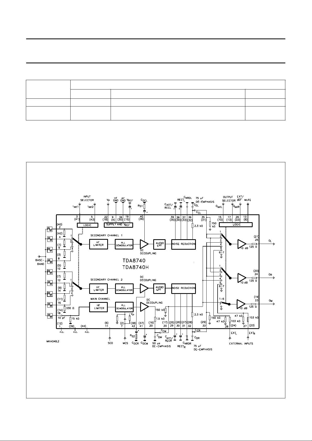
BLOCK DIAGRAM
NAME DESCRIPTION VERSION
(1)
plastic quad flat package; 44 leads (lead length 1.3 mm);
body 10 × 10 × 1.75 mm
PACKAGE
“Quality Reference Handbook”
SOT307-2
The pin numbers in parenthesis refer to the QFP44 package.
Fig.1 Block diagram.
October 1994 3
Page 4

Philips Semiconductors Product specification
Satellite sound circuit with noise reduction TDA8740; TDA8740H
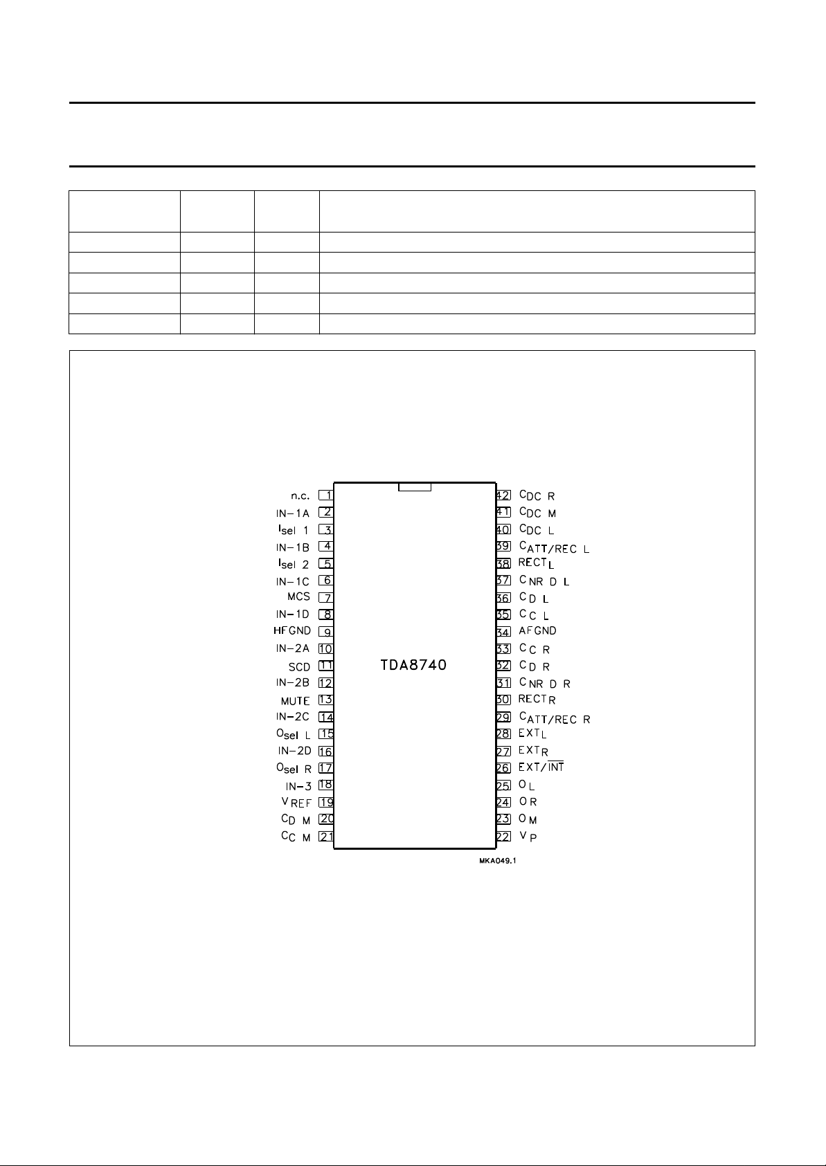
PINNING
SYMBOL
PIN
SDIP42
PIN
QFP44
DESCRIPTION
n.c. 1 39 not connected
IN-1A 2 40 intercarrier input A for Channel 1 (left)
I
sel 1
3 41 input select switch bit 1
IN-1B 4 42 intercarrier input B for Channel 1 (left)
I
sel 2
5 43 input select switch bit 2
IN-1C 6 1 intercarrier input C for Channel 1 (left)
MCS 7 2 main channel PLL lock-in range select/disable
IN-1D 8 3 intercarrier input D for Channel 1 (left)
HFGND 9 4 ground for HF section
IN-2A 10 5 intercarrier input A for Channel 2 (right)
SCD 11 6 secondary channels PLLs disable
IN-2B 12 7 intercarrier input B for Channel 2 (right)
MUTE 13 8 mute switch
IN-2C 14 9 intercarrier input C for Channel 2 (right)
O
sel L
15 10 output select switch bit 1 (left)
IN-2D 16 11 intercarrier input D for Channel 2 (right)
O
sel R
17 13 output select switch bit 2 (right)
IN-3 18 14 intercarrier input for main channel
V
REF
C
D M
C
C M
V
P
O
M
O
R
O
L
INT 26 22 output switch bit 3 (external/internal)
EXT/
EXT
R
EXT
L
C
ATT/REC R
RECT
R
C
NR D R
C
D R
C
C R
19 15 decoupling capacitor for reference voltage
20 16 de-emphasis capacitor for main channel
21 17 audio pass-through capacitor input for main channel
22 18 positive supply voltage
23 19 main channel output
24 20 right channel output
25 21 left channel output
27 23 external audio input (right)
28 24 external audio input (left)
29 25 attack/recovery capacitor (right)
30 26 rectifier DC decoupling (right)
31 27 noise reduction de-emphasis capacitor (right)
32 28 fixed de-emphasis capacitor (right)
33 29 audio pass-through capacitor input for right channel
AFGND 34 30 ground for AF section
C
C L
C
D L
C
NR D L
RECT
C
ATT/REC L
L
35 31 audio pass-through capacitor input for left channel
36 32 fixed de-emphasis capacitor (left)
37 33 noise reduction de-emphasis capacitor (left)
38 34 rectifier DC decoupling (left)
39 35 attack/recovery capacitor (left)
October 1994 4
Page 5
Philips Semiconductors Product specification
Satellite sound circuit with noise reduction TDA8740; TDA8740H
C
C
C
DC L
DC M
DC R
SYMBOL
PIN
SDIP42
40 36 DC decoupling capacitor (left)
41 37 DC decoupling capacitor (main)
42 38 DC decoupling capacitor (right)
PIN
QFP44
n.c. − 12 not connected
n.c. − 44 not connected
DESCRIPTION
Fig.2 Pin configuration (SDIP42).
October 1994 5
Page 6
Philips Semiconductors Product specification
Satellite sound circuit with noise reduction TDA8740; TDA8740H
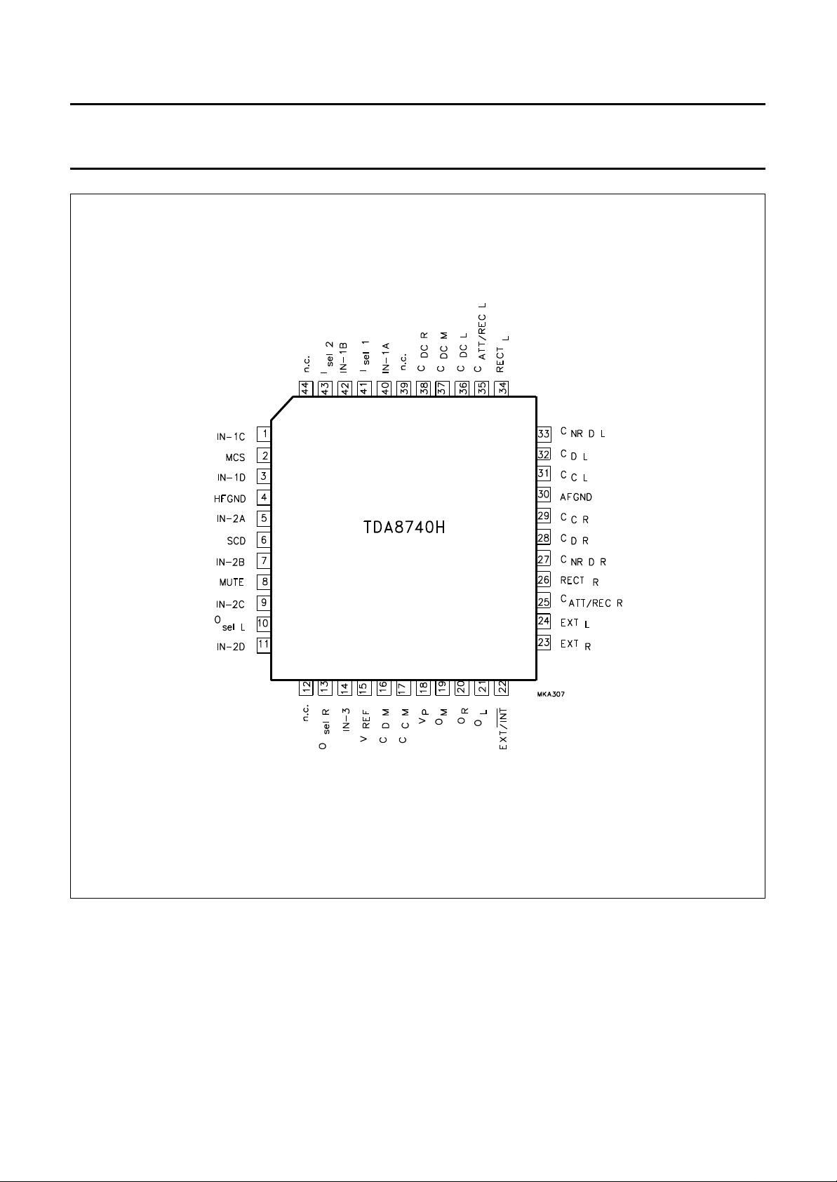
Fig.3 Pin configuration (QFP44).
October 1994 6
Page 7

Philips Semiconductors Product specification
Satellite sound circuit with noise reduction TDA8740; TDA8740H
FUNCTIONAL DESCRIPTION
Satellite sound
The baseband signal coming from a satellite tuner
contains the demodulated video signal plus a number of
sound carriers to facilitate reception of a
PAL/NTSC/SECAM satellite signal.
Nearest to the video signal is the main sound carrier which
carries the single channel sound related to the video. This
is an FM modulated carrier with a fixed pre-emphasis. The
carrier frequency can be in the range of 5.8 to 6.8 MHz.
Additionally, a number of optional secondary sound
carriers may be present which can be used for stereo or
multi-language sound related to the video, or for unrelated
radio sound. These carriers are also FM modulated, but for
better sound quality (improved signal-to-noise
performance) broadcast satellites (e.g. ‘ASTRA’) use a
noise reduction system (adaptive pre-emphasis circuit,
combined with a fixed pre-emphasis).
These secondary carrier frequencies can be in the range
of 6.30 to 8.28 MHz. The TDA8740; H contains all circuitry
for processing the main channel and for two secondary
channels, from baseband signal to line (SCART) output
drivers. The desired frequencies can be routed to the
TDA8740; H via bandpass filters.
Main channel (see Fig.1)
The lock-in range of the main channel PLL can be
switched between 5.5 to 7.5 MHz, PLL off and 10.0 to
11.5 MHz using the MCS signal at pin 7 (2) [when pin 7 (2)
is at logic 0, being a voltage from 0 to 1.2 V, the lock-in
range = 5.5 to 7.5 MHz; when pin 7 (2) is at logic 1, being
a voltage from 3.5 V until V
11.5 MHz; when pin 7 (2) is in the mid voltage position,
being a voltage from 1.8 to 2.8 V, the main channel PLL is
switched off]. The mid voltage position of the MCS pin can
also be obtained by a floating MCS pin if the circuit supply
voltage Vp is 10.8 to 13.2 V. The voltage on the MCS pin
is then determined by the resistor divider at this pin
between VP and ground.
If only one fixed carrier frequency for the main channel is
to be demodulated (e.g. 6.5 MHz), the lock-in range of the
PLL should be switched to 5.5 to 7.5 MHz. The baseband
signal is applied to the main channel input, pin 18 (14) via
a 6.5 MHz ceramic bandpass filter. Alternatively, if there is
a requirement to demodulate different main channel
frequencies, these frequencies can be transferred to a
fixed intermediate frequency (e.g. 10.7 MHz) using an
external mixer and oscillator-frequency synthesizer. In this
event the lock-in range of the PLL should be switched to
, the lock-in range = 10.0 to
P
10.0 to 11.5 MHz. The IF signal is applied to the main
channel input, pin 18 (14) via a 10.7 MHz ceramic
bandpass filter.
The filtered signal is AC-coupled to a limiter/amplifier and
then to a PLL demodulator. The PLL FM demodulator
ensures that the demodulator is alignment-free. High gain
and DC error signals from the PLL, which are
superimposed on the demodulator output, require DC
decoupling. A buffer amplifier is used to amplify the signal
to the same level as the secondary channels and
decouples DC using an electrolytic capacitor connected to
pin 41 (37). The demodulator output signal is fed to pin 20
(16) via an internal resistor. The output signal can be
de-emphasized by means of this resistor and an external
capacitor connected to ground.
Capacitor value = de-emphasis time constant per 1500
(for 50 µs: 33 nF).
From here the signal is fed to the output selectors. The
signal is amplified to 500 mV(RMS) (i.e. −6 dBV) in the
output amplifiers.
Secondary channels
Up to eight secondary channel inputs are available at pins
2, 4, 6, 8, 10, 12, 14 and 16 (1, 3, 5, 7, 9, 11, 40 and 42).
External ceramic bandpass filters tuned to the required
secondary sound carrier frequencies route these signals to
the inputs.
For stereo applications the TDA8740; TDA8740H contains
two identical secondary sound processing channels. For
each channel it is possible to select from four inputs (IN-A,
IN-B, IN-C and IN-D) using the input selector (see Logic
Table 1). With the input switch several stereo signals or
languages can be selected for demodulation. It should be
noted that the inputs are identical and can be freely
interchanged. Secondary Channel 1 will also be referred
to as ‘LEFT’ or ‘LANGUAGE 1’ and secondary Channel 2
will also be referred to as ‘RIGHT’ or ‘LANGUAGE 2’.
From the input selector switch the signals are coupled to
limiter/amplifiers and then to the PLL demodulators.
Processing is similar to the main channel. The
demodulator output signal is amplified in a buffer amplifier
and DC decoupled using electrolytic capacitors connected
to pins 40 (36) (left) and 42 (38) (right). The output level is
set with a 220 Ω resistor connected in series with the
capacitor.
High frequency components in the amplified PLL output
signal are filtered out in the audio LPF block (4th order
Butterworth low-pass filter) to prevent unwanted influence
on the noise reduction.
October 1994 7
Page 8

Philips Semiconductors Product specification
Satellite sound circuit with noise reduction TDA8740; TDA8740H
NOISE REDUCTION (NR)
The noise reduction can be regarded as an input
level-dependent low-pass filter (adaptive de-emphasis
system) followed by a fixed de-emphasis. With maximum
input level (0 dB) the frequency response of the first part
(i.e. without the fixed de-emphasis) is virtually flat. As the
input level is lowered by x-dB, the higher output
frequencies will be reduced an extra x-dB with respect to
the lower frequencies (1 : 2 expansion).
The NR output signal is fed to pin 36 (32) (left) and pin 32
(28) (right) via internal resistors.
Fixed de-emphasis is achieved by these resistors and
external capacitors connected to ground. The signals are
DC decoupled via pins 36/35 (32/31) and 32/33 (28/29)
and then routed to the output selectors.
UTPUT SELECTION
O
With the output selector (see Table 2) the outputs at
pins 25 and 24 (21 and 20) can be switched to the different
channels. Both outputs can be switched to both secondary
channels, to the main channel and to the external inputs at
pin 28 and 27 (24 and 23) for IC chaining purposes.
Pin 23 (19) is a separate output which delivers the main
channel only, thereby creating the possibility of having
three different output channels simultaneously e.g. for use
in hi-fi VCRs.
ABBREVIATIONS
= modulating frequency.
f
MOD
∆fM = frequency deviation of the main Channel.
∆fS1 = frequency deviation of secondary Channel 1 (left).
∆fS2 = frequency deviation of secondary Channel 2 (right).
fOM = carrier frequency of main Channel.
f
= carrier frequency of secondary Channel 1.
OS1
f
= carrier frequency of secondary Channel 2.
OS2
LPF = Low-Pass Filter.
NR = Noise Reduction.
PLL = Phase-Locked-Loop
The outputs at pins 25 and 24 (21 and 20) can be muted
by setting the MUTE signal at pin 13 (8) to logic 1 (switch
positions 6 and 7).
The output at pin 23 (19) can be muted by setting the
MUTE signal and the EXT/INT signal at pin 26 (22) both
logic 1 (switch position 7).
All outputs at pins 23, 24 and 25 (19, 20 and 21) are line
drivers with SCART level capability and are short-circuit
protected by 125 Ω output resistors.
Output level of all channels = −6 dBV typical when
frequency deviation of FM signal is 54% of maximum
frequency deviation (i.e. 0.54 × 85 kHz = 46 kHz for the
main channel and 0.54 × 50 kHz = 27 kHz for the
secondary channels) at 1 kHz modulation frequency
(reference level).
October 1994 8
Page 9

Philips Semiconductors Product specification
Satellite sound circuit with noise reduction TDA8740; TDA8740H
LIMITING VALUES
In accordance with the Absolute Maximum Rating System (IEC 134).
SYMBOL PARAMETER CONDITIONS MIN. MAX. UNIT
V
P
V
n
V
n
V
n
T
stg
T
amb
Notes
1. All voltages referenced to ground pins 9 and 34 (4 and 30).
2. All voltages referenced to ground pins 9 and 34 (4 and 30). These voltages must not exceed V
at any time.
supply voltage note 1 0 13.2 V
voltage on pins 2, 4, 6, 8, 10, 12, 14 and 16
note 2 0 1 V
(1, 3, 5, 7, 9, 11, 40 and 42)
voltage on pins 3, 5, 1 1, 13, 15, 17, 20, 21, 23 to 26, 31, 33,
note 2 0 9 V
35, 37, 40, 41, and 42 (6, 8, 10, 13, 16, 17, 19, 20 to 22, 27,
29, 31, 33, 36, 37, 38, 41 and 43)
voltage on pins 7, 18, 19, 27 to 30, 32, 36, 38 and 39
note 1 0 V
V
P
(2, 14, 15, 23 to 26, 28, 32, 34 and 35)
storage temperature −55 +150 °C
operating ambient temperature −20 +70 °C
or maximum value
P
THERMAL CHARACTERISTICS
SYMBOL PARAMETER VALUE UNIT
R
th j-a
thermal resistance from junction to ambient in free air
SDIP42 53 K/W
QFP44 69 K/W
DC CHARACTERISTICS
All voltages referenced to ground at pins 9 and 34 (4 and 30). Measured in test circuit Fig.4; V
∆fM= ∆fS1= ∆fS2= 0 kHz (no modulation); fOM= 6.5 MHz; f
= 7.02 MHz; f
OS1
= 7.20 MHz; HF level at pin 18 (14):
OS2
=12V; T
P
amb
=25°C;
40 mV (RMS); HF level at selected secondary inputs: 20 mV (RMS); MCS = logic 0 [V7(V2)=0V];
SCD = logic 0 [V11(V6) = 0 V]; unless otherwise specified.
SYMBOL PARAMETER MIN. TYP. MAX. UNIT
V
P
I
P
P
tot
V
n
supply voltage 8.0 12 13.2 V
supply current − 38 45 mA
total power dissipation −−600 mW
voltage on pins 20, 21, 23, 24, 25, 27, 28, 30, 32, 33, 35, 36
− 3.8 − V
and 38 (16, 17, 19, 20, 21, 23, 24, 26, 28, 29, 31, 32 and 34)
V
V
REF
n
input reference voltage on pin 19 (15) 3.7 3.8 3.9 V
voltage on pins 2, 4, 6, 8, 10, 12, 14 and 16
− 0 − V
(1, 3, 5, 7, 9, 11, 40 and 42)
V
CDCL,CDCR
V
CDCM
I
IN3
voltage on pins 40 and 42 (36 and 38) − 2.7 − V
voltage on pin 41 (37) − 2.8 − V
input current at pin 18 (14) −−1µA
October 1994 9
Page 10

Philips Semiconductors Product specification
Satellite sound circuit with noise reduction TDA8740; TDA8740H
AC CHARACTERISTICS
All voltages referenced to ground at pins 9 and 34 (4 and 30). Measured in test circuit Fig.4; VP= 12 V; T
f
= 1 kHz; fOM= 6.5 MHz; ∆fM= 46 kHz; ∆fS1= ∆fS2= 27 kHz (reference levels); f
MOD
= 7.02 MHz; f
OS1
HF level at pin 18 (14): 40 mV (RMS); HF level at selected secondary inputs: 20 mV (RMS); MCS = logic 0
[V7(V2) = 0 V]; SCD = logic 0 [V11(V6) = 0 V]; unless otherwise specified.
SYMBOL PARAMETER CONDITIONS MIN. TYP. MAX. UNIT
Main channel - HF input pin 18 (14) and limiter
V
IN3(rms)
V
IN3(rms)
R
IN3
input sensitivity (RMS value) S/N(A) = 40 dB − 1.0 2.0 mV
input signal level (RMS value) −−200 mV
input resistance − 15 − kΩ
Main channel - PLL FM demodulator and DC decoupling amplifier
f
CCO
free-running frequency − 6.5 − MHz
MCS = logic 1 − 10.7 − MHz
∆f
OM
lock range of PLL note 1 5.5 − 7.5 MHz
MCS = logic 1; note 1 10.0 − 11.5 MHz
R
CDM
output resistance for 50 µs
1.24 1.5 1.7 kΩ
de-emphasis pin 20 (16)
V
∆V
CDM
CDM
output voltage pin 20 (16) −18.5 −16.0 −14.5 dBV
spread of PLL output voltage
−−±1dB
over lock range pin 20 (16)
R
CCM
input resistance of output
95 150 200 kΩ
amplifier pin 21 (17)
amb
= 7.20 MHz;
OS2
=25°C;
Main channel - overall performance (output selector in position 4)
V
OM,OR,OL
output voltage pins 23, 24 and
all PLLs locked −9 −6 −4 dBV
25 (19, 20 and 21)
UBM output voltage unbalance pins
23, 24, 25 (19, 20, 21)
output selector in
position 4
−0.5 − +0.5 dB
THD total harmonic distortion all PLLs locked − 0.1 0.5 %
S/N(A) signal-to-noise ratio A-weighted; all PLLs
62 70 − dB
locked
V
OM 15 kHz()
-------------------------------
V
OM 1 kHz()
R
OM,OR,OL
15 kHz frequency response
with respect to 1 kHz pin 23
(19)
output resistance pins 23, 24
no de-emphasis
connected
−0.5 0 +0.5 dB
92 125 150 Ω
and 25 (19, 20 and 21)
α
S/M
crosstalk attenuation from
note 2 − 74 − dB
secondary channels to main
MUTE
att
mute attenuation output selector in
74 −−dB
position 7
SVRR supply voltage ripple rejection V
= 100 mV; fi=70Hz − 35 − dB
RR
October 1994 10
Page 11

Philips Semiconductors Product specification
Satellite sound circuit with noise reduction TDA8740; TDA8740H
SYMBOL PARAMETER CONDITIONS MIN. TYP. MAX. UNIT
Secondary channels 1 and 2 - HF inputs pins 2, 4, 6, 8, 10, 12, 14 and 16 (1, 3, 5, 7, 9, 11, 40 and 42) and
limiters
V
IN1,IN2
V
I(rms)
R
i
Secondary channels 1 and 2 - PLL FM demodulators (input selector in position 1)
f
CCO1
f
CCO2
∆f
OS1/2
R
S1,S2
V
CDCL,CDCR (rms
∆V
CDCL,CDCR
) PLL output voltage pins 40
input sensitivity (RMS value) S/N(A) = 40 dB − 0.8 1.5 mV
input signal level (RMS value) −−200 mV
input resistance 260 330 380 Ω
free running frequency PLL1 − 7.0 − MHz
free running frequency PLL2 − 7.2 − MHz
lock range of PLLs note 3 6.0 − 8.5 MHz
series resistance for optimum
0 0.22 1.0 kΩ
frequency response
adjustment
pins to be left open-circuit − 7 − mV
and 42 (36 and 38) (RMS
value)
spread of PLL output voltage
−−±1dB
over lock range
Secondary channels - overall performance of LPF and NR (input and output selectors in position 1)
R
o
output resistance for 75 µs
1.9 2.3 2.6 kΩ
de-emphasis pins 36 and 32
(32 and 28)
R
i
input resistance of output
95 150 200 kΩ
amplifiers pins 35 and 33
(31 and 29)
V
OL,OR
output voltage level
note 4 −8 −6 −4 dBV
pins 25 and 24 (21 and 20)
UBS unbalance voltage outputs
note 4 −1 − +1 dBV
pins 25 and 24 (21 and 20)
THD total harmonic distortion note 4 − 0.1 0.5 %
S/N(A) signal-to-noise ratio A-weighted; note 4 72 80 − dB
R
o
output resistance pins 25 and
note 4 92 125 150 Ω
24 (21 and 20)
MUTE
att
mute attenuation output selector in
74 −−dB
position 6; note 4
α
S/S
crosstalk attenuation between
note 5 − 74 − dB
secondary channels
α
M/S
crosstalk attenuation from
note 6 − 74 − dB
main channel to secondary
V
offset(DC)
DC offset voltage on
all PLLs locked; ∆f = 0 14 16 20 mV
attack/recovery capacitors
pins 29, 39 (25, 35)
SVRR supply voltage ripple rejection V
= 100 mV; fi=70Hz − 25 − dB
RR
October 1994 11
Page 12

Philips Semiconductors Product specification
Satellite sound circuit with noise reduction TDA8740; TDA8740H
SYMBOL PARAMETER CONDITIONS MIN. TYP. MAX. UNIT
Secondary channels - low-pass filter pins 38 and 30 (34 and 26)
V
RECTL RECTR 50 kHz(),
---------------------------------------------------------- -
V
RECTL RECTR 1 kHz(),
50 kHz frequency response
with respect to 1 kHz
Secondary channels - noise reduction pins 25 and 24 (21 and 20); note 4
V
OL,OR
output voltage at 0 dB noise
reduction input level
V
OL OR 15 kHz(),
---------------------------------------
V
OL OR 1 kHz(),
V
OL,OR
15 kHz frequency response
with respect to 1 kHz at 0 dB
noise reduction input level
output voltage at −20 dB noise
reduction input level
V
OL OR 15 kHz(),
---------------------------------------
V
OL OR 1 kHz(),
15 kHz frequency response
with respect to 1 kHz at
−20 dB noise reduction input
level
note 7 −25 −16 −9dB
∆fS1= ∆fS2= 50 kHz;
−1+1+3dBV
no fixed de-emphasis
connected
= ∆fS2= 50 kHz;
∆f
S1
−2 0 +2 dB
no fixed de-emphasis
connected
∆fS1= ∆fS2= 5 kHz;
−29 −26 −23 dBV
no fixed de-emphasis
connected
= ∆fS2= 5 kHz;
∆f
S1
−13 −11.5 −10 dB
no fixed de-emphasis
connected
External inputs - pin 28 (24) (left) and pin 27 (23) (right) - overall performance (output selector in position 5)
V
EXTR,EXTL
R
i
V
OL,OR
input signal level −−6 dBV
input resistance 95 150 200 kΩ
output level pins 25 and 24 (21
V
EXTR, EXTL
= −6 dBV −6.5 −6.0 −5.5 dBV
and 20)
THD total harmonic distortion V
EXTR, EXTL
= −6 dBV;
−−0.1 %
fi= 1 kHz
S/N(A) signal-to-noise ratio A-weighted;
V
EXTR, EXTL
α
L/R,αR/L
crosstalk fi= 1 kHz − 80 − dB
= −6 dBV
80 −−dB
Input selector control circuit pins 3 and 5 (41 and 43) (see also T able 1) and secondary channels PLLs disable
[SCD pin 11 (6)]; pins 3, 5 and 11 (41, 43 and 6) left open-circuit = logic HIGH
V
IL
V
IH
R
i
LOW level input voltage 0 − 1.2 V
HIGH level input voltage 3.5 − 9V
input resistance connected to V
P
65 100 130 kΩ
October 1994 12
Page 13

Philips Semiconductors Product specification
Satellite sound circuit with noise reduction TDA8740; TDA8740H
SYMBOL PARAMETER CONDITIONS MIN. TYP. MAX. UNIT
Output selector control circuit (see also T able 2) and main channel PLL lock-in select [MCS pin 7 (2)]; pins 15,
17, 26 and 13 (10, 13, 22 and 8) are MOS inputs and should not be left open-circuit
V
IL
V
IM
V
IMF
V
IH
R
IL
R
IH
I
IL
I
IH
LOW level input voltage limits 0 − 1.2 V
MID level input voltage limits
1.8 − 2.8 V
for MCS pin only
MID level input voltage on
VP must be 10.8 to 13.2 V 17 19 21 %V
MCS pin if MCS pin is floating
HIGH level input voltage limits 3.5 − V
low input resistance MCS pin
12 19 26 kΩ
P
to ground
high input resistance MCS pin
to V
P
LOW level input current
VIL=0V −<−1−µA
52 80 108 kΩ
(not MCS pin)
HIGH level input current
VIH=5V −<1−µA
(not MCS pin)
P
V
Notes
1. At pin 20 (16) the demodulated 1 kHz signal should be present with a typical level of 158 mV (RMS) (−16 dBV), and
THD of maximum 0.5%; VP= 8 to 13.2 V; T
= −20 to +70 °C.
amb
2. Modulation of main channel is OFF; modulation of secondary channels is ON.
3. The electrolytic capacitors at pins 40 and 42 (36 and 38) are removed and 1500 pF capacitors between pin 40 (36)
and ground and between pin 42 (38) and ground are connected. At pins 40 and 42 (36 and 38) the demodulated
1 kHz signals should be present with typical levels of 7 mV (RMS) and THD of maximum 0.5%; VP= 8 to 13.2 V;
T
= −20 to +70 °C.
amb
4. All PLLs locked; RS1=RS2= 220 kΩ.
5. Modulation of secondary channel being measured and main channel is OFF; modulation of other secondary channel
is ON.
6. Modulation of main channel is ON; modulation of secondary channels is OFF.
7. Measured at pins 38 (34) (left) and 30 (26) (right) and no electrolytic capacitors connected to these pins.
October 1994 13
Page 14

Philips Semiconductors Product specification
Satellite sound circuit with noise reduction TDA8740; TDA8740H
Table 1 Truth table for input selection.
SWITCH POSITION STATE PIN 15 (10) PIN 17 (13)
1 pins 2 and 10 (IN-A) (40 and 5) 0 0
2 pins 4 and 12 (IN-B) (42 and 7) 0 1
3 pins 6 and 14 (IN-C) (1 and 9) 1 0
4 pins 8 and 16 (N-D) (3 and 12) 1 1
Table 2 Truth table for output selection (note 1).
SWITCH
POSITION
1 stereo 1 1 0 0
2 left 1 0 0 0
3 right 0 1 0 0
4 main 0 0 0 0
5 external X X 1 0
6 mute secondary X X 0 1
7 mute all X X 1 1
Note
1. X = don’t care.
STATE
PIN 15 (10) PIN 17 (13) PIN 26 (22) PIN 13 (8)
OUTSEL L OUTSEL R EXT/
INT MUTE
October 1994 14
Page 15

Philips Semiconductors Product specification
Satellite sound circuit with noise reduction TDA8740; TDA8740H
Fig.4 Test circuit.
The pin numbers in parenthesis refer to the QFP44 package.
October 1994 15
Page 16

Philips Semiconductors Product specification
Satellite sound circuit with noise reduction TDA8740; TDA8740H
APPLICATION INFORMATION
MCS pin 7 (2) = logic 0; (see Fig.5)
The lock-in range of the main channel PLL is 5.5 to
7.5 MHz. The satellite baseband signal is routed to nine
bandpass filters, eight for the secondary channels and one
for the main channel. For the secondary channels the
bandpass filter terminating resistors are integrated on-chip
(330 Ω typically) so no external resistors are required. For
the main channel this is not the case therefore filters with
different characteristics can be used.
MCS pin 7 (2) = logic 1; (see Fig.6)
The lock-in range of the main channel PLL is now 10.0 to
11.5 MHz. The carrier frequency for the main channel is
transposed to 10.7 MHz by an external frequency
synthesizer and mixer; e.g., if a 6.65 MHz carrier is to be
demodulated this frequency is mixed to 10.7 MHz by
tuning the frequency synthesizer to 17.35 MHz. If the
synthesizer is tuned 17.20 MHz a 6.5 MHz carrier can be
demodulated. In this event the audio output level should
be adjusted to −6 dBV by inserting a 470 Ω resistor in
series with the electrolytic capacitor to pin 41 (37).
If the main channel only is to be demodulated the PLLs of
the secondary channels can be disabled by setting SCD
pin 11 (6) to logic 1.
MCS pin 7 (2) = MID position
The main channel PLL is off if the voltage is between 1.8
and 2.8 V on pin 7 (2). This situation can be obtained by a
floating MCS pin if V
forcing this MCS pin to the desired voltage by an external
voltage source. In that event VP can be in the full range of
8 to 13.2 V. This feature can be used to slightly improve
the signal-to-noise ratio of the secondary channels if the
main channel is not used.
For the main channel the baseband signal is routed to the
mixer, and to eight ceramic bandpass filters for the
secondary channels. For high-end applications the input
level of the NR can be adjusted to give optimal
performance. 0 dB is the maximum input level which
corresponds to the maximum frequency deviation of the
incoming FM signal (50 kHz for secondary channels). If
the NR input signal is too low (HIGH) the NR will attenuate
(favour) the higher audio frequencies too much due to the
expansion character. In general a 1 dB error in the NR
input level will give a 1 dB difference between
LOW (50 Hz) and HIGH (15 kHz) audio frequencies. With
RS1 (RS2) the input level and so the frequency response of
the NR can be adjusted: at 0 dB input level (which
corresponds to a frequency deviation of 50 kHz) the output
level of a 15 kHz modulated signal should be 0.25 dB
lower than that of a 50 Hz modulated signal.
is between 10.8 and 13.2 V or by
P
October 1994 16
Page 17

Philips Semiconductors Product specification
Satellite sound circuit with noise reduction TDA8740; TDA8740H
October 1994 17
Fig.5 Application diagram; MCS = logic 0.
The pin numbers in parenthesis refer to the QFP44 package.
Page 18

Philips Semiconductors Product specification
Satellite sound circuit with noise reduction TDA8740; TDA8740H
October 1994 18
Fig.6 Application diagram; MCS = logic 1.
The pin numbers in parenthesis refer to the QFP44 package.
Page 19

Philips Semiconductors Product specification
Satellite sound circuit with noise reduction TDA8740; TDA8740H
PACKAGE OUTLINES
handbook, full pagewidth
seating plane
3.2
2.9
1.73
max
42
1
39.0
38.4
1.778
(40x)
1.3 max
0.53
max
22
21
0.51
min
14.1
13.7
0.18
4.57
max
15.80
15.24
5.08
max
M
0.32 max
15.24
17.15
15.90
MSA268 - 1
Dimensions in mm.
Fig.7 Plastic shrink dual in-line package; 42 leads (600 mil); SDIP42; SOT270-1.
October 1994 19
Page 20

Philips Semiconductors Product specification
Satellite sound circuit with noise reduction TDA8740; TDA8740H
handbook, full pagewidth
seating
plane
0.1 S
12.9
12.3
44
1
pin 1 index
11
12
34
22
S
1.2
(4x)
0.8
33
0.8
0.40
23
0.20
B
10.1
9.9
12.9
12.3
B
0.15 M
1.2
0.25
0.05
0.8
(4x)
A
detail X
0.95
0.55
0.85
0.75
X
0.25
0.14
0 to 10
2.10
1.70
o
Dimensions in mm.
0.8
0.40
0.20
0.15 M A
10.1
9.9
1.85
1.65
MBB944 - 2
Fig.8 Plastic quad flat package; 44 leads (lead length 1.3 mm); body 10 × 10 × 1.75 mm (QFP44; SOT307-2).
October 1994 20
Page 21

Philips Semiconductors Product specification
Satellite sound circuit with noise reduction TDA8740; TDA8740H
SOLDERING
Plastic dual in-line packages
BY DIP OR WAVE
The maximum permissible temperature of the solder is
260 °C; this temperature must not be in contact with the
joint for more than 5 s. The total contact time of successive
solder waves must not exceed 5 s.
The device may be mounted up to the seating plane, but
the temperature of the plastic body must not exceed the
specified storage maximum. If the printed-circuit board has
been pre-heated, forced cooling may be necessary
immediately after soldering to keep the temperature within
the permissible limit.
EPAIRING SOLDERED JOINTS
R
Apply the soldering iron below the seating plane (or not
more than 2 mm above it). If its temperature is below
300 °C, it must not be in contact for more than 10 s; if
between 300 and 400 °C, for not more than 5 s.
Quad flat-packs
YWAVE
B
During placement and before soldering, the component
must be fixed with a droplet of adhesive. After curing the
adhesive, the component can be soldered. The adhesive
can be applied by screen printing, pin transfer or syringe
dispensing.
BY SOLDER PASTE REFLOW
Reflow soldering requires the solder paste (a suspension
of fine solder particles, flux and binding agent) to be
applied to the substrate by screen printing, stencilling or
pressure-syringe dispensing before device placement.
Several techniques exist for reflowing; for example,
thermal conduction by heated belt, infrared, and
vapour-phase reflow. Dwell times vary between 50 and
300 s according to method. Typical reflow temperatures
range from 215 to 250 °C.
Preheating is necessary to dry the paste and evaporate
the binding agent. Preheating duration: 45 min. at 45 °C.
EPAIRING SOLDERED JOINTS (BY HAND-HELD SOLDERING
R
IRON OR PULSE
-HEATED SOLDER TOOL)
Fix the component by first soldering two, diagonally
opposite, end pins. Apply the heating tool to the flat part of
the pin only. Contact time must be limited to 10 s at up to
300 °C. When using proper tools, all other pins can be
soldered in one operation within 2 to 5 s at between 270
and 320 °C. (Pulse-heated soldering is not recommended
for SO packages.)
For pulse-heated solder tool (resistance) soldering of VSO
packages, solder is applied to the substrate by dipping or
by an extra thick tin/lead plating before package
placement.
Maximum permissible solder temperature is 260° C and
maximum duration of package immersion in solder bath is
10 s, if allowed to cool to less than 150 °C within 6 s.
Typical dwell time is 4 s at 250 °C.
A modified wave soldering technique is recommended
using two solder waves (dual-wave), in which, in a
turbulent wave with high-upward pressure is followed by a
smooth laminar wave. Using a mildly-activated flux
eliminates the need for removal of corrosive residues in
most applications.
October 1994 21
Page 22

Philips Semiconductors Product specification
Satellite sound circuit with noise reduction TDA8740; TDA8740H
DEFINITIONS
Data sheet status
Objective specification This data sheet contains target or goal specifications for product development.
Preliminary specification This data sheet contains preliminary data; supplementary data may be published later.
Product specification This data sheet contains final product specifications.
Limiting values
Limiting values given are in accordance with the Absolute Maximum Rating System (IEC 134). Stress above one or
more of the limiting values may cause permanent damage to the device. These are stress ratings only and operation
of the device at these or at any other conditions above those given in the Characteristics sections of the specification
is not implied. Exposure to limiting values for extended periods may affect device reliability.
Application information
Where application information is given, it is advisory and does not form part of the specification.
LIFE SUPPORT APPLICATIONS
These products are not designed for use in life support appliances, devices, or systems where malfunction of these
products can reasonably be expected to result in personal injury. Philips customers using or selling these products for
use in such applications do so at their own risk and agree to fully indemnify Philips for any damages resulting from such
improper use or sale.
October 1994 22
Page 23

Philips Semiconductors Product specification
Satellite sound circuit with noise reduction TDA8740; TDA8740H
NOTES
October 1994 23
Page 24

Philips Semiconductors – a worldwide company
Argentina: IEROD, Av. Juramento 1992 - 14.b, (1428)
BUENOS AIRES, Tel. (541)786 7633, Fax. (541)786 9367
Australia: 34 Waterloo Road, NORTH RYDE, NSW 2113,
Tel. (02)805 4455, Fax. (02)805 4466
Austria: Triester Str. 64, A-1101 WIEN, P.O. Box 213,
Tel. (01)60 101-1236, Fax. (01)60 101-1211
Belgium: Postbus 90050, 5600 PB EINDHOVEN, The Netherlands,
Tel. (31)40 783 749, Fax. (31)40 788 399
Brazil: Rua do Rocio 220 - 5
CEP: 04552-903-SÃO PAULO-SP, Brazil.
P.O. Box 7383 (01064-970).
Tel. (011)821-2333, Fax. (011)829-1849
Canada: PHILIPS SEMICONDUCTORS/COMPONENTS:
Tel. (800) 234-7381, Fax. (708) 296-8556
Chile: Av. Santa Maria 0760, SANTIAGO,
Tel. (02)773 816, Fax. (02)777 6730
Colombia: IPRELENSO LTDA, Carrera 21 No. 56-17,
77621 BOGOTA, Tel. (571)249 7624/(571)217 4609,
Fax. (571)217 4549
Denmark: Prags Boulevard 80, PB 1919, DK-2300 COPENHAGEN S,
Tel. (032)88 2636, Fax. (031)57 1949
Finland: Sinikalliontie 3, FIN-02630 ESPOO,
Tel. (9)0-50261, Fax. (9)0-520971
France: 4 Rue du Port-aux-Vins, BP317,
92156 SURESNES Cedex,
Tel. (01)4099 6161, Fax. (01)4099 6427
Germany: P.O. Box 10 63 23, 20043 HAMBURG,
Tel. (040)3296-0, Fax. (040)3296 213.
Greece: No. 15, 25th March Street, GR 17778 TAVROS,
Tel. (01)4894 339/4894 911, Fax. (01)4814 240
Hong Kong: PHILIPS HONG KONG Ltd., 6/F Philips Ind. Bldg.,
24-28 Kung Yip St., KWAI CHUNG, N.T.,
Tel. (852)424 5121, Fax. (852)428 6729
India: Philips INDIA Ltd, Shivsagar Estate, A Block ,
Dr. Annie Besant Rd. Worli, Bombay 400 018
Tel. (022)4938 541, Fax. (022)4938 722
Indonesia: Philips House, Jalan H.R. Rasuna Said Kav. 3-4,
P.O. Box 4252, JAKARTA 12950,
Tel. (021)5201 122, Fax. (021)5205 189
Ireland: Newstead, Clonskeagh, DUBLIN 14,
Tel. (01)640 000, Fax. (01)640 200
Italy: PHILIPS SEMICONDUCTORS S.r.l.,
Piazza IV Novembre 3, 20124 MILANO,
Tel. (0039)2 6752 2531, Fax. (0039)2 6752 2557
Japan: Philips Bldg13-37, Kohnan 2-chome, Minato-ku, TOKYO 108,
Tel. (03)3740 5028, Fax. (03)3740 0580
Korea: (Republic of) Philips House, 260-199 Itaewon-dong,
Yongsan-ku, SEOUL, Tel. (02)794-5011, Fax. (02)798-8022
Malaysia: No. 76 Jalan Universiti, 46200 PETALING JAYA,
SELANGOR, Tel. (03)750 5214, Fax. (03)757 4880
Mexico: 5900 Gateway East, Suite 200, EL PASO, TX 79905,
Tel. 9-5(800)234-7381, Fax. (708)296-8556
Netherlands: Postbus 90050, 5600 PB EINDHOVEN, Bldg. VB
Tel. (040)783749, Fax. (040)788399
New Zealand: 2 Wagener Place, C.P.O. Box 1041, AUCKLAND,
Tel. (09)849-4160, Fax. (09)849-7811
Norway: Box 1, Manglerud 0612, OSLO,
Tel. (022)74 8000, Fax. (022)74 8341
th
floor, Suite 51,
Pakistan: Philips Electrical Industries of Pakistan Ltd.,
Exchange Bldg. ST-2/A, Block 9, KDA Scheme 5, Clifton,
KARACHI 75600, Tel. (021)587 4641-49,
Fax. (021)577035/5874546.
Philippines: PHILIPS SEMICONDUCTORS PHILIPPINES Inc,
106 Valero St. Salcedo Village, P.O. Box 2108 MCC, MAKATI,
Metro MANILA, Tel. (02)810 0161, Fax. (02)817 3474
Portugal: PHILIPS PORTUGUESA, S.A.,
Rua dr. António Loureiro Borges 5, Arquiparque - Miraflores,
Apartado 300, 2795 LINDA-A-VELHA,
Tel. (01)4163160/4163333, Fax. (01)4163174/4163366.
Singapore: Lorong 1, Toa Payoh, SINGAPORE 1231,
Tel. (65)350 2000, Fax. (65)251 6500
South Africa: S.A. PHILIPS Pty Ltd.,
195-215 Main Road Martindale, 2092 JOHANNESBURG,
P.O. Box 7430 Johannesburg 2000,
Tel. (011)470-5911, Fax. (011)470-5494.
Spain: Balmes 22, 08007 BARCELONA,
Tel. (03)301 6312, Fax. (03)301 42 43
Sweden: Kottbygatan 7, Akalla. S-164 85 STOCKHOLM,
Tel. (0)8-632 2000, Fax. (0)8-632 2745
Switzerland: Allmendstrasse 140, CH-8027 ZÜRICH,
Tel. (01)488 2211, Fax. (01)481 77 30
Taiwan: PHILIPS TAIWAN Ltd., 23-30F, 66, Chung Hsiao West
Road, Sec. 1. Taipeh, Taiwan ROC, P.O. Box 22978,
TAIPEI 100, Tel. (02)388 7666, Fax. (02)382 4382.
Thailand: PHILIPS ELECTRONICS (THAILAND) Ltd.,
209/2 Sanpavuth-Bangna Road Prakanong,
Bangkok 10260, THAILAND,
Tel. (662)398-0141, Fax. (662)398-3319.
Turkey:Talatpasa Cad. No. 5, 80640 GÜLTEPE/ISTANBUL,
Tel. (0212)279 2770, Fax. (0212)269 3094
United Kingdom: Philips Semiconductors LTD.,
276 Bath road, Hayes, MIDDLESEX UB3 5BX,
Tel. (081)73050000, Fax. (081)7548421
United States:811 East Arques Avenue, SUNNYVALE,
CA 94088-3409, Tel. (800)234-7381, Fax. (708)296-8556
Uruguay: Coronel Mora 433, MONTEVIDEO,
Tel. (02)70-4044, Fax. (02)92 0601
For all other countries apply to: Philips Semiconductors,
International Marketing and Sales, Building BE-p,
P.O. Box 218, 5600 MD, EINDHOVEN, The Netherlands,
Telex 35000 phtcnl, Fax. +31-40-724825
SCD35 © Philips Electronics N.V. 1994
All rights are reserved. Reproduction in whole or in part is prohibited without the
prior written consent of the copyright owner.
The information presented in this document does not form part of any quotation
or contract, is believed to be accurate and reliable and may be changed without
notice. No liability will be accepted by the publisher for any consequence of its
use. Publication thereof does not convey nor imply any license under patent- or
other industrial or intellectual property rights.
Printed in The Netherlands
533061/1500/02/pp24 Date of release: October 1994
Document order number: 9397 740 60011
Philips Semiconductors
 Loading...