

Page 1

INTEGRATED CIRCUITS
DATA SH EET
TDA8735
PLL frequency synthesizer
Product specification
File under Integrated Circuits, IC01
Philips Semiconductors
September 1994
Page 2
Philips Semiconductors Product specification
PLL frequency synthesizer TDA8735
FEATURES
• Complete 30 MHz single-chip tuning system
• Loop amplifier included
• 2-level current amplifier (charge pump) for adjusting the
loop gain
• A powerful digital memory phase detector
• Programmable reference frequencies of 1 kHz, 10 kHz
or 25 kHz
• I2C-bus interface
• Programmable address select input
• Software controlled switch output.
APPLICATIONS
• Satellite sound receiver
• Radio receiver: LW, MW and SW.
GENERAL DESCRIPTION
The TDA8735 is a single-chip PLL synthesizer designed
for satellite receivers. The device can be set to two
different addresses which can be used in applications
where independently tuned VCOs are required.
To adapt to different frequency accuracy, 3 reference
frequencies are selectable via the I2C-bus. The charge
pump current can be set to 2 values with a ratio of 1 : 100
via the I2C-bus.
A programmable switch (open collector) is integrated to
enable mode or normal switching, or other types of
application.
QUICK REFERENCE DATA
SYMBOL PARAMETER CONDITIONS MIN. TYP. MAX. UNIT
V
CC1
V
CC2
I
CC1
I
CC2
f
i(max)
f
i(min)
V
i(rms)
P
tot
T
amb
supply voltage (pin 3) 4.5 5.0 5.5 V
supply voltage (pin 16) V
CC1
8.5 12 V
supply current (pin 3) outputs unloaded 12 20 28 mA
supply current (pin 16) outputs unloaded 0.2 0.5 1 mA
maximum input frequency 30 −−MHz
minimum input frequency −−512 kHz
input voltage (RMS value) 30 − 500 mV
total power dissipation − 0.14 − W
operating ambient temperature −30 − +85 °C
ORDERING INFORMATION
TYPE
NUMBER
NAME DESCRIPTION VERSION
PACKAGE
TDA8735 DIP16 plastic dual in-line package; 16 leads (300 mil) SOT38-1
TDA8735T SO16 plastic small outline package; 16 leads; body width 3.9 mm SOT109-1
September 1994 2
Page 3
Philips Semiconductors Product specification
PLL frequency synthesizer TDA8735
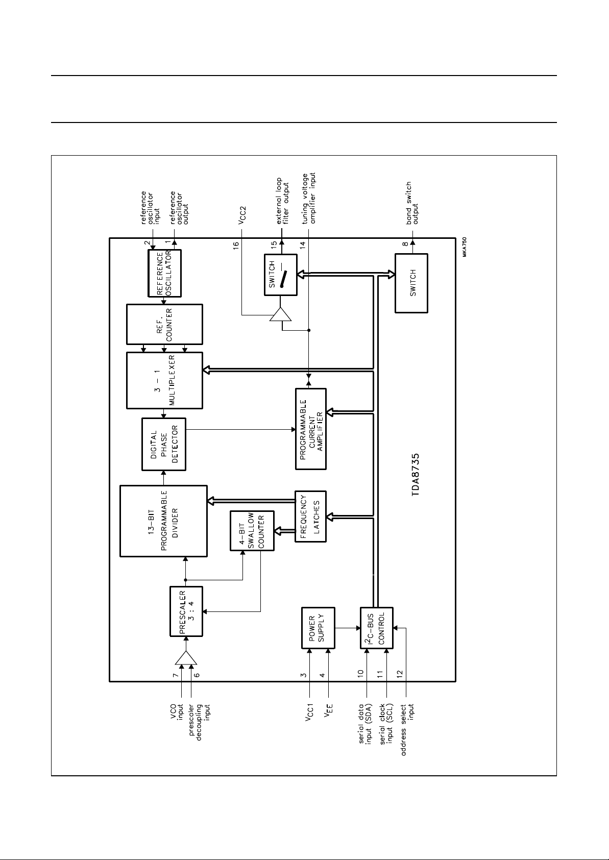
BLOCK DIAGRAM
September 1994 3
Fig.1 Block diagram.
Page 4
Philips Semiconductors Product specification
PLL frequency synthesizer TDA8735
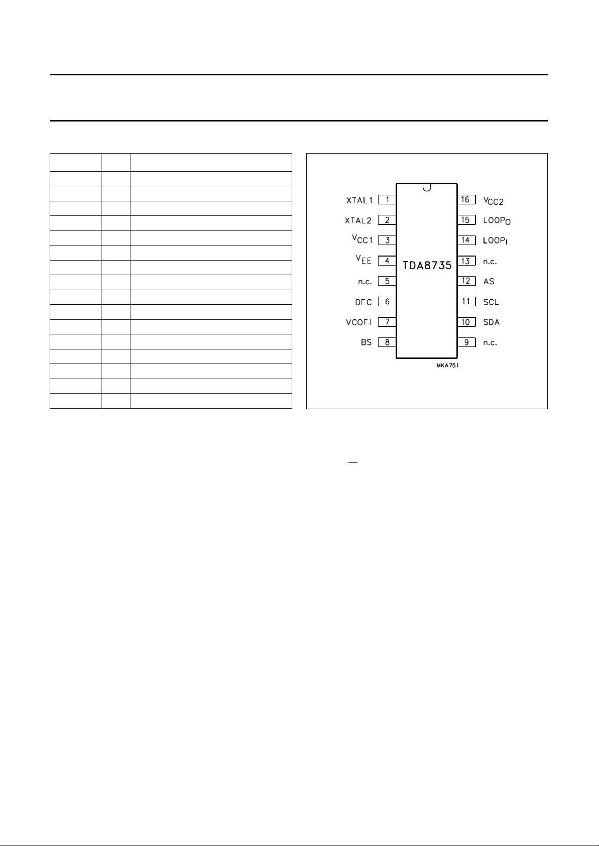
PINNING
SYMBOL PIN DESCRIPTION
XTAL1 1 reference oscillator output
XTAL2 2 reference oscillator input
V
CC1
V
EE
n.c. 5 not connected
DEC 6 prescaler decoupling
VCOFI 7 VCO input frequency
BS 8 band switch output
n.c. 9 not connected
SDA 10 serial data input (I
SCL 11 serial clock input (I
AS 12 address select input (I
n.c. 13 not connected
LOOP
I
LOOP
O
V
CC2
3 supply voltage 1
4 ground
2
C-bus)
2
C-bus)
2
C-bus)
14 tuning voltage amplifier input
15 external loop filter output
16 supply voltage 2
Fig.2 Pin configuration.
FUNCTIONAL DESCRIPTION
The TDA8735 contains the following parts and facilities:
• Input amplifier VCO-signal.
• A prescaler with the divisors 3 : 4 and a 2-bit
programmable swallow counter.
• A 13-bit programmable counter.
• A digital memory phase detector.
• A reference frequency channel comprised of a 4 MHz
crystal oscillator followed by a reference counter; the
reference frequency can be 1 kHz, 10 kHz or 25 kHz
and is applied to the digital memory phase detector.
2
C-bus interface with data latches and control logic;
• An I
the I2C-bus is intended for communication between
microcontrollers and different ICs or modules. Detailed
information on the I2C-bus specification is available on
request.
• A software-controlled switch output.
• A programmable current amplifier (charge pump) which
consists of a 5 µA and a 500 µA current source, this
allows adjustment of loop gain, thus providing
high-current high-speed tuning and low current-stable
tuning. The output at the loop amplifier can deliver a
tuning voltage of up to 10.5 V (V
CC2
− 1.5 V).
Controls
The TDA8735 is controlled via the 2-wire I
2
C-bus. As slave
receiver for programming there is one module address, a
logic 0 (R/W bit), a subaddress byte and four data bytes.
The subaddress determines which one of the four data
bytes is transmitted first. The module address contains a
programmable address bit (D1) which with address select
input AS (pin 12) makes it possible to operate two
TDA8735 in one system.
The auto increment facility of the I2C-bus allows
programming of the TDA8735 within one transmission
(address + subaddress + 4 data bytes).
The TDA8735 can also be partially programmed.
Transmission must then be ended by a stop condition.
The bit organization of the 4 data bytes is illustrated in
Fig.3 and is described below.
The divider number is defined by 15-bit words, bits
S0 to S14. To calculate the lock frequency, the divider
number has to be multiplied by the selected reference
frequency.
September 1994 4
Page 5
Philips Semiconductors Product specification
PLL frequency synthesizer TDA8735
Table 1 Divider number setting.
ON DIVIDER NUMBER SETTING INPUT
1
0 (S0 + S1) × 2
Where the minimum divider ratio is: 2
.... + S13 × 213+ S14 × 2
6
=64to215− 1 = 32761.
Table 2 Bit CP (used to control the charge pump;
DB0: D0).
CP CURRENT
0 LOW
1 HIGH
Table 3 Bits REF1 and REF2 (used to set the reference
frequency applied to the phase detector;
DB2: D7 and D6).
14
ON
REF1 REF2
FREQUENCY
(kHz)
00 1
01 10
10 25
11 0
Table 4 Bit OPAMP (used to control the switch in the
tuning voltage amplifier output circuitry;
DB2: D4).
OPAMP SWITCH
1on
0off
Table 5 Bit BS (used to control the open-collector switch
output; DB2: D2).
BS SWITCH OUTPUT
1 sink current
0 floating
The data byte DB3 must be set to 0....0. It is also used for
test purposes (see Fig.3).
September 1994 5
Page 6

Philips Semiconductors Product specification
PLL frequency synthesizer TDA8735
Fig.3 Bit organization.
September 1994 6
Page 7

Philips Semiconductors Product specification
PLL frequency synthesizer TDA8735
LIMITING VALUES
In accordance with the Absolute Maximum Rating System (IEC 134).
SYMBOL PARAMETER MIN. MAX. UNIT
V
CC1
V
CC2
P
tot
T
amb
T
stg
HANDLING
supply voltage (pin 3) −0.3 +5.5 V
supply voltage (pin 16) V
CC1
12.5 V
total power dissipation − 0.85 W
operating ambient temperature −30 +85 °C
storage temperature −65 +150 °C
Every pin withstands the ESD test in accordance with
“MIL-STD-883C category B”
(2000 V).
CHARACTERISTICS
V
CC1
=5V; V
CC2
= 8.5 V; T
=25°C; unless otherwise specified.
amb
SYMBOL PARAMETER CONDITIONS MIN. TYP. MAX. UNIT
Supplies
V
V
I
CC1
I
CC2
CC1
CC2
supply voltage (pin 3) 4.5 5.0 5.5 V
supply voltage (pin 16) V
CC1
8.5 12 V
supply current (pin 3) no outputs loaded 12 20 28 mA
supply current (pin 16) no outputs loaded 0.2 0.5 1 mA
TDA8735T only 0.7 1 1.5 mA
2
C-bus inputs (SDA and SCL)
I
V
IH
V
IL
I
IH
I
IL
HIGH level input voltage 3.0 − 5.0 V
LOW level input voltage −0.3 − +1.5 V
HIGH level input current −−10 µA
LOW level input current −−10 µA
SDA output
V
OL
LOW level output voltage open collector;
−−0.4 V
IOL= 3.0 mA
AS input
V
IH
V
IL
I
IH
I
IL
HIGH level input voltage AS = C6 3.0 − 5.0 V
LOW level input voltage AS = C4 −0.3 − +1.0 V
HIGH level input current −−10 µA
LOW level input current −−10 µA
RF input
f
i(max)
f
i(min)
V
i(rms)
R
i
C
i
maximum input frequency 30 −−MHz
minimum input frequency −−512 kHz
input voltage (RMS value) measured in Fig.4 30 − 500 mV
input resistance − 5.9 − kΩ
input capacitance − 2 − pF
September 1994 7
Page 8

Philips Semiconductors Product specification
PLL frequency synthesizer TDA8735
SYMBOL PARAMETER CONDITIONS MIN. TYP. MAX. UNIT
Oscillator (XTAL1 and XTAL2)
R
xtal
crystal resonance
resistance (4 MHz)
Programmable charge pump
I
CHP
output current to loop filter bit CP = logic 0 3 5 7 µA
Ripple rejection
RR f
20 log
20 log
∆V
CC1
----------------- ∆V
O
∆V
CC2
----------------- ∆V
O
see Fig.5 −−150 Ω
bit CP = logic 1 400 500 600 µA
bit CP = logic 0;
359µA
TDA8735T only
= 100 Hz 40 50 − dB
ripple
f
= 100 Hz 40 50 − dB
ripple
Band switch output (pin 8)
V
OH
V
OL
| output leakage current VOH=12V −−10 µA
|I
LO
HIGH level output voltage −−12 V
LOW level output voltage IOL=3mA −−0.8 V
Tuning voltage amplifier output (pin 15)
V
O(max)
V
O(min)
I
source
I
sink
Z
o(off)
I
bias
maximum output voltage I
minimum output voltage I
= 0.5 mA V
source
=1mA −−0.8 V
sink
− 1.5 −−V
CC2
maximum output source current 0.5 −−mA
maximum output sink current 1.0 −−mA
impedance of switched-off output 5 −−MΩ
input bias current (absolute value) − 15nA
September 1994 8
Page 9

Philips Semiconductors Product specification
PLL frequency synthesizer TDA8735
Fig.4 Prescaler input sensitivity (set-up measurement).
Fig.5 Crystal connection (4 MHz).
September 1994 9
Page 10

Philips Semiconductors Product specification
PLL frequency synthesizer TDA8735
APPLICATION INFORMATION
Loop filter depends on VCO parameters.
Fig.6 Application example.
September 1994 10
Page 11

Philips Semiconductors Product specification
PLL frequency synthesizer TDA8735
PACKAGE OUTLINES
handbook, full pagewidth
seating plane
3.9
3.4
2.2
max
22.00
21.35
3.7
4.7
max
max
0.51
min
2.54
(7x)
1.4 max
16
1
0.53
max
0.254 M
9
6.48
6.14
8
0.32 max
8.25
7.80
7.62
9.5
8.3
MSA254
Dimensions in mm.
Fig.7 Plastic dual in-line package; 16 leads (300 mil) DIP16; SOT38-1.
September 1994 11
Page 12

Philips Semiconductors Product specification
PLL frequency synthesizer TDA8735
handbook, full pagewidth
S
0.7
0.3
pin 1
index
10.0
9.8
0.1 S
0.49
0.36
9
1.45
1.25
8
0.25 M
(16x)
16
1
1.27
0.25
0.10
4.0
3.8
6.2
5.8
detail A
1.0
0.5
0.7
0.6
0.25
0.19
0 to 8
MBC303 - 1
A
1.75
1.35
o
Dimensions in mm.
Fig.8 plastic small outline package; 16 leads; body width 3.9 mm (SO16; SOT109-1).
September 1994 12
Page 13

Philips Semiconductors Product specification
PLL frequency synthesizer TDA8735
SOLDERING
Plastic dual in-line packages
Y DIP OR WAVE
B
The maximum permissible temperature of the solder is
260 °C; this temperature must not be in contact with the
joint for more than 5 s. The total contact time of successive
solder waves must not exceed 5 s.
The device may be mounted up to the seating plane, but
the temperature of the plastic body must not exceed the
specified storage maximum. If the printed-circuit board has
been pre-heated, forced cooling may be necessary
immediately after soldering to keep the temperature within
the permissible limit.
EPAIRING SOLDERED JOINTS
R
Apply a low voltage soldering iron below the seating plane
(or not more than 2 mm above it). If its temperature is
below 300 °C, it must not be in contact for more than 10 s;
if between 300 and 400 °C, for not more than 5 s.
Plastic small-outline packages
YWAVE
B
During placement and before soldering, the component
must be fixed with a droplet of adhesive. After curing the
adhesive, the component can be soldered. The adhesive
can be applied by screen printing, pin transfer or syringe
dispensing.
Y SOLDER PASTE REFLOW
B
Reflow soldering requires the solder paste (a suspension
of fine solder particles, flux and binding agent) to be
applied to the substrate by screen printing, stencilling or
pressure-syringe dispensing before device placement.
Several techniques exist for reflowing; for example,
thermal conduction by heated belt, infrared, and
vapour-phase reflow. Dwell times vary between 50 and
300 s according to method. Typical reflow temperatures
range from 215 to 250 °C.
Preheating is necessary to dry the paste and evaporate
the binding agent. Preheating duration: 45 min at 45 °C.
EPAIRING SOLDERED JOINTS (BY HAND-HELD SOLDERING
R
IRON OR PULSE
-HEATED SOLDER TOOL)
Fix the component by first soldering two, diagonally
opposite, end pins. Apply the heating tool to the flat part of
the pin only. Contact time must be limited to 10 s at up to
300 °C. When using proper tools, all other pins can be
soldered in one operation within 2 to 5 s at between 270
and 320 °C. (Pulse-heated soldering is not recommended
for SO packages.)
For pulse-heated solder tool (resistance) soldering of VSO
packages, solder is applied to the substrate by dipping or
by an extra thick tin/lead plating before package
placement.
Maximum permissible solder temperature is 260 °C, and
maximum duration of package immersion in solder bath is
10 s, if allowed to cool to less than 150 °C within 6 s.
Typical dwell time is 4 s at 250 °C.
A modified wave soldering technique is recommended
using two solder waves (dual-wave), in which a turbulent
wave with high upward pressure is followed by a smooth
laminar wave. Using a mildly-activated flux eliminates the
need for removal of corrosive residues in most
applications.
September 1994 13
Page 14

Philips Semiconductors Product specification
PLL frequency synthesizer TDA8735
DEFINITIONS
Data sheet status
Objective specification This data sheet contains target or goal specifications for product development.
Preliminary specification This data sheet contains preliminary data; supplementary data may be published later.
Product specification This data sheet contains final product specifications.
Limiting values
Limiting values given are in accordance with the Absolute Maximum Rating System (IEC 134). Stress above one or
more of the limiting values may cause permanent damage to the device. These are stress ratings only and operation
of the device at these or at any other conditions above those given in the Characteristics sections of the specification
is not implied. Exposure to limiting values for extended periods may affect device reliability.
Application information
Where application information is given, it is advisory and does not form part of the specification.
LIFE SUPPORT APPLICATIONS
These products are not designed for use in life support appliances, devices, or systems where malfunction of these
products can reasonably be expected to result in personal injury. Philips customers using or selling these products for
use in such applications do so at their own risk and agree to fully indemnify Philips for any damages resulting from such
improper use or sale.
September 1994 14
Page 15

Philips Semiconductors Product specification
PLL frequency synthesizer TDA8735
NOTES
September 1994 15
Page 16

Philips Semiconductors – a worldwide company
Argentina: IEROD, Av. Juramento 1992 - 14.b, (1428)
BUENOS AIRES, Tel. (541)786 7633, Fax. (541)786 9367
Australia: 34 Waterloo Road, NORTH RYDE, NSW 2113,
Tel. (02)805 4455, Fax. (02)805 4466
Austria: Triester Str. 64, A-1101 WIEN, P.O. Box 213,
Tel. (01)60 101-1236, Fax. (01)60 101-1211
Belgium: Postbus 90050, 5600 PB EINDHOVEN, The Netherlands,
Tel. (31)40 783 749, Fax. (31)40 788 399
Brazil: Rua do Rocio 220 - 5
CEP: 04552-903-SÃO PAULO-SP, Brazil.
P.O. Box 7383 (01064-970).
Tel. (011)821-2333, Fax. (011)829-1849
Canada: PHILIPS SEMICONDUCTORS/COMPONENTS:
Tel. (800) 234-7381, Fax. (708) 296-8556
Chile: Av. Santa Maria 0760, SANTIAGO,
Tel. (02)773 816, Fax. (02)777 6730
Colombia: IPRELENSO LTDA, Carrera 21 No. 56-17,
77621 BOGOTA, Tel. (571)249 7624/(571)217 4609,
Fax. (571)217 4549
Denmark: Prags Boulevard 80, PB 1919, DK-2300 COPENHAGEN S,
Tel. (032)88 2636, Fax. (031)57 1949
Finland: Sinikalliontie 3, FIN-02630 ESPOO,
Tel. (9)0-50261, Fax. (9)0-520971
France: 4 Rue du Port-aux-Vins, BP317,
92156 SURESNES Cedex,
Tel. (01)4099 6161, Fax. (01)4099 6427
Germany: P.O. Box 10 63 23, 20043 HAMBURG,
Tel. (040)3296-0, Fax. (040)3296 213.
Greece: No. 15, 25th March Street, GR 17778 TAVROS,
Tel. (01)4894 339/4894 911, Fax. (01)4814 240
Hong Kong: PHILIPS HONG KONG Ltd., 6/F Philips Ind. Bldg.,
24-28 Kung Yip St., KWAI CHUNG, N.T.,
Tel. (852)424 5121, Fax. (852)428 6729
India: Philips INDIA Ltd, Shivsagar Estate, A Block ,
Dr. Annie Besant Rd. Worli, Bombay 400 018
Tel. (022)4938 541, Fax. (022)4938 722
Indonesia: Philips House, Jalan H.R. Rasuna Said Kav. 3-4,
P.O. Box 4252, JAKARTA 12950,
Tel. (021)5201 122, Fax. (021)5205 189
Ireland: Newstead, Clonskeagh, DUBLIN 14,
Tel. (01)640 000, Fax. (01)640 200
Italy: PHILIPS SEMICONDUCTORS S.r.l.,
Piazza IV Novembre 3, 20124 MILANO,
Tel. (0039)2 6752 2531, Fax. (0039)2 6752 2557
Japan: Philips Bldg 13-37, Kohnan 2-chome, Minato-ku, TOKYO 108,
Tel. (03)3740 5028, Fax. (03)3740 0580
Korea: (Republic of) Philips House, 260-199 Itaewon-dong,
Yongsan-ku, SEOUL, Tel. (02)794-5011, Fax. (02)798-8022
Malaysia: No. 76 Jalan Universiti, 46200 PETALING JAYA,
SELANGOR, Tel. (03)750 5214, Fax. (03)757 4880
Mexico: 5900 Gateway East, Suite 200, EL PASO, TX 79905,
Tel. 9-5(800)234-7381, Fax. (708)296-8556
Netherlands: Postbus 90050, 5600 PB EINDHOVEN, Bldg. VB
Tel. (040)783749, Fax. (040)788399
New Zealand: 2 Wagener Place, C.P.O. Box 1041, AUCKLAND,
Tel. (09)849-4160, Fax. (09)849-7811
Norway: Box 1, Manglerud 0612, OSLO,
Tel. (022)74 8000, Fax. (022)74 8341
th
floor, Suite 51,
Pakistan: Philips Electrical Industries of Pakistan Ltd.,
Exchange Bldg. ST-2/A, Block 9, KDA Scheme 5, Clifton,
KARACHI 75600, Tel. (021)587 4641-49,
Fax. (021)577035/5874546.
Philippines: PHILIPS SEMICONDUCTORS PHILIPPINES Inc,
106 Valero St. Salcedo Village, P.O. Box 2108 MCC, MAKATI,
Metro MANILA, Tel. (02)810 0161, Fax. (02)817 3474
Portugal: PHILIPS PORTUGUESA, S.A.,
Rua dr. António Loureiro Borges 5, Arquiparque - Miraflores,
Apartado 300, 2795 LINDA-A-VELHA,
Tel. (01)14163160/4163333, Fax. (01)14163174/4163366.
Singapore: Lorong 1, Toa Payoh, SINGAPORE 1231,
Tel. (65)350 2000, Fax. (65)251 6500
South Africa: S.A. PHILIPS Pty Ltd.,
195-215 Main Road Martindale, 2092 JOHANNESBURG,
P.O. Box 7430 Johannesburg 2000,
Tel. (011)470-5911, Fax. (011)470-5494.
Spain: Balmes 22, 08007 BARCELONA,
Tel. (03)301 6312, Fax. (03)301 42 43
Sweden: Kottbygatan 7, Akalla. S-164 85 STOCKHOLM,
Tel. (0)8-632 2000, Fax. (0)8-632 2745
Switzerland: Allmendstrasse 140, CH-8027 ZÜRICH,
Tel. (01)488 2211, Fax. (01)481 77 30
Taiwan: PHILIPS TAIWAN Ltd., 23-30F, 66, Chung Hsiao West
Road, Sec. 1. Taipeh, Taiwan ROC, P.O. Box 22978,
TAIPEI 100, Tel. (02)388 7666, Fax. (02)382 4382.
Thailand: PHILIPS ELECTRONICS (THAILAND) Ltd.,
209/2 Sanpavuth-Bangna Road Prakanong,
Bangkok 10260, THAILAND,
Tel. (662)398-0141, Fax. (662)398-3319.
Turkey:Talatpasa Cad. No. 5, 80640 GÜLTEPE/ISTANBUL,
Tel. (0212)279 2770, Fax. (0212)269 3094
United Kingdom: Philips Semiconductors LTD.,
276 Bath road, Hayes, MIDDLESEX UB3 5BX,
Tel. (081)73050000, Fax. (081)7548421
United States:811 East Arques Avenue, SUNNYVALE,
CA 94088-3409, Tel. (800)234-7381, Fax. (708)296-8556
Uruguay: Coronel Mora 433, MONTEVIDEO,
Tel. (02)70-4044, Fax. (02)92 0601
For all other countries apply to: Philips Semiconductors,
International Marketing and Sales, Building BE-p,
P.O. Box 218, 5600 MD, EINDHOVEN, The Netherlands,
Telex 35000 phtcnl, Fax. +31-40-724825
SCD34 © Philips Electronics N.V. 1994
All rights are reserved. Reproduction in whole or in part is prohibited without the
prior written consent of the copyright owner.
The information presented in this document does not form part of any quotation
or contract, is believed to be accurate and reliable and may be changed without
notice. No liability will be accepted by the publisher for any consequence of its
use. Publication thereof does not convey nor imply any license under patent- or
other industrial or intellectual property rights.
Printed in The Netherlands
budget no./printrun/ed./pp16 Date of release: September 1994
Document order number: 12NC
Philips Semiconductors
 Loading...