

Page 1

INTEGRATED CIRCUITS
DATA SH EET
TDA8732
NICAM-728 demodulator (NIDEM)
Product specification
File under Integrated Circuits, IC02
April 1993
Page 2
Philips Semiconductors Product specification
NICAM-728 demodulator (NIDEM) TDA8732
FEATURES
• 5 V supplies for analog and digital circuitry
• Low cost application
• Improved noise behaviour
• Limiting amplifier for QPSK input
• Suitable with PAL B, G and I NICAM-728 systems.
GENERAL DESCRIPTION
The NIDEM is a dedicated device providing a DQPSK
(Differential Quadrature Phase Shift Keying) demodulator
for a NICAM-728 system.
The device interfaces with NICAM-728 decoders and
provides data synchronized to a 728 kHz clock (either
supplied externally or by the on-board clock).
The device consists of a costas loop quadrature
demodulator, a bit-rate clock recovery and differential
APPLICATIONS
• NICAM-728 systems.
decoder with parallel-to-serial conversion.
The Voltage Controlled Oscillator (VCO) used in the
costas loop is achieved with a single-pin crystal oscillator.
A second single-pin crystal oscillator with a divider chain
provides signals at 5.824 MHz and at 728 kHz.
The NIDEM is suitable for PAL B and G (carrier oscillator
crystal at 11.7 MHz) and PAL I (carrier oscillator crystal at
13.104 MHz).
QUICK REFERENCE DATA
Measured over full voltage and temperature ranges.
SYMBOL PARAMETER MIN. TYP. MAX. UNIT
V
CCA
V
CCD
V
CCA
V
CCA−VCCD
I
CCA
I
CCD
V
3
R
I
C
I
f
CAROSC
f
XTAL
analog supply voltage 4.5 5 5.5 V
digital supply voltage 4.5 5 5.5 V
analog supply voltage 4.5 5 5.5 V
differential supply voltage −0.5 − 0.5 V
analog supply current − 12.5 − mA
digital supply current − 14.5 − mA
QPSK input level (peak-to-peak value) 30 100 300 mV
input resistance 1.75 2.5 3.25 kΩ
input capacitance − 2 − pF
carrier oscillator frequency 11.5 − 13.5 MHz
crystal frequency
PAL B, G − 11.7 − MHz
PAL I − 13.104 − MHz
f
CLKOSC
clock oscillator frequency − 11.648 − MHz
f
C5M
C5M output frequency − 5.824 − MHz
ORDERING INFORMATION
EXTENDED
PACKAGE
TYPE
NUMBER
PINS PIN POSITION MATERIAL CODE
TDA8732 20 DIL plastic SOT146
Note
1. SOT146-1; 1996 December 3.
April 1993 2
(1)
Page 3
Philips Semiconductors Product specification
NICAM-728 demodulator (NIDEM) TDA8732
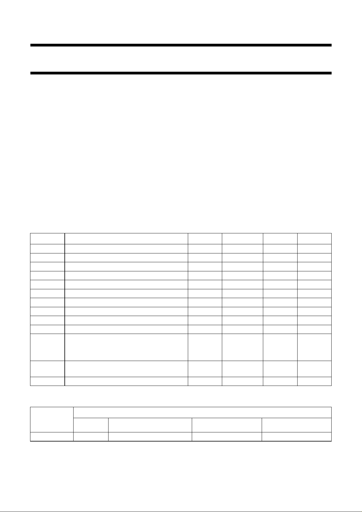
Fig.1 Block diagram.
April 1993 3
Page 4
Philips Semiconductors Product specification
NICAM-728 demodulator (NIDEM) TDA8732
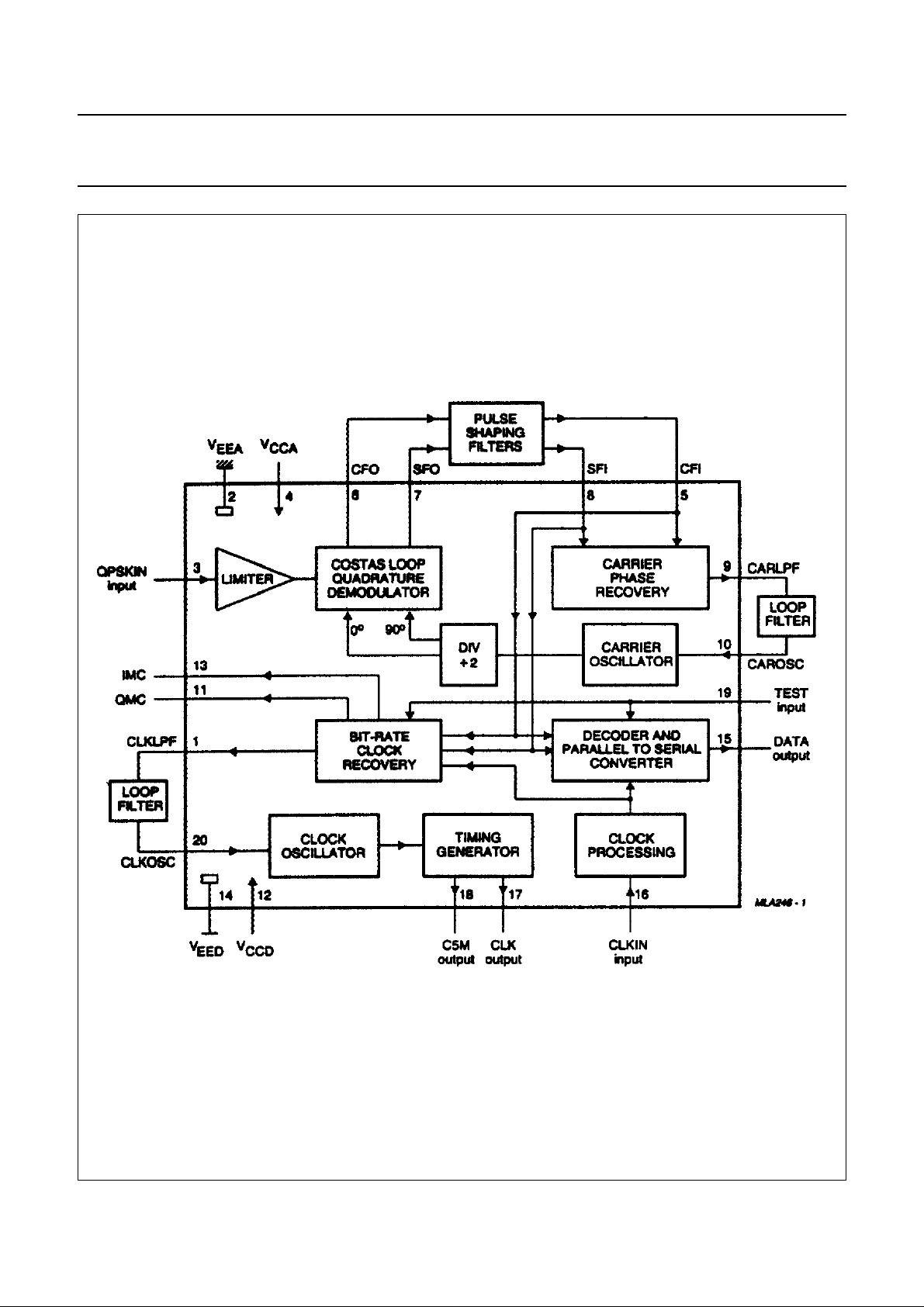
PINNING
SYMBOL PIN DESCRIPTION
CLKLPF 1 transconductance output for bit-rate loop low-pass filter
V
EEA
QPSKIN 3 QPSK modulated data input
V
CCA
CFI 5 baseband cosine channel input after filtering
CFO 6 demodulated cosine channel output to low-pass filter
SFO 7 demodulated sine channel output to low-pass filter
SFI 8 baseband sine channel input after filtering
CARLPF 9 transconductance output for carrier loop low-pass filter
CAROSC 10 crystal input for carrier oscillator (frequency is 11.7 MHz
QMC 11 monostable components connection for quadrature data
V
CCD
IMC 13 monostable components connection for in-phase data
V
EED
DATA 15 728 kbit/s demodulated and differentially decoded serial
CLKIN 16 bit-rate clock input at 728 kHz, phase-locked to the data
CLK 17 output clock frequency at 728 kHz
C5M 18 reference frequency output at
TEST 19 input for test purpose (grounded for normal operation)
CLKOS 20 crystal input for clock oscillator (frequency is 11.648 MHz)
2 ground for analog circuitry
4 power supply for analog circuitry
or 13.104 MHz)
transition detector
12 power supply for digital circuitry
transition detector
14 ground for digital circuitry
data output
5.824 MHz (8 x CLK)
Fig.2 Pin configuration.
April 1993 4
Page 5

Philips Semiconductors Product specification
NICAM-728 demodulator (NIDEM) TDA8732
FUNCTIONAL DESCRIPTION
QPSK demodulator
The DQPSK signal input to the demodulator (QPSKIN) is
limited and fed into the costas loop demodulator. A
single-pin carrier oscillator (CAROSC), at twice the carrier
frequency, supplies a differential signal to the divider
circuitry, which drives the demodulators with both 0° and
90° phase shift. This produces cosine and sine signals
which are required for the carrier recovery. Cosine
(in-phase) and sine (in Quadrature) channel baseband
filters are then provided externally between pins CFO and
CFI, and SFO and SFI respectively. The two filtered
baseband signals are then processed to provide an error
signal, the magnitude and which of which bear a fixed
relationship to the phase error of the carrier, regardless of
which of the four rest-states the signal occupies. The
carrier recovery loop is closed with the aid of a single pin
loop filter connection at CARLPF, which filters the error
voltage signal to control the 728 kHz as shown in
application diagrams Fig.4 and 5.
Bit-rate clock recovery loop
The CFI and SFI channels are processed using edge
detectors and monostables, with externally derived time
constants (see Fig.3), to generate a signal with a coherent
component at the data bit symbol rate. This signal is
compared with the clock derived from CLKIN and used to
produce an error signal at the transconductance output
CLKLPF. This error signal is loop-filtered and used to
control the clock generator (at CLKOSC if the on-board
clock is used; see Fig.5).
Clock oscillator and timing generator
A voltage-controlled oscillator on-board the NIDEM
operates at 11.648 MHz and is divided down to produce a
728 kHz (bit-rate) clock output (CLK) which is phase
locked to the pulse stream and may be used as an
alternative clock input for NIDEM. A reference clock at
5.824 MHz is provided at pin C5M (TTL levels).
Differential decoder and parallel-to-serial converter
The recovered symbol-rate clocking-signal (364 kHz)
produced internally is passed to the demodulator where it
samples the sliced raised cosine pulse stream. The
recovered bit-rate clocking-signal is passed to the decoder
and is used to differentially decode the demodulated data
signal and reform it into a serial bit-stream.
April 1993 5
Page 6

Philips Semiconductors Product specification
NICAM-728 demodulator (NIDEM) TDA8732
LIMITING VALUES
In accordance with the Absolute Maximum Rating System (IEC 134).
SYMBOL PARAMETER MIN. MAX. UNIT
V
CCA
V
CCD
QPSKIN modulated data input voltage −0.3 5.5 V
CFI baseband cosine channel input voltage −0.3 V
SFI baseband sine channel input voltage −0.3 V
CFO demodulated cosine channel output voltage −0.3 5.5 V
SFO demodulated sine channel output voltage −0.3 5.5 V
CAROSC crystal input voltage for carrier oscillator −0.3 5.5 V
CLKOSC crystal input voltage for clock oscillator −0.3 5.5 V
QMC,IMC monostable output voltage −0.3 V
DATA data output voltage −0.3 5.5 V
CLK clock output voltage −0.3 5.5 V
C5M reference frequency output voltage −0.3 5.5 V
CLKIN bit-rate clock input voltage −0.3 6 V
TEST input voltage for test purpose −0.3 6 V
CLKLPF bit-rate loop output voltage −0.3 5.5 V
CARLPF carrier loop output voltage −0.3 5.5 V
T
amb
T
stg
T
j
analog supply voltage −0.3 6 V
digital supply voltage −0.3 6 V
CCA
CCA
CCD
V
V
V
operating ambient temperature 0 70 °C
storage temperature −40 +125 °C
maximum junction temperature − +125 °C
THERMAL RESISTANCE
SYMBOL PARAMETER THERMAL RESISTANCE
R
th j-a
from junction to ambient in free air 80 K/W
April 1993 6
Page 7

Philips Semiconductors Product specification
NICAM-728 demodulator (NIDEM) TDA8732
CHARACTERISTICS
= 5 V ± 10%; V
V
CCA
SYMBOL PARAMETER CONDITIONS MIN. TYP. MAX. UNIT
Supply
V
CCA
V
CCD
V
CCA−VCCD
I
CCA
I
CCD
P
tot
analog supply voltage 4.5 5 5.5 V
digital supply voltage 4.5 5 5.5 V
differential supply voltage −0.5 − 0.5 V
analog supply current − 13 17 mA
digital supply current − 13 17 mA
total power dissipation − 130 187 mW
Inputs
CLKIN
V
IH
V
IL
I
IH
I
IL
QPSKIN
f
QPSKIN
R
I
C
I
SFI, CFI
I
b
R
I
C
I
CAROSC
f
car
CARRIER OSCILLATOR CRYSTAL
HIGH level input voltage 2 − V
LOW level input voltage −−0.8 V
HIGH level input current VI = 5 V −−10 µA
LOW level input current VI = 0 V −400 −−µA
input frequency 5 − 7 MHz
input resistance f = 6 MHz 1.75 2.5 3.25 kΩ
input capacitance f = 6 MHz − 2 − pF
input bias current V
input resistance f = 364 kHz 70 100 130 kΩ
input capacitance f = 364 kHz − 2 − pF
oscillator frequency 11.5 − 13.5 MHz
holder RW 43
nominal frequency with specified
load
f
PAL I
f
PAL B, G
PAL I − 13.104 − MHz
PAL B, G − 11.7 − MHz
vibration mode fundamental
circuit condition series resonance
adjustment tolerance on frequency
at 25 °C
temperature 0 − 70 °C
frequency stability over
temperature
C
L
load capacitance − 15 − pF
= 5 V ± 10%; −0.5 V < V
CCD
CCA
− V
SFI
V
CFI
C
= 15 pF
L
< 0.5 V; T
CCD
= 4.3 V;
= 4.3 V
= 0 to 70 °C; unless otherwise specified.
amb
CCD
−−5µA
−30 − +30 10
−30 − +30 10
V
−6
−6
April 1993 7
Page 8

Philips Semiconductors Product specification
NICAM-728 demodulator (NIDEM) TDA8732
SYMBOL PARAMETER CONDITIONS MIN. TYP. MAX. UNIT
R
s
C
m
C
p
CLKOSC
f
clk
BIT-RATE OSCILLATOR CRYSTAL
f
PAL I
f
PAL B, G
C
L
R
s
C
m
C
p
resonance resistance note 1 15 − 40 Ω
motional capacitance − 21 − fF
parallel capacitance −−5pF
drive power level −−0.5 mW
oscillator frequency Cl = 15 pF − 11.648 − MHz
holder RW 43
nominal frequency with specified
C
= 15 pF
L
load
PAL I − 11.648 − MHz
PAL B, G − 11.648 − MHz
vibration mode fundamental
circuit condition series resonance
adjustment tolerance on frequency
−30 − +30 10
−6
at 25 °C
temperature 0 − 70 °C
frequency stability over
−30 − +30 10
−6
temperature
load capacitance − 15 − pF
resonance resistance note 1 15 − 40 kΩ
motional capacitance − 21 − fF
parallel capacitance −−5pF
drive level −−0.5 mW
Outputs
CFO, SFO
R
O
V
amp
output impedance f = 364 kHz − 110 200 Ω
signal amplitude (peak-to-peak
value)
CARLPF
V
OL
V
OH
gm φ1 phase comparator
I
LO
LOW level output voltage IOL = 100 µA −−0.4 V
HIGH level output voltage IOH = −100 µAV
V
= 0.4 V to
O
transconductance gain
V
CCD
− 1 V
output leakage current for π/4
phase shift
CLKLPF
V
OL
LOW level output voltage IOL = 100 µA −−0.4 V
April 1993 8
0.8 1 − V
−1 V −−V
CCD
100 125 −µA/rd
−5 − 5 µA
Page 9

Philips Semiconductors Product specification
NICAM-728 demodulator (NIDEM) TDA8732
SYMBOL PARAMETER CONDITIONS MIN. TYP. MAX. UNIT
V
OH
gm φ2 phase comparator
I
LO
IMC, QMC (TYPICAL RC NETWORK; R =22KΩ;C=150PF)
t
REC
t
on
CLK, C5M
V
OL
V
OH
t
r
t
f
f
C5M
DATA
V
OL
V
OH
t
r
t
f
CLOCK TIMING
t
d
t
d
Note
1. Only the maximum value is relevant with a 15 Ω resistor in series with the crystal (due to the application
requirements).
HIGH level output voltage IOH = −100 µAV
V
= 0.4 V to
O
transconductance gain
V
CCD
−1 V
−1 V −−V
CCD
50 65 −µA/rd
off-state output leakage current −5 − 5 µA
monostable recovery time −−600 ns
monostable time − 1.37 −µs
LOW level output voltage IOL = 1 mA −−0.4 V
HIGH level output voltage IOH = −100 µA 2.4 − V
CCD
V
rise time CL = 15 pF; see Fig.3 − 20 − ns
fall time CL = 15 pF; see Fig.3 − 20 − ns
C5M reference frequency − 5.824 − MHz
LOW level output voltage IOL = 1 mA −−0.4 V
HIGH level output voltage IOH = −100 µA 2.4 − V
CCD
V
rise time CL = 15 pF; see Fig.3 − 30 − ns
fall time CL = 15 pF; see Fig.3 − 30 − ns
CLK to C5M delay (pin 17 to 18) − 15 − ns
CLKIN to DATA delay (pin 16 to 15) V
= 4.5 V − 520 585 ns
CCD
April 1993 9
Page 10

Philips Semiconductors Product specification
NICAM-728 demodulator (NIDEM) TDA8732
Fig.3 Data timing diagram.
April 1993 10
Page 11

Philips Semiconductors Product specification
NICAM-728 demodulator (NIDEM) TDA8732
April 1993 11
PAL B or G: 11.700 MHz
TH316BQM-3224QDBP (PAL I)
close as possible to the package.
(1) PAL I: 13.104 MHz
(2) 17.472 MHz
(3) TH316BQM-3223QDBP (PAL B or G)
(4) The 100 nF capacitor must be placed as
Fig.4 Typical application diagram with the SAA7280.
Page 12

Philips Semiconductors Product specification
NICAM-728 demodulator (NIDEM) TDA8732
April 1993 12
PAL B or G: 11.700 MHz
(1) PAL I: 13.104 MHz
TH316BQM-3224QDBP (PAL I)
close as possible to the package.
(2) 11.648 MHz
(3) TH316BQM-3223QDBP (PAL B or G)
(4) The 100 nF capacitor must be placed as
Fig.5 Typical application diagram with a NICAM decoder.
Page 13

Philips Semiconductors Product specification
NICAM-728 demodulator (NIDEM) TDA8732
PACKAGE OUTLINE
DIP20: plastic dual in-line package; 20 leads (300 mil)
D
seating plane
L
Z
20
pin 1 index
e
b
SOT146-1
M
E
A
2
A
A
1
w M
b
1
11
E
c
(e )
1
M
H
1
0 5 10 mm
scale
DIMENSIONS (inch dimensions are derived from the original mm dimensions)
A
A
A
UNIT
inches
Note
1. Plastic or metal protrusions of 0.25 mm maximum per side are not included.
max.
mm
OUTLINE
VERSION
SOT146-1
1 2
min.
max.
1.73
1.30
0.068
0.051
IEC JEDEC EIAJ
b
b
1
0.53
0.38
0.021
0.015
0.36
0.23
0.014
0.009
REFERENCES
cD E e M
(1) (1)
26.92
26.54
1.060
1.045
SC603
April 1993 13
6.40
6.22
0.25
0.24
10
(1)
M
e
L
1
3.60
8.25
3.05
7.80
0.14
0.32
0.12
0.31
EUROPEAN
PROJECTION
H
E
10.0
0.2542.54 7.62
8.3
0.39
0.010.10 0.30
0.33
ISSUE DATE
w
92-11-17
95-05-24
Z
max.
2.04.2 0.51 3.2
0.0780.17 0.020 0.13
Page 14

Philips Semiconductors Product specification
NICAM-728 demodulator (NIDEM) TDA8732
SOLDERING
Introduction
There is no soldering method that is ideal for all IC
packages. Wave soldering is often preferred when
through-hole and surface mounted components are mixed
on one printed-circuit board. However, wave soldering is
not always suitable for surface mounted ICs, or for
printed-circuits with high population densities. In these
situations reflow soldering is often used.
This text gives a very brief insight to a complex technology.
A more in-depth account of soldering ICs can be found in
“IC Package Databook”
our
Soldering by dipping or by wave
The maximum permissible temperature of the solder is
260 °C; solder at this temperature must not be in contact
DEFINITIONS
Data sheet status
Objective specification This data sheet contains target or goal specifications for product development.
Preliminary specification This data sheet contains preliminary data; supplementary data may be published later.
Product specification This data sheet contains final product specifications.
(order code 9398 652 90011).
with the joint for more than 5 seconds. The total contact
time of successive solder waves must not exceed
5 seconds.
The device may be mounted up to the seating plane, but
the temperature of the plastic body must not exceed the
specified maximum storage temperature (T
printed-circuit board has been pre-heated, forced cooling
may be necessary immediately after soldering to keep the
temperature within the permissible limit.
Repairing soldered joints
Apply a low voltage soldering iron (less than 24 V) to the
lead(s) of the package, below the seating plane or not
more than 2 mm above it. If the temperature of the
soldering iron bit is less than 300 °C it may remain in
contact for up to 10 seconds. If the bit temperature is
between 300 and 400 °C, contact may be up to 5 seconds.
stg max
). If the
Limiting values
Limiting values given are in accordance with the Absolute Maximum Rating System (IEC 134). Stress above one or
more of the limiting values may cause permanent damage to the device. These are stress ratings only and operation
of the device at these or at any other conditions above those given in the Characteristics sections of the specification
is not implied. Exposure to limiting values for extended periods may affect device reliability.
Application information
Where application information is given, it is advisory and does not form part of the specification.
LIFE SUPPORT APPLICATIONS
These products are not designed for use in life support appliances, devices, or systems where malfunction of these
products can reasonably be expected to result in personal injury. Philips customers using or selling these products for
use in such applications do so at their own risk and agree to fully indemnify Philips for any damages resulting from such
improper use or sale.
April 1993 14
 Loading...