

Page 1

INTEGRATED CIRCUITS
DATA SH EET
TDA8725T
Antenna signal processor
Product specification
File under Integrated Circuits, IC02
Philips Semiconductors
1995 Mar 21
Page 2

Philips Semiconductors Product specification
Antenna signal processor TDA8725T
FEATURES
• 75 Ω antenna input stage
• 75 Ω VCR RF input stage
• 75 Ω VCR tuner output
• 75 Ω TV tuner output.
For PIP applications, the antenna input signal is split and
fed to the main TV tuner and the PIP tuner. Good signal
suppression between the two outputs enables good quality
of the main picture when the PIP tuner is in use.
For VCR applications, the antenna input signal is split and
then fed directly to the VCR tuner and the TV tuner after
being combined with the VCR - RF signal. Good signal
GENERAL DESCRIPTION
The TDA8725T has been designed to split and combine
RF signals for Picture-In-Picture (PIP) and VCR
applications.
suppression between the two outputs enables good quality
pictures when the TV and VCR tuners are both operating.
Good signal suppression between the VCR input and the
antenna input reduces the amount of unwanted signal on
the antenna.
QUICK REFERENCE DATA
SYMBOL PARAMETER CONDITIONS MIN. TYP. MAX. UNIT
V
P
I
P
f
i
G
p
supply voltage (pins 8 and 9) 4.75 5.0 5.25 V
supply current (pins 8 and 9) − 65 − mA
input frequency 40 − 860 MHz
power gain
from antenna to VCR 3.5 5.0 6.5 dB
from antenna to TV 4 5.5 7 dB
from VCR − 0 − dB
F noise figure 6.5 9.0 10 dB
IP2 antenna linearity 2nd order
intercept point
IP3 antenna linearity 3rd order
intercept point
s
sup
signal suppression
at 40 MHz 137 140 − dBµV
at 860 MHz 119 124 − dBµV
at 40 MHz 121 124 − dBµV
at 860 MHz 108 111 − dBµV
VCR input to antenna 0 to 1 GHz 32 37 − dB
1 to 3 GHz 25 30 − dB
VCR output to TV output 0 to 300 MHz 35 40 − dB
300 to 860 MHz 22 27 − dB
TV output to VCR output 0 to 300 MHz 35 40 − dB
300 to 860 MHz 22 27 − dB
VSWR voltage standing wave ratio
at the antenna input − 2.5 4
at the outputs − 1.5 3
P
i(max)
maximum input power on antenna
−−10 − dBm
for 1 dB gain compression
1995 Mar 21 2
Page 3
Philips Semiconductors Product specification
Antenna signal processor TDA8725T
ORDERING INFORMATION
TYPE NUMBER
PACKAGE
NAME DESCRIPTION VERSION
TDA8725T SO16 plastic small outline package; 16 leads; body width 3.9 mm SOT109-1
BLOCK DIAGRAM
(1)
(2)
(1) TV tuner or main tuner.
(2) VCR tuner or PIP tuner.
Fig.1 Block diagram.
1995 Mar 21 3
Page 4

Philips Semiconductors Product specification
Antenna signal processor TDA8725T
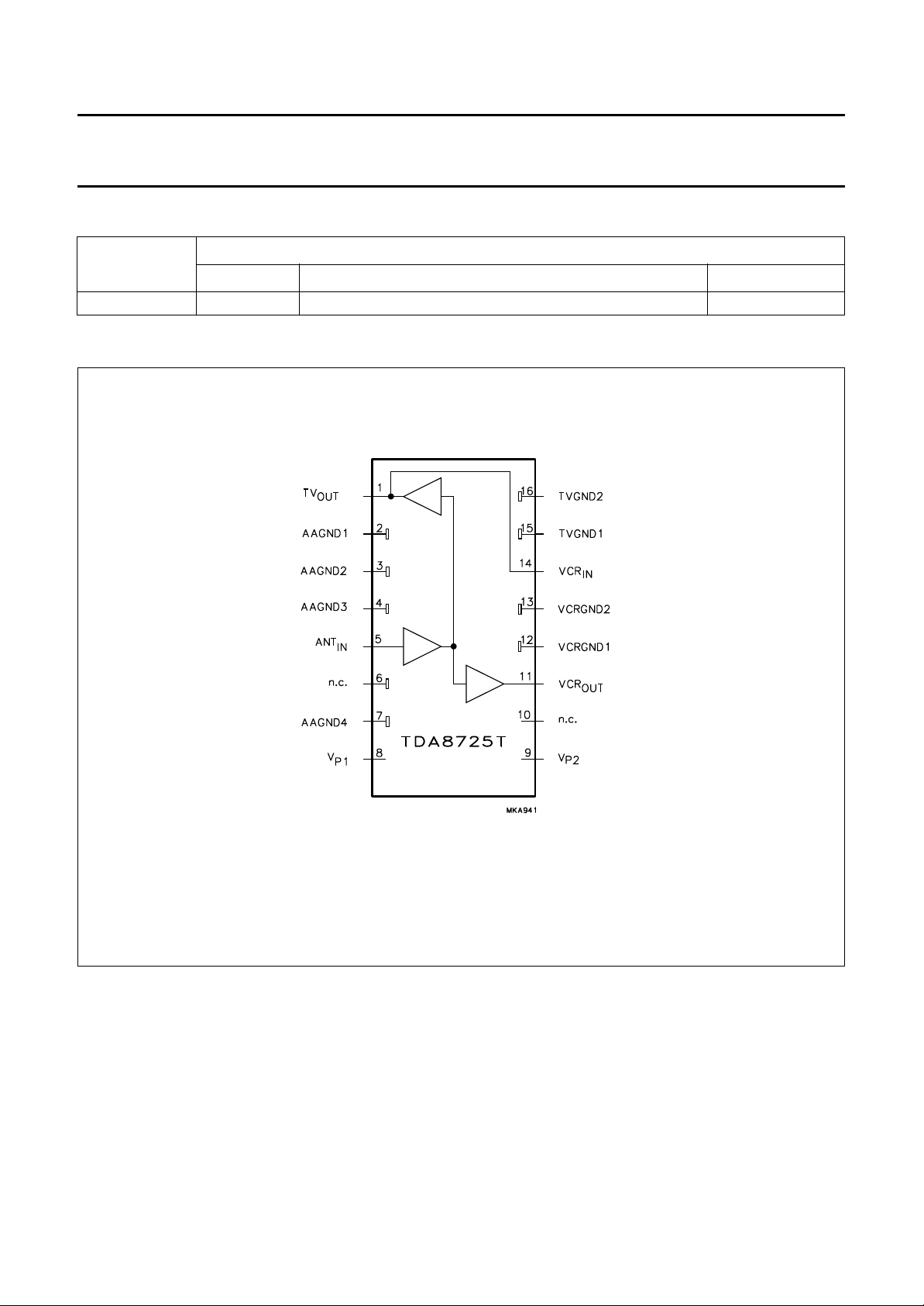
PINNING
SYMBOL PIN DESCRIPTION
TV
OUT
AAGND1 2 antenna amplifier ground 1
AAGND2 3 antenna amplifier ground 2
AAGND3 4 antenna amplifier ground 3
ANT
IN
n.c. 6 not connected
AAGND4 7 antenna amplifier ground 4
V
P1
V
P2
n.c. 10 not connected
VCR
OUT
VCRGND1 12 VCR amplifier ground 1
VCRGND2 13 VCR amplifier ground 2
VCR
IN
TVGND1 15 TV amplifier ground 1
TVGND2 16 TV amplifier ground 2
1 output to TV tuner (VCR+TV) and to
main tuner (PIP)
5 antenna input
8 power supply for the antenna
amplifier
9 power supply for the VCR output
amplifier
11 output to VCR and PIP tuner
14 VCR RF input
Fig.2 Pin configuration.
LIMITING VALUES
In accordance with the Absolute Maximum Rating System (IEC 134).
SYMBOL PARAMETER CONDITIONS MIN. MAX. UNIT
V
P
T
stg
T
amb
T
j
V
es
supply voltage −0.3 6 V
storage temperature −55 +150 °C
operating ambient temperature −10 +80 °C
junction temperature − +150 °C
electrostatic handling note 1 −2000 +2000 V
note 2 −200 +200 V
Notes
1. Human Body Model: UZW-BO/FQ-A302 (R = 1500 Ω, C = 100 pF). The IC withstands the ESD test class 2 (2000 V).
2. Machine Model: UZW-BO/FQ-B302 (R = 0 Ω, C = 200 pF). All pins withstand 200 V.
THERMAL CHARACTERISTICS
SYMBOL PARAMETER VALUE UNIT
R
th j-a
thermal resistance from junction to ambient in free air 115 K/W
1995 Mar 21 4
Page 5

Philips Semiconductors Product specification
Antenna signal processor TDA8725T
CHARACTERISTICS
V
=5V; T
P
SYMBOL PARAMETER CONDITIONS MIN. TYP. MAX. UNIT
V
P
I
P
f
i
G
p
F noise figure 6.5 9.0 10 dB
IP2 antenna linearity 2nd order
IP3 antenna linearity 3rd order
s
sup
VSWR voltage standing wave ratio
P
i(max)
=25°C; measured in circuit of Fig.4; unless otherwise specified.
amb
supply voltage (pins 8 and 9) 4.75 5.0 5.25 V
supply current (pins 8 and 9) 55 65 75 mA
input frequency 40 − 860 MHz
power gain 40 to 860 MHz
from antenna to VCR 3.5 5.0 6.5 dB
from antenna to TV 4 5.5 7 dB
from VCR − 0 − dB
at 40 MHz 137 140 − dBµV
intercept point
at 860 MHz 119 124 − dBµV
at 40 MHz 121 124 − dBµV
intercept point
at 860 MHz 108 111 − dBµV
signal suppression
VCR input to antenna 0 to 1 GHz 32 37 − dB
1 to 3 GHz 25 30 − dB
VCR output to TV output 0 to 300 MHz 35 40 − dB
300 to 860 MHz 22 27 − dB
TV output to VCR output 0 to 300 MHz 35 40 − dB
300 to 860 MHz 22 27 − dB
at the antenna input − 2.5 4
at the outputs − 1.5 3
maximum input power on antenna
−−10 − dBm
for 1 dB gain compression
1995 Mar 21 5
Page 6

Philips Semiconductors Product specification
Antenna signal processor TDA8725T
Fig.3 Reflection coefficient (S11) antenna input.
1995 Mar 21 6
Page 7

Philips Semiconductors Product specification
Antenna signal processor TDA8725T
APPLICATION INFORMATION
Fig.4 Picture-in-picture (PIP) application.
1995 Mar 21 7
Page 8

Philips Semiconductors Product specification
Antenna signal processor TDA8725T
Fig.5 VCR and TV application.
1995 Mar 21 8
Page 9

Philips Semiconductors Product specification
Antenna signal processor TDA8725T
PACKAGE OUTLINE
SO16: plastic small outline package; 16 leads; body width 3.9 mm
D
c
y
Z
16
pin 1 index
1
e
9
8
w M
b
p
SOT109-1
E
H
E
A
2
A
1
L
detail X
A
X
v M
A
Q
(A )
L
p
A
3
θ
0 2.5 5 mm
scale
DIMENSIONS (inch dimensions are derived from the original mm dimensions)
mm
OUTLINE
VERSION
SOT109-1
A
max.
1.75
0.069
A1A2A
0.25
1.45
0.10
1.25
0.0098
0.057
0.0039
0.049
IEC JEDEC EIAJ
076E07S MS-012AC
0.25
0.01
b
3
p
0.49
0.25
0.36
0.19
0.0098
0.019
0.0075
0.014
UNIT
inches
Note
1. Plastic or metal protrusions of 0.15 mm maximum per side are not included.
(1)E(1) (1)
cD
10.0
4.0
3.8
0.16
0.15
1.27
0.050
9.8
0.39
0.38
REFERENCES
1995 Mar 21 9
eHELLpQZywv θ
1.05
0.041
1.0
0.4
0.039
0.016
0.7
0.25
0.6
0.028
0.01 0.004
0.020
EUROPEAN
PROJECTION
0.25 0.1
0.01
0.7
0.3
0.028
0.012
ISSUE DATE
91-08-13
95-01-23
o
8
o
0
6.2
5.8
0.24
0.23
Page 10

Philips Semiconductors Product specification
Antenna signal processor TDA8725T
SOLDERING
Plastic small-outline packages
YWAVE
B
During placement and before soldering, the component
must be fixed with a droplet of adhesive. After curing the
adhesive, the component can be soldered. The adhesive
can be applied by screen printing, pin transfer or syringe
dispensing.
Maximum permissible solder temperature is 260 °C, and
maximum duration of package immersion in solder bath is
10 s, if allowed to cool to less than 150 °C within 6 s.
Typical dwell time is 4 s at 250 °C.
A modified wave soldering technique is recommended
using two solder waves (dual-wave), in which a turbulent
wave with high upward pressure is followed by a smooth
laminar wave. Using a mildly-activated flux eliminates the
need for removal of corrosive residues in most
applications.
Y SOLDER PASTE REFLOW
B
Reflow soldering requires the solder paste (a suspension
of fine solder particles, flux and binding agent) to be
applied to the substrate by screen printing, stencilling or
pressure-syringe dispensing before device placement.
Several techniques exist for reflowing; for example,
thermal conduction by heated belt, infrared, and
vapour-phase reflow. Dwell times vary between 50 and
300 s according to method. Typical reflow temperatures
range from 215 to 250 °C.
Preheating is necessary to dry the paste and evaporate
the binding agent. Preheating duration: 45 min at 45 °C.
R
EPAIRING SOLDERED JOINTS (BY HAND-HELD SOLDERING
IRON OR PULSE
-HEATED SOLDER TOOL)
Fix the component by first soldering two, diagonally
opposite, end pins. Apply the heating tool to the flat part of
the pin only. Contact time must be limited to 10 s at up to
300 °C. When using proper tools, all other pins can be
soldered in one operation within 2 to 5 s at between 270
and 320 °C. (Pulse-heated soldering is not recommended
for SO packages.)
For pulse-heated solder tool (resistance) soldering of VSO
packages, solder is applied to the substrate by dipping or
by an extra thick tin/lead plating before package
placement.
DEFINITIONS
Data sheet status
Objective specification This data sheet contains target or goal specifications for product development.
Preliminary specification This data sheet contains preliminary data; supplementary data may be published later.
Product specification This data sheet contains final product specifications.
Limiting values
Limiting values given are in accordance with the Absolute Maximum Rating System (IEC 134). Stress above one or
more of the limiting values may cause permanent damage to the device. These are stress ratings only and operation
of the device at these or at any other conditions above those given in the Characteristics sections of the specification
is not implied. Exposure to limiting values for extended periods may affect device reliability.
Application information
Where application information is given, it is advisory and does not form part of the specification.
LIFE SUPPORT APPLICATIONS
These products are not designed for use in life support appliances, devices, or systems where malfunction of these
products can reasonably be expected to result in personal injury. Philips customers using or selling these products for
use in such applications do so at their own risk and agree to fully indemnify Philips for any damages resulting from such
improper use or sale.
1995 Mar 21 10
 Loading...