

Page 1

INTEGRATED CIRCUITS
DATA SH EET
TDA8722
2
I
C-bus programmable modulator
for negative video modulation and
FM sound
Objective specification
File under Integrated Circuits, IC02
Philips Semiconductors
1995 Mar 21
Page 2
Philips Semiconductors Objective specification
I2C-bus programmable modulator for
negative video modulation and FM sound
FEATURES
• Video amplifier with clamp and white clip circuits
• FM sound modulator
• Asymmetrical and symmetrical RF outputs available
• Symmetrical RF oscillator using only a few external
components
• External adjusting of modulation depth and level of the
sound subcarrier
• I2C-bus receiver for frequency setting and test-mode
selection
2
• One I
• On-chip Phase-Locked Loop (PLL) frequency
• On-chip power supply regulator
• Bus switchable oscillator
• On-chip Test Pattern Signal Generator (TPSG).
C programmable output port
synthesizer
GENERAL DESCRIPTION
The TDA8722 is a programmable modulator which
generates an RF TV channel from a baseband video
signal and a baseband audio signal in the event of
negative video and FM sound standards (PAL B/G, I, D/K
and NTSC).
It is especially suited for satellite receivers, video
recorders and cable converters. The video carrier
frequency is set exactly to the correct channel frequency
by a PLL synthesizer which is programmed in accordance
with the I
2
C-bus format.
TDA8722
APPLICATIONS
• Video recorders
• Cable converters
• Satellite receivers.
ORDERING INFORMATION
TYPE
NUMBER
TDA8722T SO20 plastic small outline package; 20 leads; body width 7.5 mm SOT163-1
TDA8722M SSOP20 plastic shrink small outline package; 20 leads; body width 4.4 mm SOT266-1
NAME DESCRIPTION VERSION
PACKAGE
1995 Mar 21 2
Page 3

Philips Semiconductors Objective specification
I2C-bus programmable modulator for
TDA8722
negative video modulation and FM sound
QUICK REFERENCE DATA
V
DDA=VDDD
SYMBOL PARAMETER CONDITIONS MIN. TYP. MAX. UNIT
V
DDA
V
DDD
I
DD
∆m typical modulation depth range video level (pin 19) = 0.5 V (p-p);
∆P/S typical picture-to-sound level
V
RF
δf FM deviation on audio
Notes
1. Value depends on value of resistor R17 (see Fig.7).
2. Value depends on value of capacitor C17 (see Fig.7).
=5V; T
=25°C after the IC has reached thermal equilibrium; unless otherwise specified.
amb
analog supply voltage 4.5 5.0 5.5 V
digital supply voltage 4.5 5.0 5.5 V
total supply current normal mode 41 52 63 mA
65 − 90 %
note 1; see Fig.10
note 2; see Fig.11 −18 −−10 dB
range
RF output voltage level
asymmetrical on a 75 Ω load
subcarrier
frequency between
471.25 and 855.25 MHz
= 400 Hz; V1= 0.5 V (RMS);
f
i
before pre-emphasis filter
77 80 83 dBµV
20 25 30 kHz
1995 Mar 21 3
Page 4
Philips Semiconductors Objective specification
I2C-bus programmable modulator for
negative video modulation and FM sound
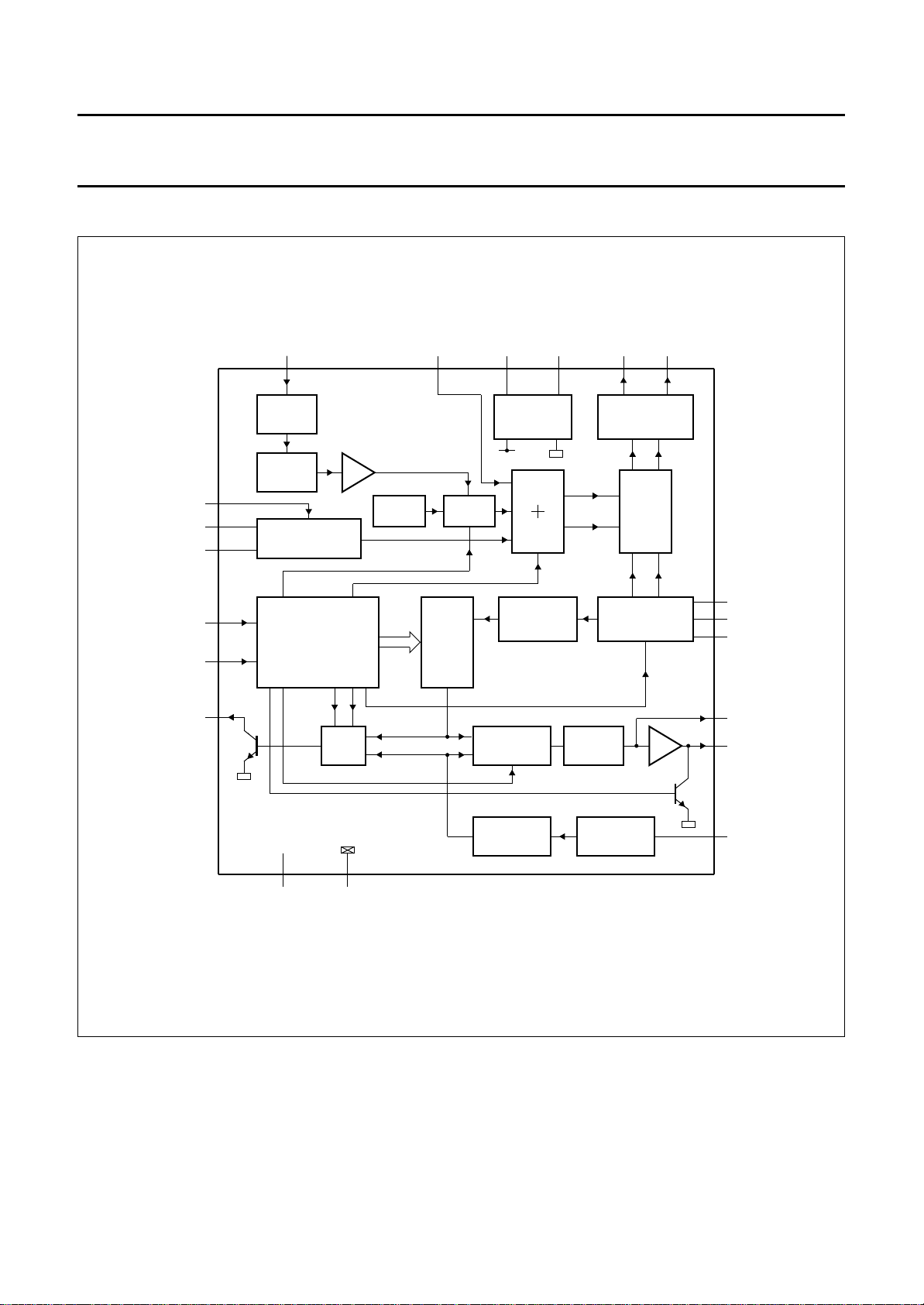
BLOCK DIAGRAM
handbook, full pagewidth
AUDIO
SOSCA
SOSCB
SDA
SCL
1
2
3
13
12
VIDEO
19
CLAMP
VIDEO AMP
CLIP
AUDIO
FM MODULATOR
2
I C-BUS
RECEIVER
TDA8722
ADJUST AGNDVDDA
TPSG
10 bits
TPSG on
12-BIT
DIVIDER
(N)
SWITCH
18 2017
VOLTAGE
REGULATOR
balance test
PRESCALER
(8)
RFA RFB
16 15
ASYMMETRICAL
OUTPUT
BUFFER
MIXER
PC
UHF
OSCILLATOR
TDA8722
6
UOSCA
5
OGND
4
UOSCB
P0
14
enable/
select
LOGIC
11
V
DDD DGND
f
DIV
f
ref
31.25 kHz
10
RF oscillator on
PHASE
DETECTOR
enable
DIVIDER
(M = 128)
CHARGE
PUMP
4 MHz
OSCILLATOR
AMP
MBE401
8
CP
7
AMP
9
XTAL
Fig.1 Block diagram.
1995 Mar 21 4
Page 5
Philips Semiconductors Objective specification
I2C-bus programmable modulator for
negative video modulation and FM sound
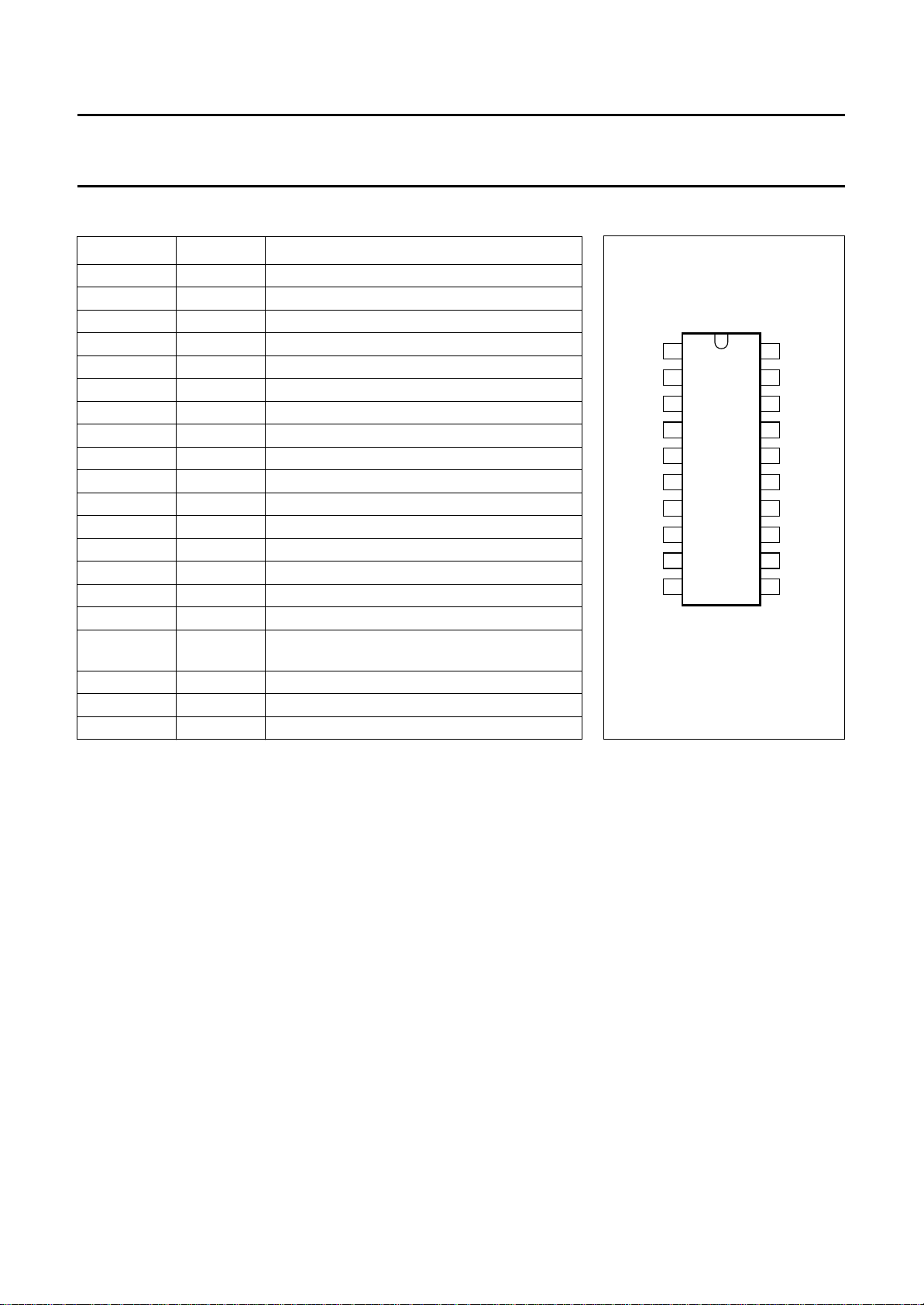
PINNING
SYMBOL PIN DESCRIPTION
AUDIO 1 audio input
SOSCA 2 sound oscillator A
SOSCB 3 sound oscillator B
UOSCB 4 UHF oscillator B
OGND 5 RF oscillator ground
UOSCA 6 UHF oscillator A
AMP 7 tuning amplifier output
CP 8 charge pump output
XTAL 9 crystal oscillator
DGND 10 digital ground
V
DDD
SCL 12 serial clock input (I
SDA 13 serial data input (I
P0 14 NPN open-collector output Port
RFB 15 asymmetrical RF output B
RFA 16 asymmetrical RF output A
ADJUST 17 modulation depth and picture-to-sound
AGND 18 analog ground
VIDEO 19 video input
V
DDA
11 digital supply voltage
2
C-bus)
2
C-bus)
distance adjustment pin
20 analog supply voltage
TDA8722
page
AUDIO
SOSCA VIDEO
SOSCB AGND
UOSCB ADJUST
UOSCA RFB
1
2
3
4
5
OGND RFA
AMP P0
CP
XTAL SCL
DGND
6
7
8
9
10
TDA8722
20
19
18
17
16
15
14
13
12
11
MBE394
Fig.2 Pin configuration.
V
DDA
SDA
V
DDD
FUNCTIONAL DESCRIPTION
The TDA8722 is a programmable modulator which can be
divided into two main blocks:
• A modulator for negative video modulation and
FM sound TV standards
• A programmable PLL frequency synthesizer.
The video part of the modulator consists of a clamping
circuit which sets the internal reference voltage to the
bottom of the synchronizing pulse, followed by a white clip
which avoids over modulation in case the video signal is
too strong. Typically, the IC starts to clip the video signal
when the voltage at the video input (pin 19) is
>560 mV (p-p) while the normal voltage at the video input
is 500 mV (p-p). This clipping function ensures that the
video modulation depth is not too high. The modulation
depth is adjusted in the application between at least
65 and 90% by changing the resistor value between pin 17
and ground (R17). The value can change between 47 kΩ
and infinite (R17 removed); see Fig.10.
1995 Mar 21 5
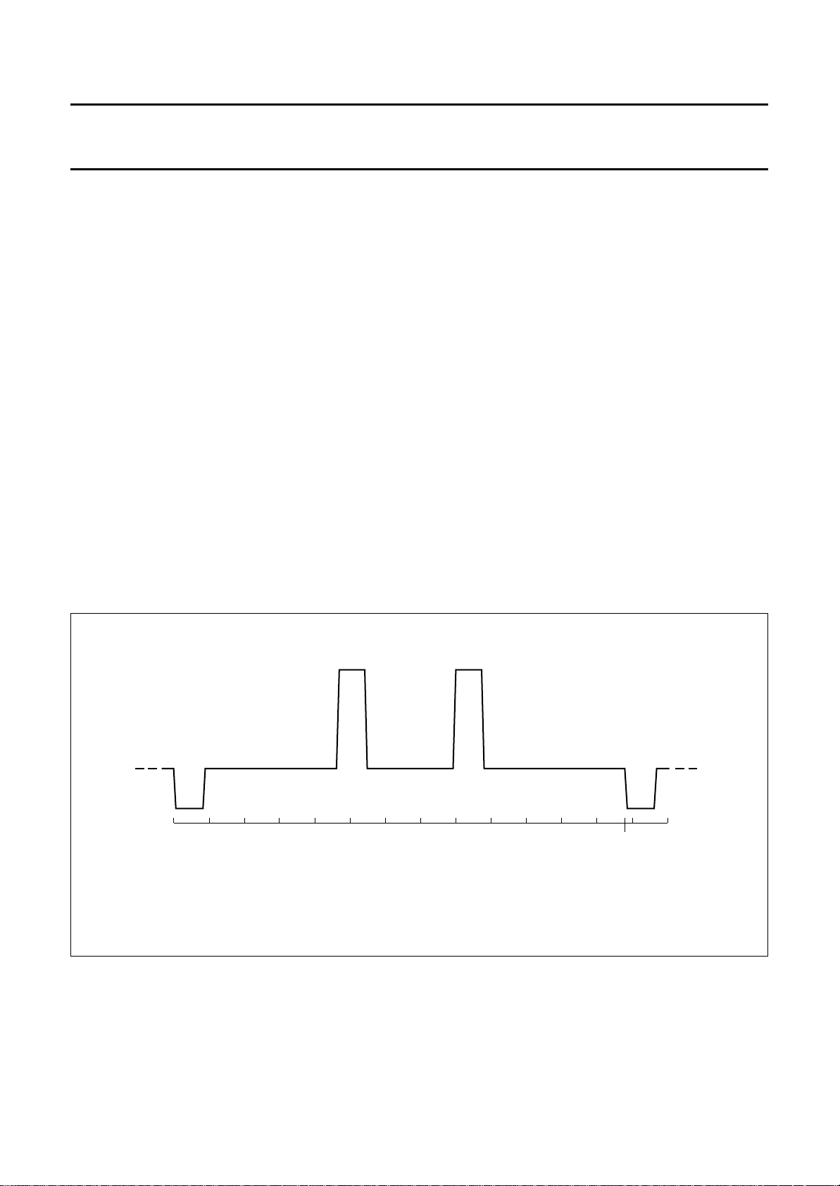
The video part also contains a test pattern signal generator
to simplify the adjustment of the receiving channel of the
TV set to the required channel of the modulator. The
pattern consists of a synchronization pulse and two
vertical white bars on screen (see Fig.3).
The audio part of the modulator contains an FM sound
modulator. The frequency of the sound subcarrier is set in
the application by external components (C3, L3 and R3).
The difference between the video carrier level and the
sound subcarrier level is adjusted in the application by
changing the value of the capacitor between pin 17 and
ground (C17). The value can change between
0 and 47 pF. The distance between the video carrier and
the sound subcarrier can be adjusted between at least
−10 and −18 dB (see Fig.11).
To bias the audio input it is necessary to put a resistor in
the application between pin 1 and ground. The resistor has
a typical value of 12 kΩ.
Page 6
Philips Semiconductors Objective specification
I2C-bus programmable modulator for
negative video modulation and FM sound
The RF part of the oscillator consists of:
• An oscillator which operates at the required video carrier
frequency. The range of the oscillator is determined in
the application by C5, C6, L5 and D5.
• An RF mixer. It first combines the video signal and the
sound subcarrier to build a baseband TV channel. Then
the baseband signal is mixed with the oscillator signal to
get the RF TV channel. The mixer has two outputs
which can be used as two independent asymmetrical
outputs, or as one symmetrical output. In the event of
asymmetrical use, the unused output must be loaded
with a 75 Ω resistor (see Fig.7).
The oscillator frequency is set by a programmable PLL
frequency synthesizer in accordance with equation:
f
=8×N×f
osc
Where:
f
is the local oscillator frequency.
osc
N is a 12-bit dividing number (10 bits are programmable
by the I2C-bus).
f
is the crystal frequency (4 MHz) divided by 128
ref
(31.25 kHz).
ref
TDA8722
The circuit allows a step of 250 kHz but because only
10 bits are programmable, the programming steps are
1 MHz.
When the PLL loop is locked, both inputs of the phase
comparator are equal, which gives equation:
f
f
DIV
osc
===
------------8N×
During the test mode operation, f
monitored on the output Port pin (pin 14).
Software information
The synthesizer is controlled via a two-wire I
receiver. For programming, the address byte (C8 HEX)
has to be sent first. Then one or two data bytes are used
to set the 10 programmable bits of the dividing number N,
the test bits (see Table 1) and the output Port state. Note
that after power-up of the IC, the two data bytes must be
sent.
f
xtal
--------- 128
f
ref
DIV
and f
can be
ref
2
C-bus
handbook, full pagewidth
010203040 50 60
t (µs)
Fig.3 Test pattern signal.
MBE395
64
70
1995 Mar 21 6
Page 7
Philips Semiconductors Objective specification
I2C-bus programmable modulator for
TDA8722
negative video modulation and FM sound
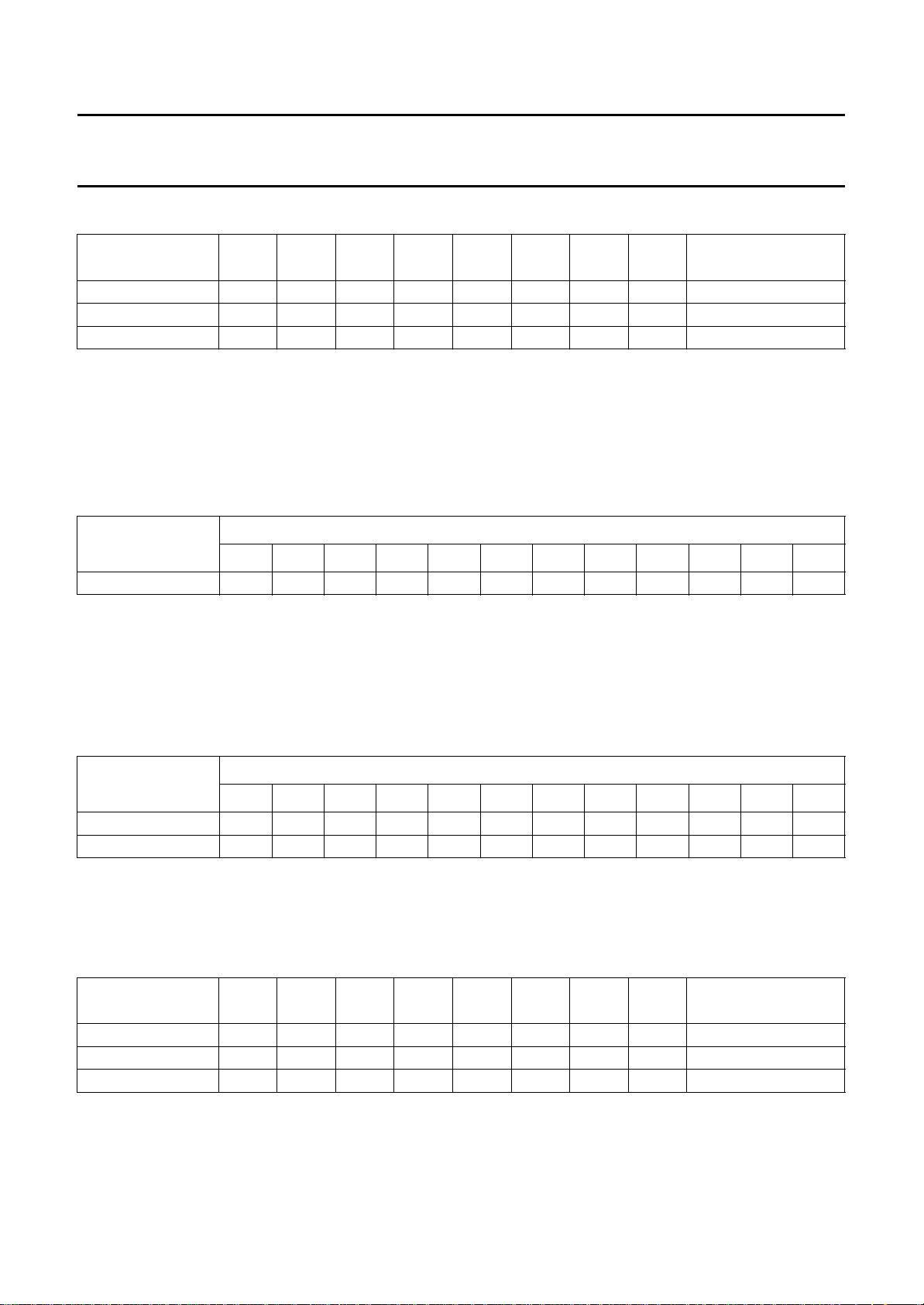
Table 1 Data format; notes 1 and 2
BYTE
BIT 7
MSB
BIT 6 BIT 5 BIT 4 BIT 3 BIT 2 BIT 1
Address byte C8 1 1001000 ACK
Data byte 1 0 b11 b10 b9 b8 b7 b6 b5 ACK
Data byte 2 1 T0
(3)
T1
(3)
T2
(3)
P0
(4)
b4 b3 b2 ACK
Notes
1. The 10 programmable bits of N are: b2 to b11.
2. Internal hardware sets: b1 = 0 and b0 = 1.
3. T0, T1 and T2 are bits used for test purposes (see Table 5).
4. P0 is a bit used for controlling the state of the output Port (see Table 6).
Table 2 Structure of the dividing number N
(1)
BITS
RESULT
b11 b10 b9 b8 b7 b6 b5 b4 b3 b2 b1
Frequency (MHz)
(3)
512 256 128 64 32 16 8 4 2 1 0.5 0.25
BIT 0
LSB
ACKNOWLEDGE BIT
(2)
b0
(2)
Notes
1. Bits b2 to b11 are programmable and represent the integer part of the frequency in MHz. Bits b1 and b0 are fixed
internally to b1 = 0 and b0 = 1 to get the added 0.25 MHz, common for most TV channels.
2. Bits b1 and b0 are not programmable.
3. f
= 512b11 + 256b10 + 128b9 + 64b8 + 32b7 + 16b6 + 8b5 + 4b4 + 2b3 + b2 + 0.25 (MHz).
osc
Table 3 Dividing number N for programming channel 21 (471.25 MHz)
BITS
RESULT
b11 b10 b9 b8 b7 b6 b5 b4 b3 b2 b1
(1)
b0
(1)
Value 011101011101
(2)
Frequency (MHz)
025612864016042100.25
Notes
1. Bits b1 and b0 are not programmable.
2. f
=0+256+128+64+0+16+0+4+2+1+0.25 (MHz) = 471.25 MHz.
osc
Table 4 Content of the data bytes to program channel 21 (471.25 MHz)
BYTE
BIT 7
MSB
BIT 6 BIT 5 BIT 4 BIT 3 BIT 2 BIT 1
BIT 0
LSB
ACKNOWLEDGE BIT
Address byte C8 1 1 0 0 1 0 0 0 ACK
Data byte 1 0 0 1 1 1 0 1 0 ACK
Data byte 2 1 0 0 0 0 1 1 1 ACK
1995 Mar 21 7
Page 8
Philips Semiconductors Objective specification
I2C-bus programmable modulator for
TDA8722
negative video modulation and FM sound
It is possible to change only one data byte. The circuit will recognize which one is received with the value of MSB
(0 for data byte 1 and 1 for data byte 2). It is possible to change the frequency by 1 MHz with data byte 2. It is easy to
increment the channel frequency when its frequency width is 8 MHz by simply incrementing data byte 1.
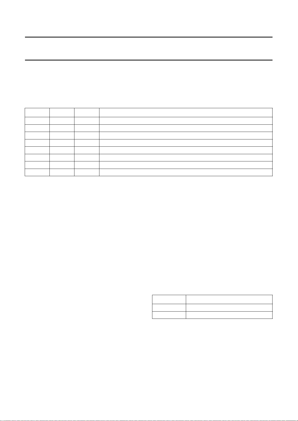
The bits T0 to T2 are available for test purposes and the possibilities are shown in Table 5.
Table 5 Test modes
T0 T1 T2 OPERATIONAL MODE
0 0 0 normal operation
0 0 1 Test Pattern Signal Generator (TPSG) on; note 1
0 1 0 RF oscillator off; note 2
0 1 1 balance test; note 3
100f
1 0 1 high-impedance test; note 5
110f
1 1 1 phase detector disabled; baseband signals on RF outputs; note 6
Notes
1. In ‘TPSG on’ mode the video carrier is modulated by the test signal consisting of a synchronization pulse and two
vertical white bars on a black screen. This mode should be selected to adjust the TV set receiving the modulated
signal to the right frequency.
2. In ‘RF oscillator off’ mode, the RF oscillator and the RF mixer are switched-off and there is no RF carrier coming out
of the device. This mode can be selected to avoid RF radiation to other parts when the modulator output is not used.
3. In ‘balance test’, the video carrier is over modulated. This simplifies residual carrier measurements.
4. In ‘f
f
DIV
’ and ‘f
ref
is available on the output Port pin. This mode requires that bit P0 = 0.
’ modes, the reference frequency f
DIV
5. The ‘high-impedance test’ mode may be used to inject an external tuning voltage to the RF tank circuit, to test the
oscillator. In this mode, the phase detector is disabled and the external transistor of the tuning amplifier is
switched-off. The AMP output (pin 7) is LOW (<200 mV).
6. In the ‘phase detector disabled’ mode, it is possible to measure the leakage current at the input of the tuning amplifier,
on the CP pin. In this mode the RF oscillator is off, and the baseband TV channel signal is present on the RF outputs
for testing the audio and video parts.
out (if p0 = 0); note 4
ref
out (if p0 = 0); note 4
DIV
ref
in the phase comparator or the divided RF oscillator frequency
The possibilities of bit P0, which controls the output Port
(pin 14) are given in Table 6.
The Port is an NPN open-collector type. For monitoring the
f
or f
ref
frequency on the output Port, the P0 bit must be
DIV
logic 0 to let the output Port free.
1995 Mar 21 8
Table 6 Output Port programming
P0 OUTPUT PORT STATE
0 off; high impedance
1 on; sinking current
Page 9

Philips Semiconductors Objective specification
I2C-bus programmable modulator for
TDA8722
negative video modulation and FM sound
LIMITING VALUES
In accordance with the Absolute Maximum Rating System (IEC 134).
SYMBOL PARAMETER MIN. MAX. UNIT
V
DDA
V
DDD
V
DD
V
max
T
stg
T
amb
HANDLING
Inputs and outputs are protected against electrostatic discharge in normal handling. However, to be completely safe, it
is desirable to take normal precautions appropriate to handling integrated circuits. Every pin withstands the ESD test in
accordance with
Semiconductors Machine Model (MM) 0 Ω, 200 pF (200 V).
THERMAL RESISTANCE
analog supply voltage −0.3 +6 V
digital supply voltage −0.3 +6 V
operating supply voltage 4.5 5.5 V
maximum voltage on all pins −0.3 V
DD
IC storage temperature −40 +125 °C
operating ambient temperature −20 +85 °C
“MIL-STD-883C category B”
(2000 V). Every pin withstands the ESD test in accordance with Philips
V
SYMBOL PARAMETER VALUE UNIT
R
th j-a
thermal resistance from junction to ambient in free air
SO20; SOT163-1 85 K/W
SSOP20; SOT266-1 120 K/W
1995 Mar 21 9
Page 10
Philips Semiconductors Objective specification
I2C-bus programmable modulator for
TDA8722
negative video modulation and FM sound
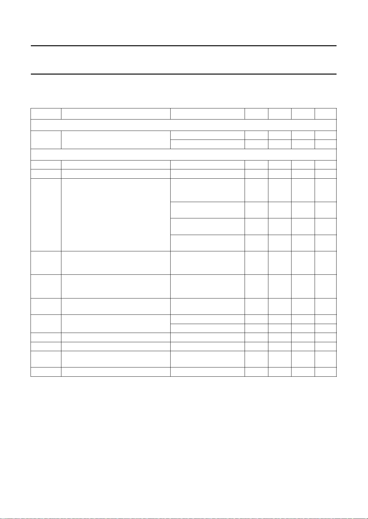
CHARACTERISTICS
V
DDA=VDDD
unless otherwise specified.
SYMBOL PARAMETER CONDITIONS MIN. TYP. MAX. UNIT
Supply
I
DD
Video characteristics
I
19
z
19
m modulation depth V
∆m modulation depth range V
∆m
APL
V
clip(p-p)
S/N video video signal-to-noise ratio f
G
diff
φ
diff
V/S video-to-sync ratio V
f
video
=5V; T
=25°C; valid over the whole UHF band; measured in circuit of Fig.7;
amb
supply current normal mode 41 52 63 mA
RF off test mode 30 38 46 mA
input current (AC) V19= 3.2 V − 0.5 2.0 µA
video input impedance V19= 3.2 V 30 −−kΩ
= 500 mV (p-p) EBU
19
77 82 87 %
colour bars; R17 = 120 kΩ;
see Fig.7
during clipping condition;
85 − 98 %
note 1
TPSG mode;
72 82 92 %
R17 = 120 kΩ
balance test mode;
110 −−%
R17 = 120 kΩ
= 500 mV (p-p) EBU
19
65 − 90 %
colour bars;
47 kΩ≤R17 ≤∞
variation of modulation depth with
change of APL between 10 and 90%
referenced to the value for
APL = 50%;
−2 − +2 %
V19= 500 mV (p-p)
video input level where clipping starts
(peak-to-peak value)
video level on pin 19;
− 0.56 − V
note 2
< 700 MHz; note 3 48 52 − dB
RF
> 700 MHz; note 3 46 50 − dB
f
RF
differential gain note 4 −8 − +8 %
differential phase note 4 −8 − +8 deg
= 500 mV (p-p);
19
6.9/3.1 7/3 7.1/2.9
V/S = 7/3
frequency response for the video signal note 5 −1 − +1 dB
1995 Mar 21 10
Page 11
Philips Semiconductors Objective specification
I2C-bus programmable modulator for
TDA8722
negative video modulation and FM sound
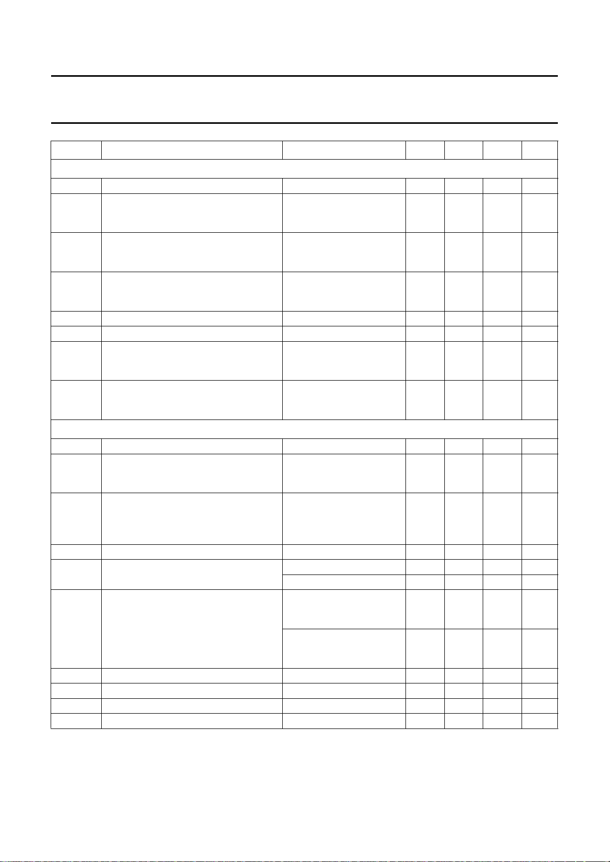
SYMBOL PARAMETER CONDITIONS MIN. TYP. MAX. UNIT
Audio characteristics (for PAL G standard; audio subcarrier at 5.5 MHz)
Z
1
δm modulation deviation f
δm
max
THD total harmonic distortion f
S/N audio audio signal-to-noise ratio note 6 45 50 − dB
f
audio
P/S picture-to-sound ratio no audio signal;
∆P/S picture-to-sound ratio range no audio signal;
audio input impedance 30 −−kΩ
= 400 Hz;
1
20 25 30 kHz
V1= 0.5 V (RMS) before
pre-emphasis filter
maximum modulation deviation f1= 400 Hz;
60 85 − kHz
V1= 2.0 V (RMS) before
pre-emphasis filter
= 1 kHz;
1
− 0.4 1.5 %
V1= 0.5 V (RMS) before
pre-emphasis filter
frequency response of the audio signal note 7 −1 − +1 dB
−16 −13 −10 dB
FM = 5.5 MHz;
C17=15pF
−18 −−10 dB
FM = 5.5 MHz;
0pF≤C17 ≤ 39 pF
Channel characteristics
f
RF
V
RF
RF frequency range using tank circuit of Fig.7 471.25 − 855.25 MHz
output level on RFA and RFB asymmetrical output
77 80 83 dBµV
loaded with 75 Ω;
f = 471.25 to 855.25 MHz
∆V
RF
difference between the level of
modulated carrier and the level of the
unmodulated carrier
measurement is made
during synchronization
pulse for the modulated
012dB
carrier
SPO spurious outside channel note 8 −−62 − dBc
RF
SC
sh
RF second harmonic level on
asymmetrical output
sh
sound carrier second harmonic level fs= 5.5 MHz;
fRF= 471.25 MHz −−30 −25 dBc
= 855.25 MHz −−20 −15 dBc
f
RF
−−65 −60 dBc
C17 = 15 pF;
fRF< 700 MHz
= 5.5 MHz;
f
s
−−63 −58 dBc
C17 = 15 pF;
fRF> 700 MHz
SC
th
sound carrier third harmonic level fs= 5.5 MHz; C17 = 15 pF −−65 −60 dBc
video signal harmonics note 9 −−60 −55 dBc
f
ref
reference frequency spurious fp+ 31.25 kHz −−65 −60 dBc
IM chrominance beat note 10 −−65 −60 dBc
1995 Mar 21 11
Page 12
Philips Semiconductors Objective specification
I2C-bus programmable modulator for
TDA8722
negative video modulation and FM sound
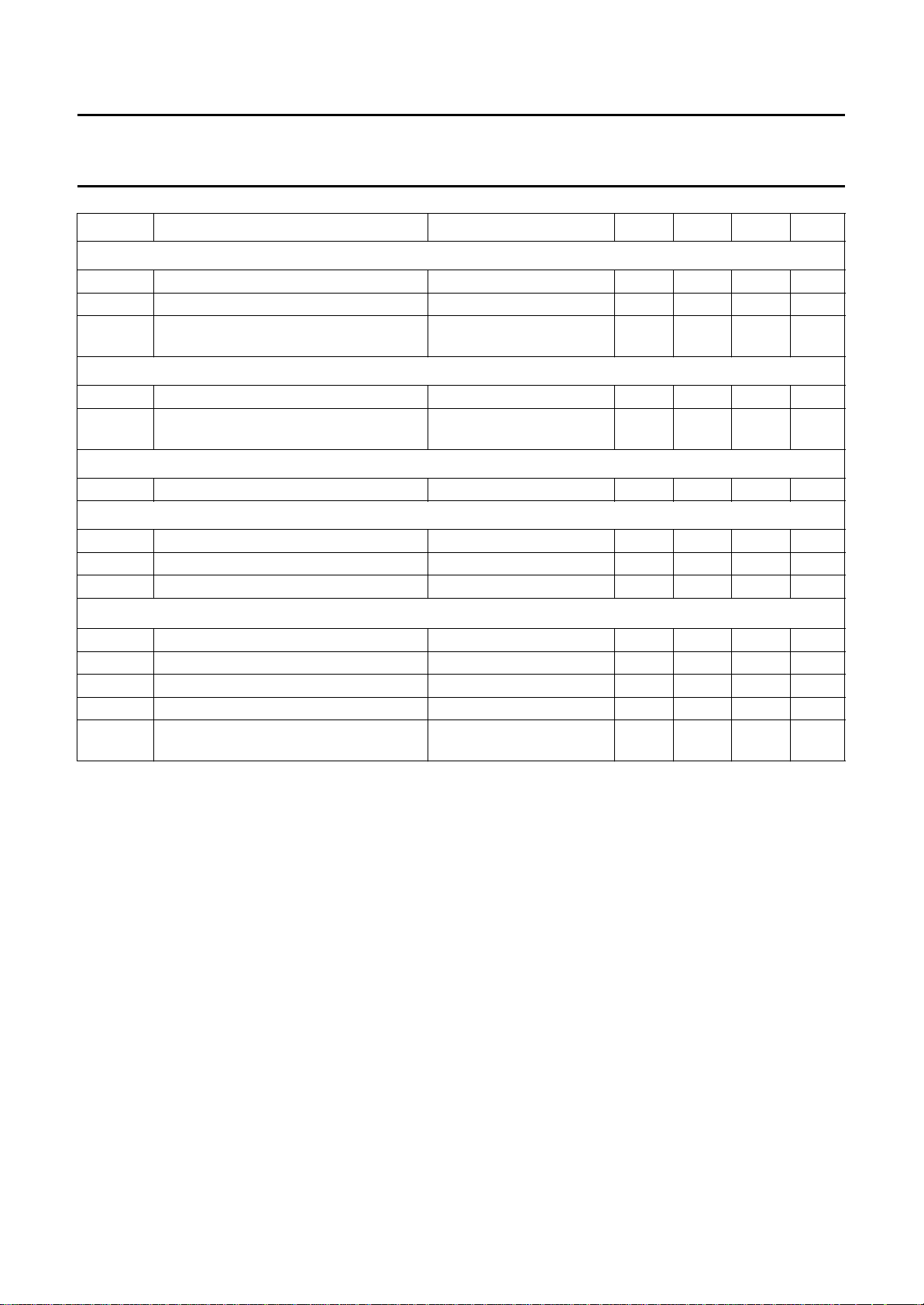
SYMBOL PARAMETER CONDITIONS MIN. TYP. MAX. UNIT
Charge pump output (CP)
I
8
V
7
I
OZ
Amplifier output (AMP)
G amplifier current gain V
V
7sat
Crystal oscillator characteristics (XTAL)
Z
9
Output Port characteristics (P0)
V
OL
I
OZ
I
14(max)
2
C-bus receiver characteristics (SDA and SCL)
I
V
IH
V
IL
I
IH
I
IL
V
o
output current −±100 −µA
output voltage in lock 1.5 − 2.5 V
OFF-state leakage current VCP= 2 V; T0 = 1; T1 = 1;
−−10 nA
T2 = 1
=2V; I
CP
output saturation voltage VCP= 0 V; T0 = 1; T1 = 0;
=10µA − 4000 −
AMP
− 140 200 mV
T2 = 1
oscillator input impedance −−−500 Ω
LOW level output voltage P0 = 1; I14=5mA − 150 400 mV
OFF-state leakage current P0 = 0; VDD= 5.5 V −−10 µA
maximum Port current P0 = 1 −−10 mA
HIGH level input voltage 3 − 5.5 V
LOW level input voltage 0 − 1.5 V
HIGH level input current VIH=5V; VDD=0or5V −−10 µA
LOW level input current VIL=0V; VDD=0or5V −10 −−µA
output voltage on SDA during acknowledge
−−0.4 V
pulse; IIL=3mA
Notes
1. Modulation depth when the video signal is between 560 and 1000 mV (peak-to-peak value) at pin 19. R17 = 120 kΩ
in the application.
2. For application information only.
3. Ratio between the CCIR 17 line bar amplitude (corresponding to the level difference between black and white;
see Fig.4 and the RMS value of the noise on a black line (line 22 or 335) measured on the video signal after
demodulation for PAL G standard. Measurement is unweighted, done between 200 kHz and 5 MHz.
4. Measured for PAL G standard on 4 first steps of CCIR 330 line, corresponding to a 5 step staircase with
300 mV (peak-to-peak value) chrominance carrier when the level between synchronization pulse and white is 1 V;
see Fig.5.
5. Measured with a spectrum analyzer with ‘peak hold’ function, applying a 500 mV (peak-to-peak value) sine wave at
the video input of the IC, with a frequency of 0.5, 2.0, 4.0 and 4.8 MHz. The reference is the value measured for
1.0 MHz.
6. Measured using CCIR 468-3 weighting filter and quasi-peak detection, with an audio frequency of 1 kHz and a
deviation of 50 kHz. Video signal is EBU colour bars of 500 mV (peak-to-peak value) on pin 19.
7. Measured in PAL G standard with no pre-emphasis on the audio input and no de-emphasis in the receiver. Audio
input level is adjusted for having a deviation of 25 kHz at 1 kHz audio frequency. Measurement is done for
frequencies between 50 Hz and 15 kHz, reference is the level measured for 1 kHz.
1995 Mar 21 12
Page 13
Philips Semiconductors Objective specification
I2C-bus programmable modulator for
TDA8722
negative video modulation and FM sound
8. Except for the harmonics of the RF oscillator frequency and for the combinations between the RF oscillator
frequency and the sound oscillator frequency (fRF+2fs, 2fRF+fs, etc.). This measurement includes the spurious at
the1⁄4fRF,1⁄2fRF and3⁄4fRF.
9. Corresponding to the harmonics of the video signal. Measured by putting a 1 MHz sine wave of
500 mV (peak-to-peak value) at the video input (pin 19) and checking the level at fRF+ 2 MHz, fRF+ 3 MHz, etc.
10. Measured with a 4.43 MHz sine wave of 350 mV (peak-to-peak value) at the video input. Measurement is the
difference between the level of the unmodulated picture carrier and the level of the spike appearing at the frequency
of the picture carrier plus 1.07 MHz. C17 = 15 pF in the application diagram of Fig.7.
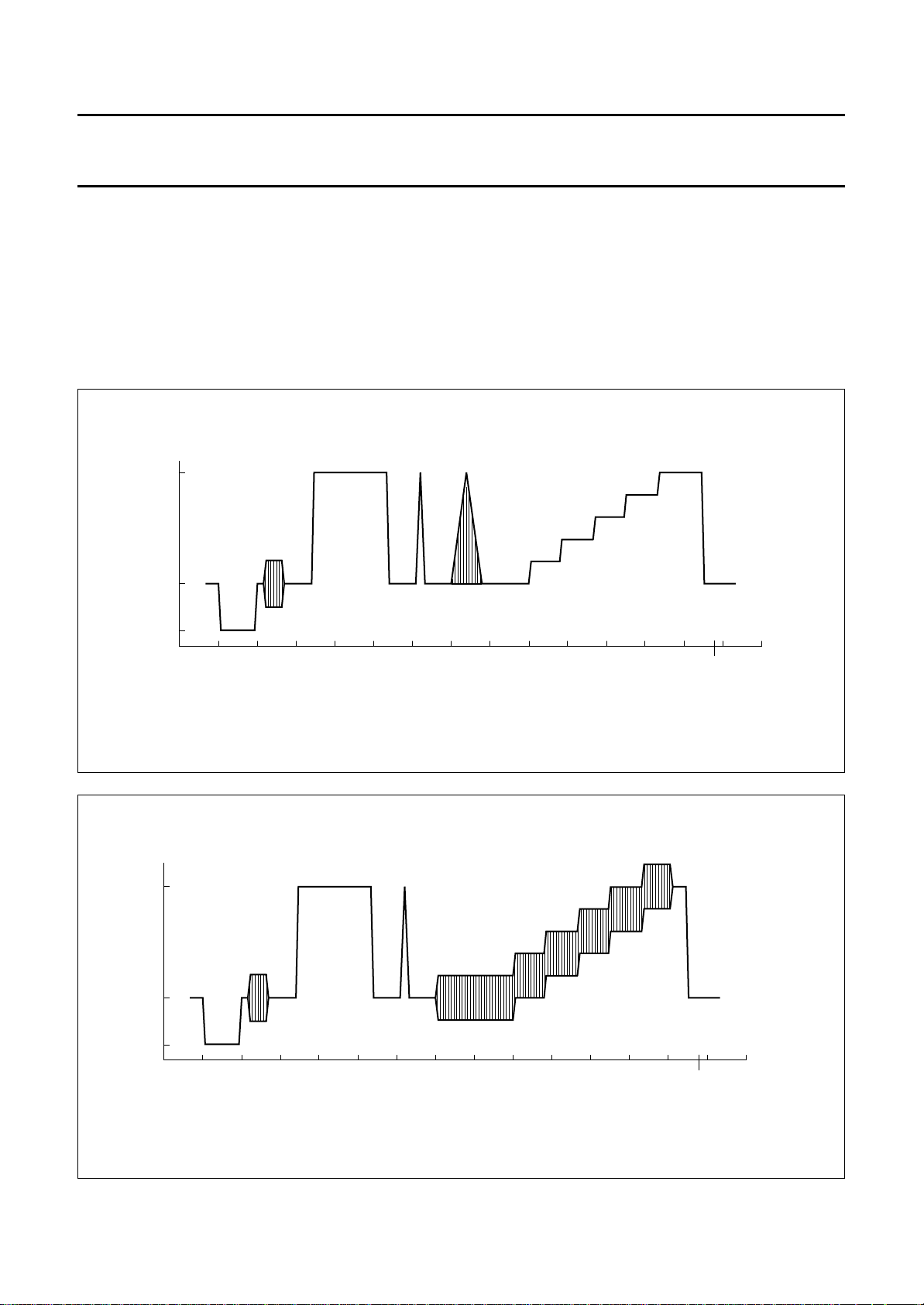
handbook, full pagewidth
1 V
0.3 V
MBE396
0 V
handbook, full pagewidth
1 V
0.3 V
0 V
010203040 50 60
t (µs)
Fig.4 CCIR insertion line N.17.
010203040 50 60
t (µs)
64
64
70
MBE397
70
1995 Mar 21 13
Fig.5 CCIR insertion line N.330.
Page 14
Philips Semiconductors Objective specification
I2C-bus programmable modulator for
negative video modulation and FM sound
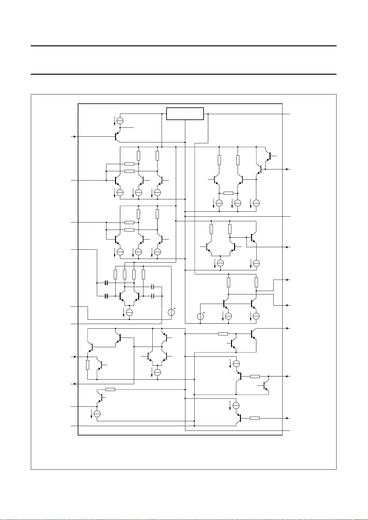
INTERNAL PIN CONFIGURATION
handbook, full pagewidth
AUDIO
SOSCA
SOSCB
1
2
3
VOLTAGE
REGULATOR
20
19
18
TDA8722
V
DDA
VIDEO
AGND
AMP
CP
4
5
6
7
8
9
10
UOSCB
OGND
UOSCA
XTAL
DGND
ESD protection components are not shown in the diagram.
17
16
15
14
13
12
11
MBE402
ADJUST
RFA
RFB
P0
SDA
SCL
V
DDD
1995 Mar 21 14
Fig.6 Pin equivalent circuit for each pin.
Page 15
Philips Semiconductors Objective specification
I2C-bus programmable modulator for
negative video modulation and FM sound
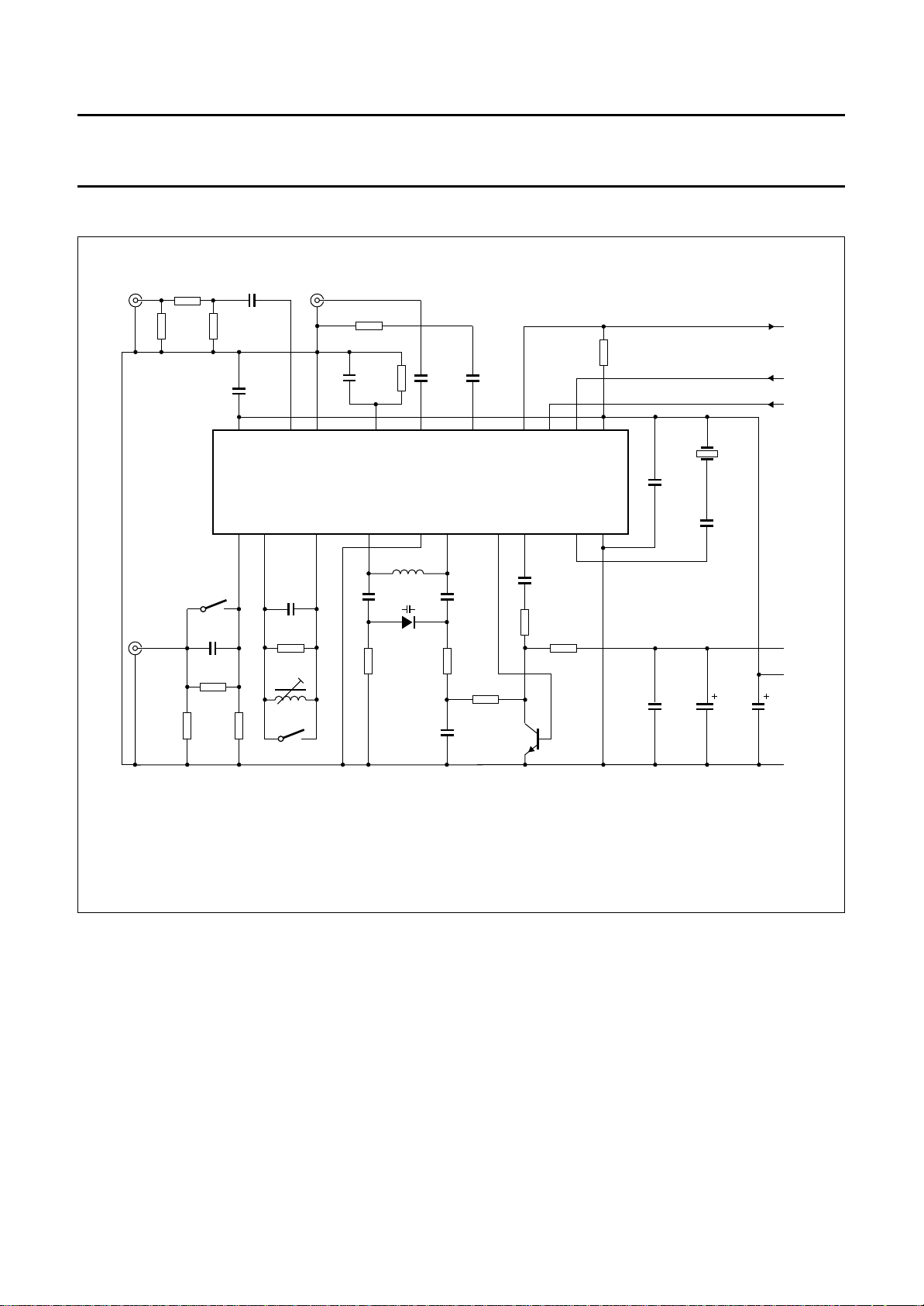
APPLICATION INFORMATION
C3
56 pF
R3
15 kΩ
(3)
L3
15 µH
K2
(4)
RF
75 Ω
15 pF
C17
R15
75 Ω
100 pF
R17
120 kΩ
C16
TDA8722
(2)
L5
33 pF 33 pF
C5 C6
D5
BB215
R5
22 kΩ
10 nF
C7
handbook, full pagewidth
VIDEO
AUDIO
R4
220 Ω
R20
470 Ω
R18
82 Ω
100 nF
C19
R19
470 Ω
100 nF
C20
20 1819 17 16 15 14 13 12 11
12 3 4 56 78 910
(1)
K1
C1
220 pF
R1
220 kΩ
R2
12 kΩ
R6
22 kΩ
100 pF
C15
R7
12 kΩ
T8
150 nF
C8
R8
12 kΩ
22 kΩ
BC547B
R9
1 kΩ
R14
Q9
10 nF
C11
C30
10 nF 2.2 µF
4 MHz
27 pF
C9
C31
MBE403
TDA8722
PORT
SCL
SDA
33 V
5 V
C21
2.2 µF
GND
(1) K1: switches the pre-emphasis filter on or off.
(2) L5: air coil; 1.5 turns; diameter of 2 mm.
(3) L3: to adjust the application to the right sound carrier frequency (5.5 MHz for PAL G).
(4) K2: Switches the FM sound oscillator on or off.
Fig.7 Reference measuring set-up.
1995 Mar 21 15
Page 16
Philips Semiconductors Objective specification
I2C-bus programmable modulator for
negative video modulation and FM sound
Application design
handbook, full pagewidth
VIDEO
82 Ω
AUDIO
R20
470 Ω
R18
100 nF
C19
R19
470 Ω
20 1819 17 16 15 14 13 12 11
12 3 4 56 78 910
C1
220 pF
R1
220 kΩ
R2
12 kΩ
100 nF
C20
RF
75 Ω
C3
56 pF
R3
15 kΩ
L3
15 µH
100 kΩ
RV1
15 pF
C17
R15
75 Ω
82 kΩ
(1)
R17
TDA8722
L5
33 pF 33 pF
C5 C6
D5
BB215
R5
22 kΩ
10 nF
100 pF
C7
C16
R6
22 kΩ
100 pF
C15
R7
12 kΩ
T8
150 nF
C8
R8
12 kΩ
22 kΩ
BC547B
R9
10 nF
C11
C30
10 nF
TDA8722
Q9
4 MHz
27 pF
C9
MBE405
PORT
SCL
SDA
5 V
33 V
GND
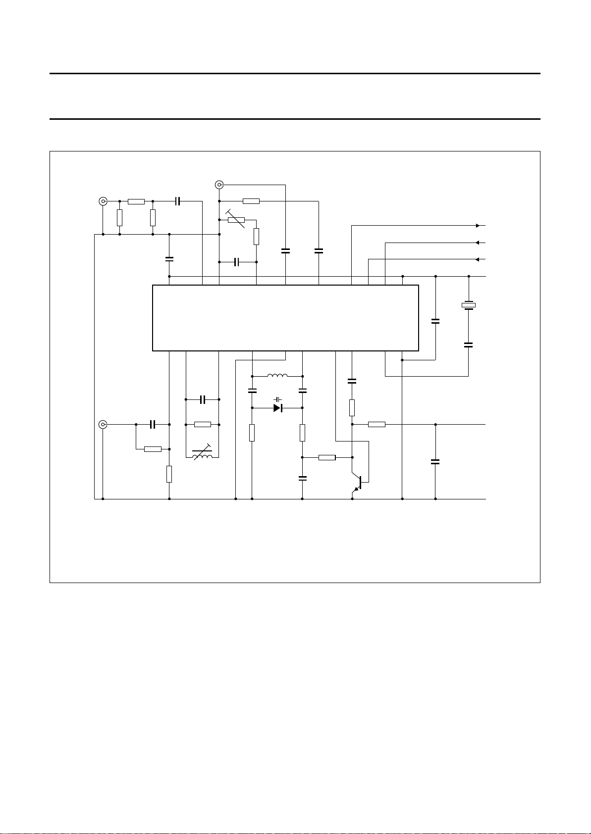
(1) RV1 allows fine adjustment of the modulation depth between 70 and 90%.
1995 Mar 21 16
Fig.8 Application using an asymmetrical output.
Page 17
Philips Semiconductors Objective specification
I2C-bus programmable modulator for
negative video modulation and FM sound
100 nF
C20
RF
75 Ω
C3
56 pF
R3
15 kΩ
L3
15 µH
120 kΩ
C17
15 pF
33 pF 33 pF
C5 C6
22 kΩ
64
1
R17
100 pF
C16
R15
300 Ω
TDA8722
L5
D5
BB215
R5
10 nF
C7
TR1
23
22 kΩ
handbook, full pagewidth
VIDEO
AUDIO
R20
470 Ω
R18
82 Ω
100 nF
C19
R19
470 Ω
20 1819 17 16 15 14 13 12 11
12 3 4 56 78 910
C1
220 pF
R1
220 kΩ
R2
12 kΩ
100 pF
R6
R7
12 kΩ
TOKO - B4F
617DB - 1010
C15
150 nF
T8
C8
R8
12 kΩ
22 kΩ
BC547B
R9
10 nF
C11
C30
10 nF
TDA8722
Q9
4 MHz
27 pF
C9
MBE404
PORT
SCL
SDA
5 V
33 V
GND
In the design of the application, it is highly recommended
to separate the part of the RF oscillator as much as
possible from the part of the RF outputs in order to avoid
parasitic coupling between these two parts.
A good solution is shielding the RF oscillator part to avoid
radiation from and to this part. The pin 5 (OGND) must be
connected to the shielding box and to ground.
RF outputs
For inexpensive applications, it is possible to use the IC
with an asymmetrical output (pins 15 or 16). In this event,
the unused output pin must be loaded with a load as
1995 Mar 21 17
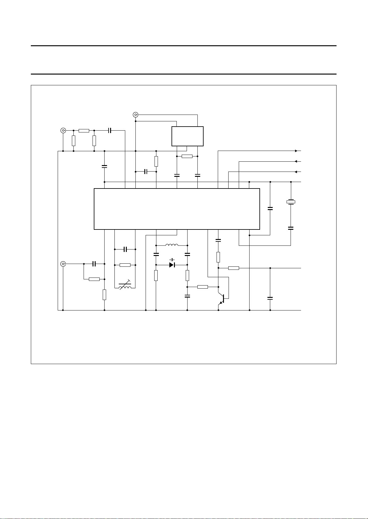
Fig.9 Application using a symmetrical output with a balun transformer.
similar as possible to the load connected to the used pin,
see Fig.8.
A good improvement in performance is obtained using a
1 : 4 symmetrical to asymmetrical transformer
(balun; balance-to-unbalance) connected between the two
outputs. In this event both outputs have their loads
matched. The level of the RF second harmonic, and the
spurious outside channel is decreasing. The parasitic
coupling between RF outputs and RF oscillator is also
reduced (see Fig.9).
Page 18
Philips Semiconductors Objective specification
I2C-bus programmable modulator for
negative video modulation and FM sound
Modulation depth
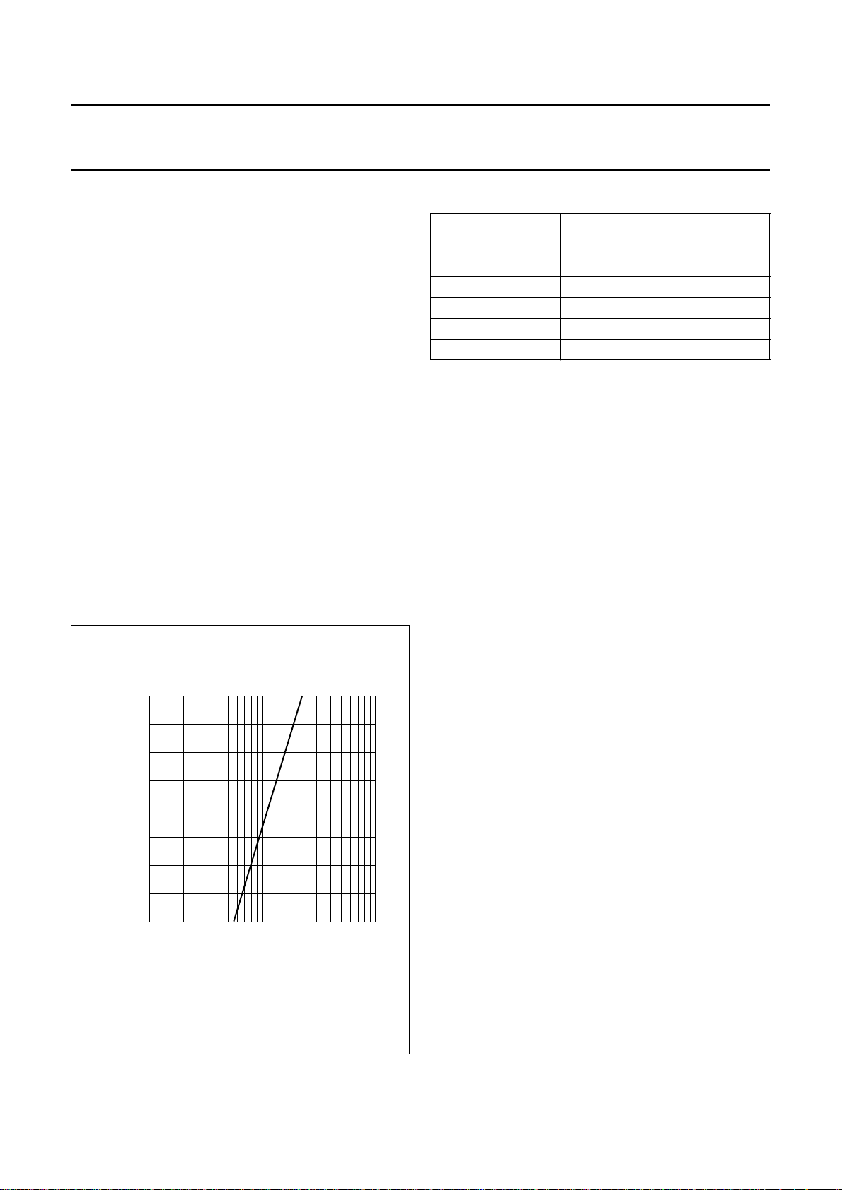
With 500 mV (peak-to-peak value) video input signal, the
wanted modulation depth must be set by the value of R17
(resistor between pin 17 and ground) as shown Fig.10. For
a good accuracy, it is recommended to use a 1% type
resistor.
It is also possible to use an adjustable resistor, see Fig.8.
Depending on the layout of the PCB, it may be necessary
to slightly change the value of R17 from the one given in
Fig.10 to get the wanted modulation depth.
Sound oscillator design
The frequency of the sound subcarrier is fixed by the tank
circuit connected between pins 2 and 3. This frequency
can be adjusted between 4.5 and 6.5 MHz covering all
existing standards in the world.
The damping resistor R3 between pins 2 and 3 is
necessary to decrease the quality factor of the tank circuit
allowing the frequency to be modulated by the audio
signal. The value of this resistor is calculated for several
Q factor ranges of the coil for a sound frequency of
5.5 MHz (see Table 7).
TDA8722
Table 7 Value of resistor for several Q factor ranges
COIL QUALITY
FACTOR
30 to 40 82 to 33
40 to 50 33 to 27
50 to 60 27 to 22
60 to 80 22 to 18
80 to >100 18 to 15
The use of a coil with a quality factor <30 may result in a
non operating oscillator. For safety, it is recommended to
use a coil with a quality factor ≥50.
Picture-to-sound ratio
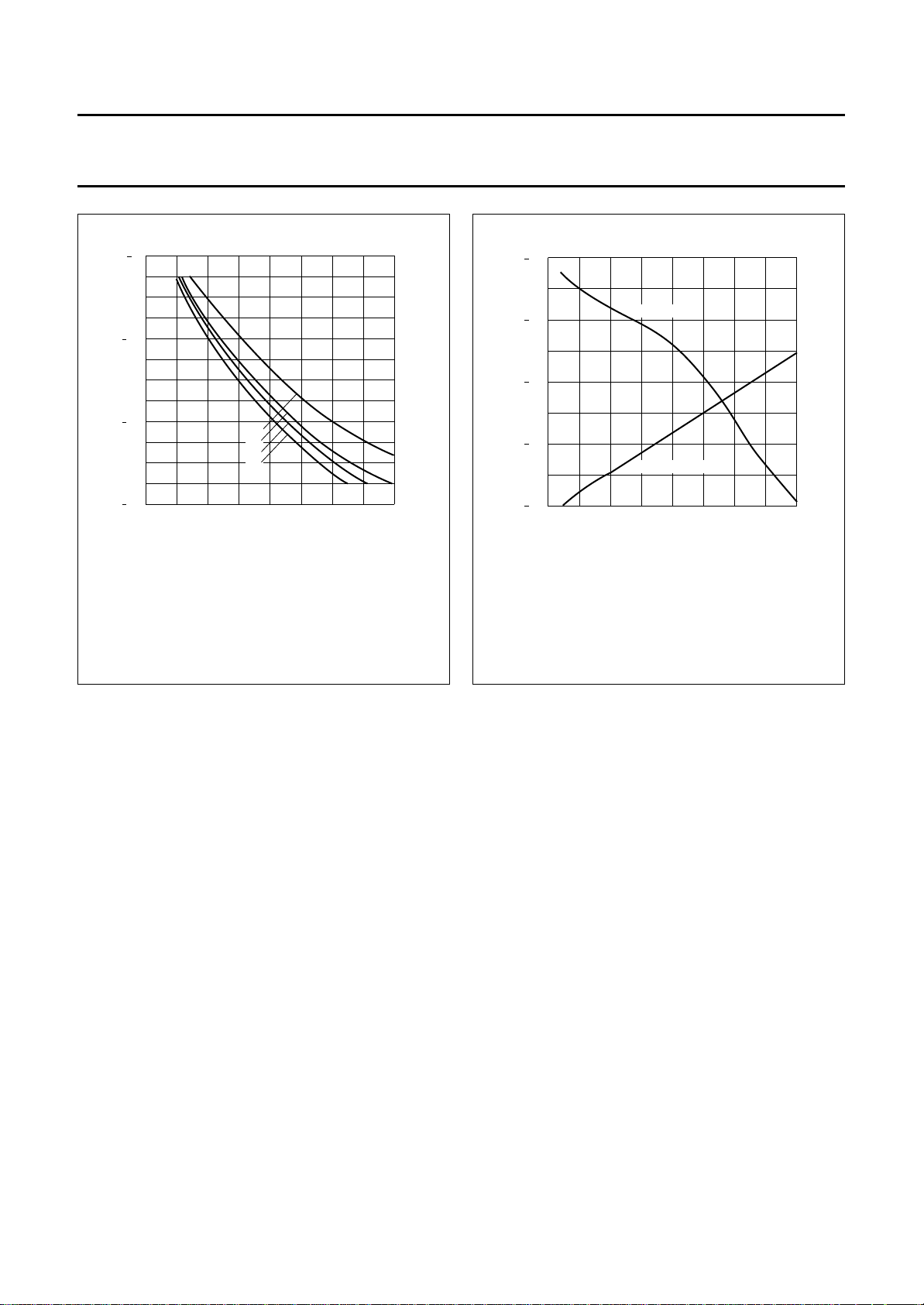
The picture-to-sound ratio can be adjusted in the
application by changing the value of C17 (capacitor
between pin 17 and ground); see Fig.11.
Figure 11 shows us that the picture-to-sound ratio will
change for a constant value of C17 when the sound
subcarrier frequency will change.
RF harmonics
PROPOSED VALUE FOR R3
(kΩ)
100
handbook, halfpage
modulation
depth
(%)
90
80
70
60
10
2
10
R17 (kΩ)
MBE398
10
Fig.10 Typical modulation depth as a function of
the value of R17.
This IC has been designed to have the lowest level of
unwanted RF harmonics at the frequencies where these
are the hardest to be filtered out, especially for the second
harmonic of the RF carrier at the lowest frequencies of the
UHF band.
The level of the second and third RF harmonic is shown in
Fig.12 for an asymmetrical application. This chart gives a
typical value while the level of these harmonics can vary
depending on the design of the application.
It is possible to reduce the level of the second harmonic by
using a wide band transformer at the output of the IC and
create a symmetrical application (see Fig.9).
To reduce the out-of-band harmonics and especially the
third one, it is necessary to use a low-pass filter at the
output of the IC.
3
1995 Mar 21 18
Page 19
Philips Semiconductors Objective specification
I2C-bus programmable modulator for
negative video modulation and FM sound
30
MBE399
C17 (pF)
handbook, halfpage
8
P/S
(dB)
12
16
20
01020 40
R17 = 120 kΩ.
(1) 4.5 MHz.
(2) 5.5 MHz.
(3) 6.0 MHz.
(4) 6.5 MHz.
(1)
(2)
(3)
(4)
14
handbook, halfpage
RF
harmonics
(dBc)
18
22
26
30
450 550
third harmonic
second harmonic
650 750 850
TDA8722
MBE400
RF (MHz)
Fig.11 Typical picture-to-sound ratio as a function
of the value of C17.
VHF operation
This IC can operate on frequencies as low as 200 MHz
(and especially for VHF 3 band) provided the impedance
of the tuned circuit between pins 4 and 6 is >1 kΩ.
NICAM and stereo
Because of the fact that the ADJUST pin (pin 17) is an
access point to the RF mixer, it is possible to use this pin
to inject an external modulated subcarrier into the IC.
This is especially interesting when it is necessary to
transmit a second frequency modulated audio subcarrier
for stereo sound (f = 5.72 MHz) or a NICAM QPSK
modulated carrier for digital audio transmission
(f = 5.85 or 6.552 MHz).
The incoming signal must be externally modulated either
in FM with the desired signal corresponding to PAL B/G
specification for stereo sound transmission, or in QPSK in
accordance with the NICAM transmission system.
Fig.12 Typical level of RF harmonics for an
asymmetrical application.
The input impedance on pin 17 is approximately 3500 Ω,
the incoming signal must be capacitive coupled, the
resistor R17 between pin 17 and ground must remain to
adjust the modulation depth, the capacitor C17 between
pin 17 and ground may be changed depending on the
capacitance brought on by the incoming network. If this
capacitance is large, it is possible to remove C17.
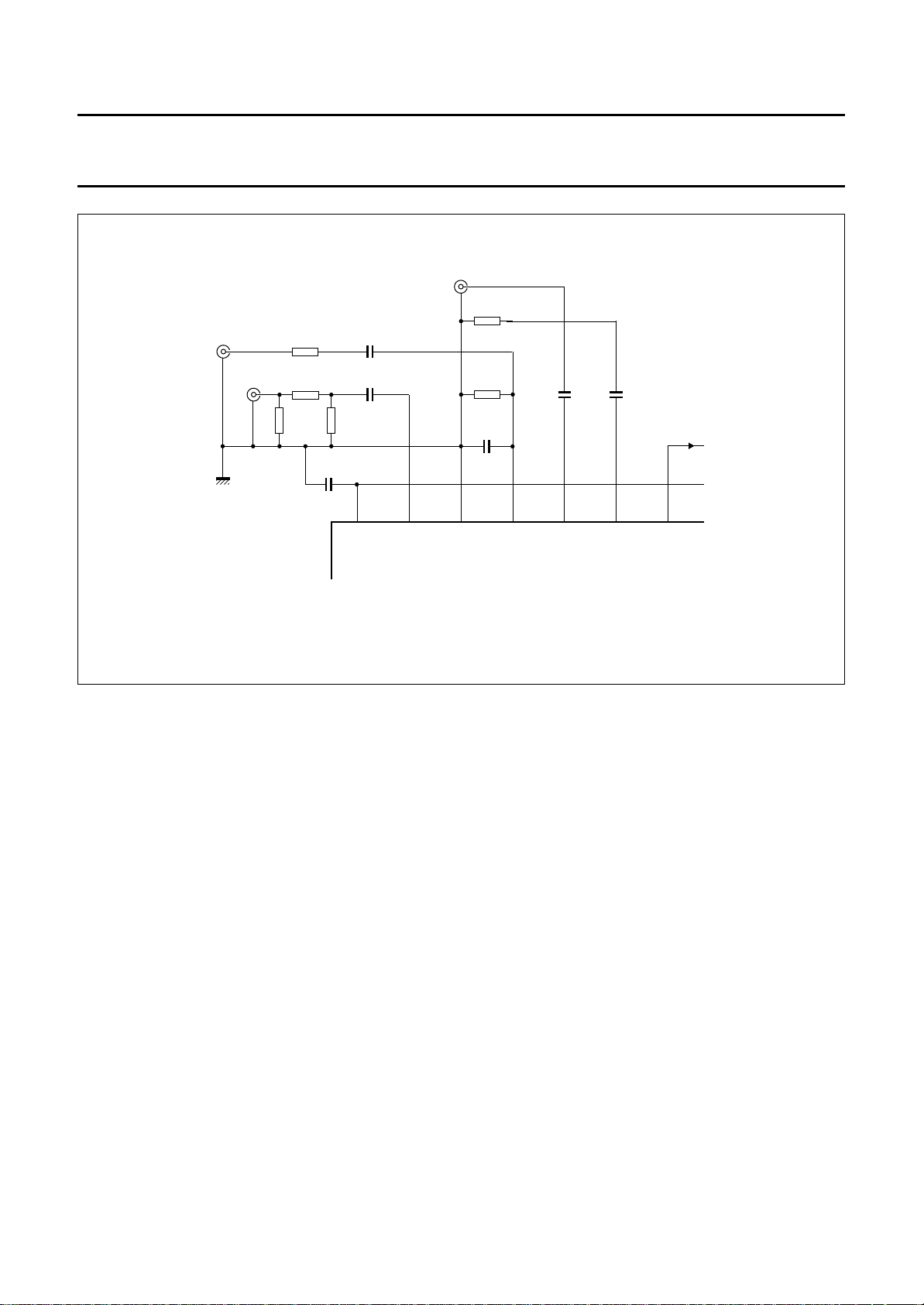
Figure 13 shows a possible application for injecting such
kind of signal into the modulator IC.
Following this application, to get a picture-to-second
sound carrier ratio of −20 dB, it is necessary to apply a
level of approximately 800 mV (peak-to-peak value) at the
second carrier input, when the picture-to-first sound carrier
ratio is approximately −13 dB.
In addition, the internal FM sound modulator can be
switched off by short-circuiting pins 2 and 3.
1995 Mar 21 19
Page 20
Philips Semiconductors Objective specification
I2C-bus programmable modulator for
negative video modulation and FM sound
RF 75 Ω
handbook, full pagewidth
SECOND
CARRIER
VIDEO
R21
10 kΩ
R20
470 Ω
R18
82 Ω
10 pF
C21
100 nF
C19
R19
470 Ω
100 nF
C20
20 1819 17 16 15 14
R15
75 Ω
R17
120 kΩ
C17
100 pF
C16
TDA8722
TDA8722
100 pF
C15
PORT
MGC419
Fig.13 Possible application for a second sound subcarrier.
1995 Mar 21 20
Page 21
Philips Semiconductors Objective specification
I2C-bus programmable modulator for
negative video modulation and FM sound
PACKAGE OUTLINES
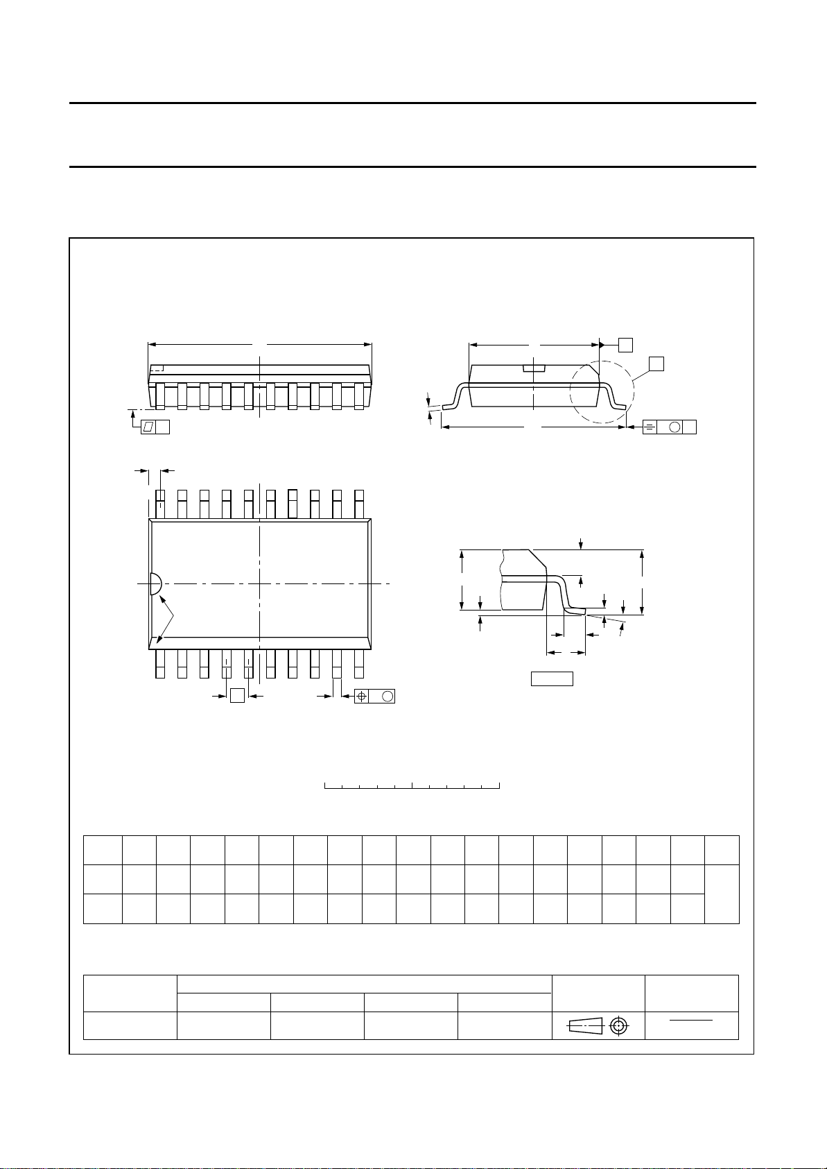
SO20: plastic small outline package; 20 leads; body width 7.5 mm
D
c
y
Z
20
11
TDA8722
SOT163-1
E
H
E
A
X
v
M
A
pin 1 index
1
e
0 5 10 mm
DIMENSIONS (inch dimensions are derived from the original mm dimensions)
mm
A
max.
2.65
0.10
A
1
0.30
0.10
0.012
0.004
A2A
2.45
2.25
0.096
0.089
0.25
0.01
b
0.49
0.36
p
cD
0.32
0.23
0.013
0.009
3
0.019
0.014
UNIT
inches
Note
1. Plastic or metal protrusions of 0.15 mm maximum per side are not included.
10
w
b
p
13.0
12.6
0.51
0.49
M
scale
(1)E(1) (1)
0.30
0.29
eHELLpQ
7.6
1.27
7.4
0.050
10.65
10.00
0.42
0.39
Q
A
2
A
1
1.4
0.055
1.1
0.4
0.043
0.016
detail X
1.1
1.0
0.043
0.039
(A )
L
p
L
0.25
0.01
A
3
θ
0.25 0.1
0.01
ywv θ
Z
0.9
0.4
8
0.004
0.035
0.016
0
o
o
OUTLINE
VERSION
SOT163-1
1995 Mar 21 21
REFERENCES
IEC JEDEC EIAJ
075E04 MS-013AC
EUROPEAN
PROJECTION
ISSUE DATE
92-11-17
95-01-24
Page 22
Philips Semiconductors Objective specification
I2C-bus programmable modulator for
negative video modulation and FM sound
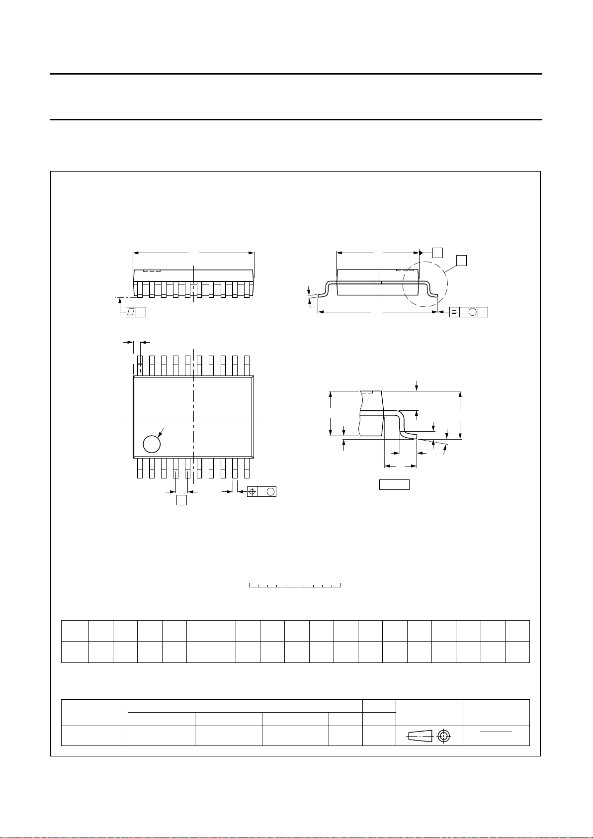
SSOP20: plastic shrink small outline package; 20 leads; body width 4.4 mm
20
D
c
y
Z
11
E
H
E
TDA8722
SOT266-1
A
X
v
M
A
pin 1 index
110
w
b
e
DIMENSIONS (mm are the original dimensions)
mm
A
max.
1.5
0.1501.4
1.2
0.25
b
3
p
0.32
0.20
UNIT A1A2A
Note
1. Plastic or metal protrusions of 0.20 mm maximum per side are not included.
p
cD
0.20
0.13
M
0 2.5 5 mm
scale
(1)E(1)
6.6
6.4
eHELLpQZywv θ
4.5
0.65 1.0 0.2
4.3
6.6
6.2
Q
A
2
A
1
detail X
0.65
0.75
0.45
0.45
(A )
L
p
L
A
3
θ
0.13 0.1
0.48
0.18
(1)
o
10
o
0
OUTLINE
VERSION
SOT266-1
1995 Mar 21 22
REFERENCES
IEC JEDEC EIAJ
EUROPEAN
PROJECTION
ISSUE DATE
90-04-05
95-02-25
Page 23

Philips Semiconductors Objective specification
I2C-bus programmable modulator for
negative video modulation and FM sound
SOLDERING
Plastic small outline packages
YWAVE
B
During placement and before soldering, the component
must be fixed with a droplet of adhesive. After curing the
adhesive, the component can be soldered. The adhesive
can be applied by screen printing, pin transfer or syringe
dispensing.
Maximum permissible solder temperature is 260 °C, and
maximum duration of package immersion in solder bath is
10 s, if allowed to cool to less than 150 °C within 6 s.
Typical dwell time is 4 s at 250 °C.
A modified wave soldering technique is recommended
using two solder waves (dual-wave), in which a turbulent
wave with high upward pressure is followed by a smooth
laminar wave. Using a mildly-activated flux eliminates the
need for removal of corrosive residues in most
applications.
Y SOLDER PASTE REFLOW
B
TDA8722
Several techniques exist for reflowing; for example,
thermal conduction by heated belt, infrared, and
vapour-phase reflow. Dwell times vary between 50 and
300 s according to method. Typical reflow temperatures
range from 215 to 250 °C.
Preheating is necessary to dry the paste and evaporate
the binding agent. Preheating duration: 45 min at 45 °C.
R
EPAIRING SOLDERED JOINTS (BY HAND-HELD SOLDERING
IRON OR PULSE
Fix the component by first soldering two, diagonally
opposite, end pins. Apply the heating tool to the flat part of
the pin only. Contact time must be limited to 10 s at up to
300 °C. When using proper tools, all other pins can be
soldered in one operation within 2 to 5 s at between 270
and 320 °C. (Pulse-heated soldering is not recommended
for SO packages.)
For pulse-heated solder tool (resistance) soldering of VSO
packages, solder is applied to the substrate by dipping or
by an extra thick tin/lead plating before package
placement.
-HEATED SOLDER TOOL)
Reflow soldering requires the solder paste (a suspension
of fine solder particles, flux and binding agent) to be
applied to the substrate by screen printing, stencilling or
pressure-syringe dispensing before device placement.
1995 Mar 21 23
Page 24

Philips Semiconductors Objective specification
I2C-bus programmable modulator for
TDA8722
negative video modulation and FM sound
DEFINITIONS
Data sheet status
Objective specification This data sheet contains target or goal specifications for product development.
Preliminary specification This data sheet contains preliminary data; supplementary data may be published later.
Product specification This data sheet contains final product specifications.
Limiting values
Limiting values given are in accordance with the Absolute Maximum Rating System (IEC 134). Stress above one or
more of the limiting values may cause permanent damage to the device. These are stress ratings only and operation
of the device at these or at any other conditions above those given in the Characteristics sections of the specification
is not implied. Exposure to limiting values for extended periods may affect device reliability.
Application information
Where application information is given, it is advisory and does not form part of the specification.
LIFE SUPPORT APPLICATIONS
These products are not designed for use in life support appliances, devices, or systems where malfunction of these
products can reasonably be expected to result in personal injury. Philips customers using or selling these products for
use in such applications do so at their own risk and agree to fully indemnify Philips for any damages resulting from such
improper use or sale.
PURCHASE OF PHILIPS I
Purchase of Philips I
components in the I2C system provided the system conforms to the I2C specification defined by
Philips. This specification can be ordered using the code 9398 393 40011.
2
C COMPONENTS
2
C components conveys a license under the Philips’ I2C patent to use the
1995 Mar 21 24
 Loading...