

Page 1

DATA SH EET
Product specification
Supersedes data of June 1994
File under Integrated Circuits, IC02
1996 Nov 26
INTEGRATED CIRCUITS
TDA8708B
Video analog input interface
Page 2
1996 Nov 26 2
Philips Semiconductors Product specification
Video analog input interface TDA8708B
FEATURES
• 8-bit resolution
• Sampling rate up to 32 MHz
• Binary or two’s complement 3-state TTL outputs
• TTL-compatible digital inputs and outputs
• Internal reference voltage regulator
• Power dissipation of 365 mW (typical)
• Input selector circuit (one out of three video inputs)
• Clamp and Automatic Gain Control (AGC) functions for
CVBS and Y signals
• No sample-and-hold circuit required
• The TDA8708B has no white peak control in mode 2
whereas the TDA8708A has control in modes 1 and 2
• In-range output (not TTL levels).
APPLICATIONS
• Video signal decoding
• Scrambled TV (encoding and decoding)
• Digital picture processing
• Frame grabbing.
GENERAL DESCRIPTION
The TDA8708B is an analog input interface for video signal
processing. It includes a video amplifier with clamp and
gain control, an 8-bit Analog-to-Digital Converter (ADC)
with a sampling rate of 32 MHz and an input selector.
QUICK REFERENCE DATA
ORDERING INFORMATION
SYMBOL PARAMETER MIN. TYP. MAX. UNIT
V
CCA
analog supply voltage 4.5 5.0 5.5 V
V
CCD
digital supply voltage 4.5 5.0 5.5 V
V
CCO
TTL output supply voltage 4.2 5.0 5.5 V
I
CCA
analog supply current − 37 45 mA
I
CCD
digital supply current − 24 30 mA
I
CCO
TTL output supply current − 12 16 mA
ILE DC integral linearity error −−±1 LSB
DLE DC differential linearity error −−±0.5 LSB
f
clk(max)
maximum clock frequency 30 32 − MHz
B maximum −3 dB bandwidth (AGC amplifier) 12 18 − MHz
P
tot
total power dissipation − 365 500 mW
TYPE NUMBER
PACKAGE
NAME DESCRIPTION VERSION
TDA8708BT SO28 plastic small outline package; 28 leads; body width 7.5 mm SOT136-1
Page 3
1996 Nov 26 3
Philips Semiconductors Product specification
Video analog input interface TDA8708B
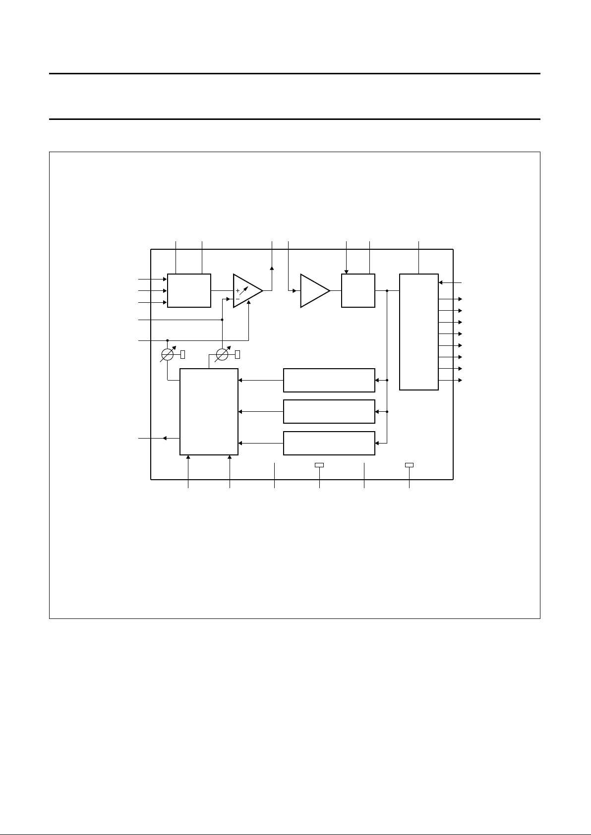
BLOCK DIAGRAM
Fig.1 Block diagram.
handbook, full pagewidth
MSA672
TTL
OUTPUTS
9
1
2
3
4
10
11
12
13
output format/
chip enable
(3-state input)
D7
D6
D5
D4
D3
D2
D1
D0
8 - bit
ADC
AMP.
VIDEO
AMPLIFIER
INPUT
SELECTOR
16
17
18
19 2014 15
video input
selection bit 0
video input
selection bit 1
analog
voltage
output
ADC
input
clock
input
decoupling
input
521 7
video input 0
video input 1
video input 2
clamp capacitor
connection
AGC capacitor
connection
24
25
AGC &
CLAMP
LOGIC
&
MODE
SELECTION
PEAK LEVEL
DIGITAL COMPARATOR
27 26
sync level
sync pulse
black level
sync pulse
6
digital
ground
8 22
analog
ground
23
TDA8708B
28
BLACK LEVEL
DIGITAL COMPARATOR
SYNC LEVEL
DIGITAL COMPARATOR
in-range
output
TTL outputs V (+ 5 V)
digital V
CCD
(+ 5 V)
analog V
CCA
(+ 5 V)
CCO
Page 4
1996 Nov 26 4
Philips Semiconductors Product specification
Video analog input interface TDA8708B
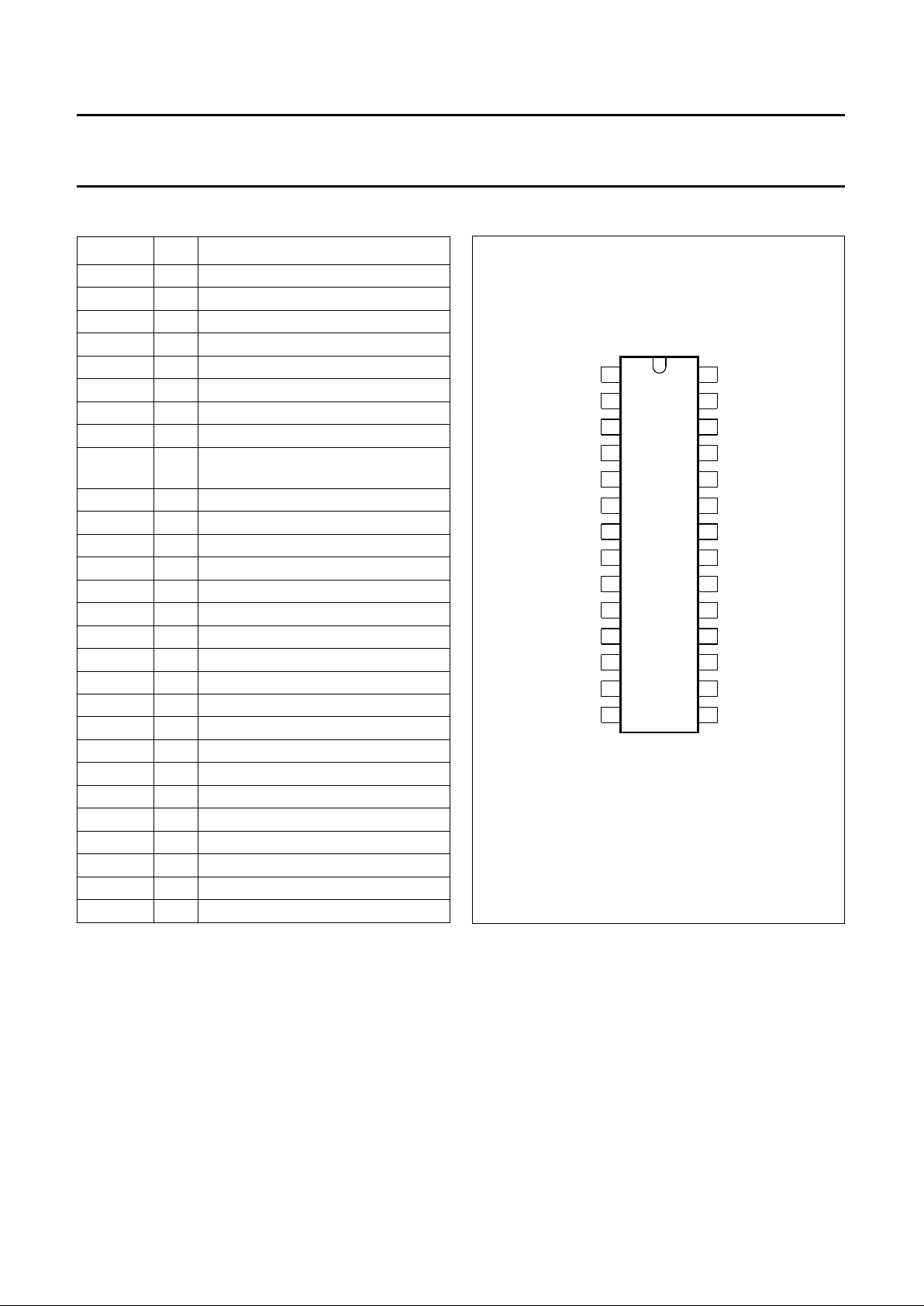
PINNING
SYMBOL PIN DESCRIPTION
D7 1 data output; bit 7 (MSB)
D6 2 data output; bit 6
D5 3 data output; bit 5
D4 4 data output; bit 4
CLK 5 clock input
V
CCD
6 digital supply voltage (+5 V)
V
CCO
7 TTL outputs supply voltage (+5 V)
DGND 8 digital ground
OF 9 output format/chip enable
(3-state input)
D3 10 data output; bit 3
D2 11 data output; bit 2
D1 12 data output; bit 1
D0 13 data output; bit 0 (LSB)
I0 14 video input selection bit 0
I1 15 video input selection bit 1
VIN0 16 video input 0
VIN1 17 video input 1
VIN2 18 video input 2
ANOUT 19 analog voltage output
ADCIN 20 analog-to-digital converter input
DEC 21 decoupling input
V
CCA
22 analog supply voltage (+5 V)
AGND 23 analog ground
CLAMP 24 clamp capacitor connection
AGC 25 AGC capacitor connection
GATE B 26 black level synchronization pulse
GATE A 27 sync level synchronization pulse
IR 28 in-range output
Fig.2 Pin configuration.
1
2
3
4
5
6
7
8
9
10
11
12
13
28
27
26
25
24
23
22
21
20
19
18
17
16
1514
TDA8708B
D7
D6
D5
D4
CLK
V
CCD
V
CCO
DGND
OF
D3
D2
D1
D0
I0
ADCIN
ANOUT
VIN2
VIN1
VIN0
I1
GATE B
AGC
CLAMP
AGND
V
CCA
DEC
IR
GATE A
MSA671
Page 5
1996 Nov 26 5
Philips Semiconductors Product specification
Video analog input interface TDA8708B
FUNCTIONAL DESCRIPTION
The TDA8708B provides a simple interface for decoding
video signals.
The TDA8708B operates in configuration mode 1
(see Fig.4) when the video signals are weak (i.e. when the
gain of the AGC amplifier has not yet reached its optimum
value). This enables a fast recovery of the synchronization
pulses in the decoder circuit. When the pulses at the
GATE A and GATE B inputs become distinct (GATE A and
GATE B pulses are synchronization pulses occurring
during the sync period and rear porch respectively) the
TDA8708B automatically switches to configuration mode 2
(see Fig.5).
When the TDA8708B is in configuration mode 1, the gain
of the AGC amplifier will be roughly adjusted (sync level to
a digital output level of 0 and the peak level to a digital
output level of 255).
In configuration mode 2 the digital output of the ADC is
compared to internal digital reference levels.
The voltage across the capacitor connected to the AGC
pin controls the gain of the video amplifier. This is the gain
control loop.
The sync level comparator is active during a positive-going
pulse at the GATE A input. This means that the sync pulse
of the composite video signal is used as an amplitude
reference. The bottom of the sync pulse is adjusted to
obtain a digital output of logic 0 at the converter output.
As the black level is at digital level 64, the sync pulse will
have a digital amplitude of 64 LSBs.
The use of nominal signals will prevent the output from
exceeding a digital code of 213.
The clamp level control is accomplished by using the same
techniques as used for the gain control. The black-level
digital comparator is active during a positive-going pulse at
the GATE B input. The clamp capacitor will be charged or
discharged to adjust the digital output to code 64.
LIMITING VALUES
In accordance with the Absolute Maximum Rating System (IEC 134).
THERMAL CHARACTERISTICS
SYMBOL PARAMETER MIN. MAX. UNIT
V
CCA
analog supply voltage −0.3 +7.0 V
V
CCD
digital supply voltage −0.3 +7.0 V
V
CCO
TTL output supply voltage −0.3 +7.0 V
∆V
CC
supply voltage differences:
V
CCA
− V
CCD
−1.0 +1.0 V
V
CCO
− V
CCD
−1.0 +1.0 V
V
CCA
− V
CCO
−1.0 +1.0 V
V
I
input voltage −0.3 V
CCA
V
I
O
output current 0 +10 mA
T
stg
storage temperature −55 +150 °C
T
amb
operating ambient temperature 0 +70 °C
T
j
junction temperature 0 +125 °C
SYMBOL PARAMETER VALUE UNIT
R
th j-a
thermal resistance from junction to ambient in free air 70 K/W
Page 6
1996 Nov 26 6
Philips Semiconductors Product specification
Video analog input interface TDA8708B
CHARACTERISTICS
V
CCA=V22
to V23= 4.5 to 5.5 V; V
CCD=V6
to V8= 4.5 to 5.5 V; V
CCO=V7
to V8= 4.2 to 5.5 V; AGND and DGND
shorted together; V
CCA
to V
CCD
= −0.5 to +0.5 V; V
CCO
to V
CCD
= −0.5 to +0.5 V; V
CCA
to V
CCO
= −0.5 to +0.5 V;
T
amb
= 0 to +70 °C; typical readings taken at V
CCA=VCCD=VCCO
= 5 V and T
amb
=25°C; unless otherwise specified.
SYMBOL PARAMETER CONDITIONS MIN. TYP. MAX. UNIT
Supplies
V
CCA
analog supply voltage 4.5 5.0 5.5 V
V
CCD
digital supply voltage 4.5 5.0 5.5 V
V
CCO
TTL output supply voltage 4.2 5.0 5.5 V
I
CCA
analog supply current − 37 45 mA
I
CCD
digital supply current − 24 30 mA
I
CCO
TTL output supply current TTL load (see Fig.8) − 12 16 mA
Video amplifier inputs
VIN0
TO VIN2 INPUTS
V
I(p-p)
input voltage (peak-to-peak value) AGC load with external
capacitor; note 1
0.6 − 1.5 V
Z
i
input impedance fi= 6 MHz 10 20 − kΩ
C
i
input capacitance fi= 6 MHz − 1 − pF
I0 AND I1 TTL INPUTS (see Table 1)
V
IL
LOW level input voltage 0 − 0.8 V
V
IH
HIGH level input voltage 2.0 − V
CCD
V
I
IL
LOW level input current VI= 0.4 V −400 −−µA
I
IH
HIGH level input current VI= 2.7 V −− 20 µA
GATE A AND GATE B TTL INPUTS (see Figs 4 and 5)
V
IL
LOW level input voltage 0 − 0.8 V
V
IH
HIGH level input voltage 2.0 − V
CCD
V
I
IL
LOW level input current VI= 0.4 V −400 −−µA
I
IH
HIGH level input current VI= 2.7 V −− 20 µA
t
W
pulse width see Fig.5 2 −−µs
AGC INPUT (PIN 25)
V
25(min)
AGC voltage for minimum gain − 2.8 − V
V
25(max)
AGC voltage for maximum gain − 4.0 − V
AGC output current see Table 2
CLAMP
INPUT (PIN 24)
V
24
clamp voltage for code 128 output − 3.5 − V
I
24
clamp output current see Table 3
Page 7
1996 Nov 26 7
Philips Semiconductors Product specification
Video analog input interface TDA8708B
Video amplifier outputs
ANOUT OUTPUT (PIN 19)
V
19(p-p)
AC output voltage
(peak-to-peak value)
V
VIN
= 1.33 V (p-p);
V25= 3.6 V
− 1.33 − V
I
19
internal current source RL= ∞ 2.0 2.5 − mA
I
O(p-p)
output current driven by the load V
ANOUT
= 1.33 V (p-p);
note 2
−− 1.0 mA
V
19
DC output voltage for black level note 3 − V
CCA
− 2.24 − V
Z
19
output impedance − 20 −Ω
Video amplifier dynamic characteristics
α
ct
crosstalk between VIN inputs V
CCA
= 4.75 to 5.25 V −−50 −45 dB
G
diff
differential gain V
VIN
= 1.33 V (p-p);
V25= 3.6 V
− 2 − %
ϕ
diff
differential phase V
VIN
= 1.33 V (p-p);
V25= 3.6 V
− 0.8 − deg
B −3 dB bandwidth 12 −−MHz
S/N signal-to-noise ratio note 4 60 −−dB
SVRR1 supply voltage ripple rejection note 5 − 45 − dB
∆G gain range see Fig.10 −4.5 − +6.0 dB
G
stab
gain stability as a function of supply
voltage and temperature
see Fig.10 −− 5%
Analog-to-digital converter inputs
CLK
INPUT (PIN 5)
V
IL
LOW level input voltage 0 − 0.8 V
V
IH
HIGH level input voltage 2.0 − V
CCD
V
I
IL
LOW level input current V
clk
= 0.4 V −400 −−µA
I
IH
HIGH level input current V
clk
= 2.7 V −− 100 µA
|Z
i
| input impedance f
clk
= 10 MHz − 4 − kΩ
C
I
input capacitance f
clk
= 10 MHz − 4.5 − pF
OF INPUT (3-STATE; see Table 4)
V
IL
LOW level input voltage 0 − 0.2 V
V
IH
HIGH level input voltage 2.6 − V
CCD
V
V
9
input voltage in high impedance state − 1.15 − V
I
IL
LOW level input current −370 −300 −µA
I
IH
HIGH level input current − 300 450 µA
SYMBOL PARAMETER CONDITIONS MIN. TYP. MAX. UNIT
Page 8
1996 Nov 26 8
Philips Semiconductors Product specification
Video analog input interface TDA8708B
ADCIN INPUT (PIN 20; see Table 5)
V
20
input voltage digital output = 00 − V
CCA
− 2.42 − V
V
20
input voltage digital output = 255 − V
CCA
− 1.41 − V
V
20(p-p)
input voltage amplitude
(peak-to-peak value)
− 1.0 − V
I
20
input current − 1.0 10 µA
Z
i
input impedance fi= 6 MHz − 50 − MΩ
C
i
input capacitance fi= 6 MHz − 1 − pF
Analog-to-digital converter outputs
IR
OUTPUT (PIN 28)
V
OL
LOW level output voltage −− 1.7 V
V
OH
HIGH level output voltage 1.9 −−V
I
O
output current −500 −−µA
DIGITAL OUTPUTS D0 TO D7
V
OL
LOW level output voltage IOL= 2 mA 0 − 0.6 V
V
OH
HIGH level output voltage IOL= −0.4 mA 2.4 − V
CCD
V
I
OZ
output current in 3-state mode 0.4 V < VO<V
CCD
−20 − +20 µA
Switching characteristics
f
clk(max)
maximum clock input frequency see Fig.6; note 6 30 32 − MHz
Analog signal processing (f
clk
= 32 MHz); see Fig.8
G
diff
differential gain V20= 1.0 V (p-p);
see Fig.7; note 7
− 2 − %
ϕ
diff
differential phase see Fig.7; note 7 − 2 − deg
f
1
fundamental harmonics (full-scale) fi= 4.43 MHz; note 7 −− 0dB
f
all
harmonics (full-scale);
all components
fi= 4.43 MHz; note 7 −−55 − dB
SVRR2 supply voltage ripple rejection note 8 − 1 5 %/V
Transfer function (see Fig.8)
ILE DC integral linearity error −− ±1 LSB
DLE DC differential linearity error −− ±0.5 LSB
ILE AC integral linearity error note 9 −− ±2 LSB
Timing (f
clk
= 32 MHz) see Figs 6, 7 and 8
D
IGITAL OUTPUTS (C
L
= 15 pF; IOL= 2 mA; RL=2kΩ)
t
ds
sampling delay time − 2 − ns
t
h
output hold time 6 8 − ns
t
d
output delay time − 16 20 ns
t
dEZ
3-state delay time; output enable − 19 25 ns
t
dDZ
3-state delay time; output disable − 14 20 ns
SYMBOL PARAMETER CONDITIONS MIN. TYP. MAX. UNIT
Page 9

1996 Nov 26 9
Philips Semiconductors Product specification
Video analog input interface TDA8708B
Notes
1. 0 dB is obtained at the AGC amplifier when applying V
i(p-p)
= 1.33 V.
2. The output current at pin 19 should not exceed 1 mA. The load impedance RL should be referenced to V
CCA
and
defined as:
a) AC impedance ≥1kΩ and the DC impedance >2.7 kΩ.
b) The load impedance should be coupled directly to the output of the amplifier so that the DC voltage supplied by
the clamp is not disturbed.
3. Control mode 2 is selected.
4. Signal-to-noise ratio measured with 5 MHz bandwidth: .
5. The voltage ratio is expressed as:
for V
I
= 1 V (p-p), gain at 100 kHz = 1 and 1 V supply variation.
6. It is recommended that the rise and fall times of the clock are ≥2 ns. In addition, a ‘good layout’ for the digital and
analog grounds is recommended.
7. These measurements are realized on analog signals after a digital-to-analog conversion (TDA8702 is used).
8. The supply voltage rejection is the relative variation of the analog signal (full-scale signal at input) for 1 V of supply
variation:
9. Full-scale sine wave (f
i
= 4.4 MHz; f
clk
= 27 MHz).
S
N
--- -
20 log
V
ANOUTC p p–()
V
ANOUTY (RMSnoise)
------------------------------------------------ -
atB=5MHz=
SVRR1 20log
∆V
CCA
V
CCA
------------------
G
∆ G
--------
×=
SVRR2
∆ V
I00()VIFF()
–()V
I00()VIFF()
–()+
∆V
CCA
-----------------------------------------------------------------------------------------------------
=
Page 10

1996 Nov 26 10
Philips Semiconductors Product specification
Video analog input interface TDA8708B
Table 1 Video input selection (CVBS)
Table 2 AGC output current
Notes
1. Mode 2 can only be initialized with successive pulses
on GATE A and GATE B (see Fig.5).
2. X = don’t care.
I1 I0 SELECTED INPUT
0 0 VIN0
0 1 VIN1
1 0 VIN2
1 1 VIN2
GATE A GATE B
DIGITAL
OUTPUT
I
AGC
MODE
(1)
1 1 output < 255 −2.5 µA1
output > 255 130 µA1
0X
(2)
− 0 µA2
1 0 output < 0 +2.5 µA2
output > 0 −2.5 µA2
Table 3 CLAMP output current
Note
1. X = don't care.
Table 4 OF input coding
Note
1. Use C ≥ 10 pF to DGND.
GATE A GATE B
DIGITAL
OUTPUT
I
CLAMP
MODE
1 1 output < 0 130 µA1
output > 0 −2.5 µA1
X
(1)
0X 0µA2
0 1 output < 64 +50 µA2
64 < output −50 µA2
OF D0 TO D7
0 active, two’s complement
1 high impedance
open circuit
(1)
active, binary
Table 5 Output coding and input voltage (typical values)
STEP V
ADCIN
BINARY OUTPUTS TWO’S COMPLEMENT
D7 D6 D5 D4 D3 D2 D1 D0 D7 D6 D5 D4 D3 D2 D1 D0
Underflow − 0000000010000000
0V
CCA
− 2.41 V 0000000010000000
1 − 0000000110000001
. − ................
. − ................
254 − 1111111001111110
255 V
CCA
− 1.41 V 1111111101111111
Overflow − 1111111101111111
Page 11

1996 Nov 26 11
Philips Semiconductors Product specification
Video analog input interface TDA8708B
Fig.3 Test signal on the ADCIN pin for differential gain and phase measurements.
handbook, full pagewidth
MBB959
64 µs
0.25 V
1.0 V
0.25 V
5 MHz sine wave
Fig.4 Control mode 1.
, full pagewidth
MBB969
digital
output
level
255
0
time
black-level
clamping
GATE A
GATE B
MODE 1
peak-level gain control
sync-level gain control
Page 12

1996 Nov 26 12
Philips Semiconductors Product specification
Video analog input interface TDA8708B
Fig.5 Control mode 2.
handbook, full pagewidth
MSA674
digital
output
level
64
255
0
time
black-level
clamping
sync-level control
GATE A
GATE B
MODE 2
t
W
t
W
Fig.6 Timing diagram for data output.
handbook, full pagewidth
MBB958
data N 1data Ndata N 2data N 3
2.4 V
0.4 V
t
d
data N 1
clock input
reference level
(1.5 V)
CLK
input
analog
input
(ADCIN)
data
outputs
D0 to D7)
t
h
t
ds
sample
N 1
sample
N
sample
N 1
sample
N 2
Page 13

1996 Nov 26 13
Philips Semiconductors Product specification
Video analog input interface TDA8708B
Fig.7 Output format timing diagram.
handbook, full pagewidth
MBB968
OF
input
data
outputs
(D0 to D7)
2.4 V
0.4 V
dEZ
t
dDZ
t
high impedance
open
two's complement
binary
Fig.8 Load circuit for timing measurement; data outputs (OF = LOW or open-circuit).
handbook, halfpage
MBD865
D0 to D7
15 pF
2 kΩ
V
CCO
DGND
IN916
or
IN3064
Page 14

1996 Nov 26 14
Philips Semiconductors Product specification
Video analog input interface TDA8708B
Fig.9 Load circuit for timing measurement; 3-state outputs (OF: fi= 1 MHz; VOF= 3 V).
handbook, halfpage
MBB955
D0 to D7
C5
kΩ
S1
2 kΩ
V
CCO
S2
DGND
IN916
or
IN3064
Fig.10 Gain control curve.
(1) Typical value (V
CCA=VCCD
= 5 V; T
amb
=25°C).
(2) Minimum and maximum values (temperature and supply).
2.6 4.6
12
8
4
MSA676
0
4
8
3 3.4 3.8 4.2
G
(dB)
V (V)
25
5 %
(1)
(2)
Page 15

1996 Nov 26 15
Philips Semiconductors Product specification
Video analog input interface TDA8708B
INTERNAL PIN CIRCUITRY
handbook, full pagewidth
MSA675
20
kΩ
AGND
V
CCA
AGND
V
CCA
AGND
V
CCA
2.5
mA
AGND
V
CCA
AGND
V
bottom
V
CCA
V
mid
V
top
DGND
V
CCD
pins 16 to 18
VIN0, VIN1 and VIN2
DGND
V
CCO
AGND
V
CCA
pins 26 or 27
GATE A or GATE B
DGND
V
CCD
pin 25
AGC
V
CCA
AGND
pin 21
DEC
pin 20
ADCIN
pin 19
ANOUT
pin 9
OF
pin 5
clock input
pins 1 to 4
and 10 to 13
data outputs
pin 24
CLAMP
pin 22
V
CCA
pin 7
V
CCO
pin 6
V
CCD
pin 23
AGND
pin 8
DGND
TDA8708B
1.5 V
V
CCD
4 V
BE
V
REF
V
REF
DGND
chip enable
binary/
two's complement
DGND
V
CCD
DGND
V
CCD
pin 28
IR
I
1
I
1
I
2
01
pins 14 or 15
I ,I
Fig.11 Internal pin configuration.
Page 16

1996 Nov 26 16
Philips Semiconductors Product specification
Video analog input interface TDA8708B
APPLICATION INFORMATION
Additional information can be found in the laboratory report of TDA8708A
“FBL/AN9308”
.
Fig.12 Application diagram.
(1) It is recommended to decouple V
CCO
through a 22 Ω resistor especially when the output data of TDA8708B interfaces with a capacitive CMOS load
device.
(2) When IR is not used, it must be connected to ground via a 47 pF capacitor.
(3) See Figs 13 and 15 for examples of the low-pass filters.
handbook, full pagewidth
MSA673
TDA8708B
14
13
12
11
10
9
8
7
6
5
4
3
2
1
15
16
17
18
19
20
21
22
23
24
25
26
27
28
data outputs
33 pF
100 Ω
clock
22 Ω
(1)
22 nF
22 nF
5 V
data outputs
4.7 µF
75 Ω
4.7 µF
75 Ω
4.7 µF
75 Ω
1 µF
1 µF
5 V
10 nF
LOW PASS
FILTER
(3)
1µH
220 nF
18 nF
horizontal clamp
10 pF
horizontal sync
(2)
5 V
Page 17

1996 Nov 26 17
Philips Semiconductors Product specification
Video analog input interface TDA8708B
Fig.13 Example of a low-pass filter for CVBS and Y signals.
This filter can be adapted to various applications with respect to performance requirements. An input and output impedance of at least 680 Ω and 2.2 kΩ
must in any event be applied.
book, full pagewidth
MBB966 - 1
27 pF 68 pF 27 pF
2.2 kΩ
12 pF 12 pF
22 µH
ANOUT
(pin 19)
ADCIN
(pin 20)
V
o
V
i
V
CCA
(pin 22)
680 Ω
22 µH
Fig.14 Frequency response for filter shown in
Fig.13.
handbook, halfpage
010 30
0
40
120
160
80
MSA682
20
f (MHz)
α
(dB)
Characteristics of Fig.14:
• Order 5; adapted CHEBYSHEV
• Ripple ρ≤0.4 dB
• f = 6.5 MHz at −3dB
• f
notch
= 9.75 MHz.
Page 18

1996 Nov 26 18
Philips Semiconductors Product specification
Video analog input interface TDA8708B
Fig.15 Example of an economical low-pass filter for CVBS and Y signals.
This filter can be adapted to various applications with respect to performance requirements. An input and output impedance of at least 680 Ω and 2.2 kΩ
must in any event be applied.
handbook, full pagewidth
MSA678
15 pF 15 pF
2.2 kΩ
82 µH
ADOUT
(pin 19)
ADCIN
(pin 20)
V
CCA
(pin 22)
680 Ω
V
o
V
i
Fig.16 Frequency response for filter shown in
Fig.15.
handbook, halfpage
010 30
0
10
30
40
20
MSA681
20
f (MHz)
α
(dB)
Characteristics of Fig.16:
• Order 5; adapted CHEBYSHEV
• Ripple ρ≤0.4 dB
• f = 6.5 MHz at −3 dB.
Page 19

1996 Nov 26 19
Philips Semiconductors Product specification
Video analog input interface TDA8708B
PACKAGE OUTLINE
UNIT
A
max.
A
1
A2A
3
b
p
cD
(1)E(1) (1)
eHELLpQ
Z
ywv θ
REFERENCES
OUTLINE
VERSION
EUROPEAN
PROJECTION
ISSUE DATE
IEC JEDEC EIAJ
mm
inches
2.65
0.30
0.10
2.45
2.25
0.49
0.36
0.32
0.23
18.1
17.7
7.6
7.4
1.27
10.65
10.00
1.1
1.0
0.9
0.4
8
0
o
o
0.25 0.1
DIMENSIONS (inch dimensions are derived from the original mm dimensions)
Note
1. Plastic or metal protrusions of 0.15 mm maximum per side are not included.
1.1
0.4
SOT136-1
91-08-13
95-01-24
X
14
28
w M
θ
A
A
1
A
2
b
p
D
H
E
L
p
Q
detail X
E
Z
c
L
v M
A
e
15
1
(A )
3
A
y
0.25
075E06 MS-013AE
pin 1 index
0.10
0.012
0.004
0.096
0.089
0.019
0.014
0.013
0.009
0.71
0.69
0.30
0.29
0.050
1.4
0.055
0.42
0.39
0.043
0.039
0.035
0.016
0.01
0.25
0.01
0.004
0.043
0.016
0.01
0 5 10 mm
scale
SO28: plastic small outline package; 28 leads; body width 7.5 mm
SOT136-1
Page 20

1996 Nov 26 20
Philips Semiconductors Product specification
Video analog input interface TDA8708B
SOLDERING
Introduction
There is no soldering method that is ideal for all IC
packages. Wave soldering is often preferred when
through-hole and surface mounted components are mixed
on one printed-circuit board. However, wave soldering is
not always suitable for surface mounted ICs, or for
printed-circuits with high population densities. In these
situations reflow soldering is often used.
This text gives a very brief insight to a complex technology.
A more in-depth account of soldering ICs can be found in
our
“IC Package Databook”
(order code 9398 652 90011).
Reflow soldering
Reflow soldering techniques are suitable for all SO
packages.
Reflow soldering requires solder paste (a suspension of
fine solder particles, flux and binding agent) to be applied
to the printed-circuit board by screen printing, stencilling or
pressure-syringe dispensing before package placement.
Several techniques exist for reflowing; for example,
thermal conduction by heated belt. Dwell times vary
between 50 and 300 seconds depending on heating
method. Typical reflow temperatures range from
215 to 250 °C.
Preheating is necessary to dry the paste and evaporate
the binding agent. Preheating duration: 45 minutes at
45 °C.
Wave soldering
Wave soldering techniques can be used for all SO
packages if the following conditions are observed:
• A double-wave (a turbulent wave with high upward
pressure followed by a smooth laminar wave) soldering
technique should be used.
• The longitudinal axis of the package footprint must be
parallel to the solder flow.
• The package footprint must incorporate solder thieves at
the downstream end.
During placement and before soldering, the package must
be fixed with a droplet of adhesive. The adhesive can be
applied by screen printing, pin transfer or syringe
dispensing. The package can be soldered after the
adhesive is cured.
Maximum permissible solder temperature is 260 °C, and
maximum duration of package immersion in solder is
10 seconds, if cooled to less than 150 °C within
6 seconds. Typical dwell time is 4 seconds at 250 °C.
A mildly-activated flux will eliminate the need for removal
of corrosive residues in most applications.
Repairing soldered joints
Fix the component by first soldering two diagonallyopposite end leads. Use only a low voltage soldering iron
(less than 24 V) applied to the flat part of the lead. Contact
time must be limited to 10 seconds at up to 300 °C. When
using a dedicated tool, all other leads can be soldered in
one operation within 2 to 5 seconds between
270 and 320 °C.
Page 21

1996 Nov 26 21
Philips Semiconductors Product specification
Video analog input interface TDA8708B
DEFINITIONS
LIFE SUPPORT APPLICATIONS
These products are not designed for use in life support appliances, devices, or systems where malfunction of these
products can reasonably be expected to result in personal injury. Philips customers using or selling these products for
use in such applications do so at their own risk and agree to fully indemnify Philips for any damages resulting from such
improper use or sale.
Data sheet status
Objective specification This data sheet contains target or goal specifications for product development.
Preliminary specification This data sheet contains preliminary data; supplementary data may be published later.
Product specification This data sheet contains final product specifications.
Limiting values
Limiting values given are in accordance with the Absolute Maximum Rating System (IEC 134). Stress above one or
more of the limiting values may cause permanent damage to the device. These are stress ratings only and operation
of the device at these or at any other conditions above those given in the Characteristics sections of the specification
is not implied. Exposure to limiting values for extended periods may affect device reliability.
Application information
Where application information is given, it is advisory and does not form part of the specification.
Page 22

1996 Nov 26 22
Philips Semiconductors Product specification
Video analog input interface TDA8708B
NOTES
Page 23

1996 Nov 26 23
Philips Semiconductors Product specification
Video analog input interface TDA8708B
NOTES
Page 24

Internet: http://www.semiconductors.philips.com
Philips Semiconductors – a worldwide company
© Philips Electronics N.V. 1996 SCA52
All rights are reserved. Reproduction in whole or in part is prohibited without the prior written consent of the copyright owner.
The information presented in this document does not form part of any quotation or contract, is believed to be accurate and reliable and may be changed
without notice. No liability will be accepted by the publisher for any consequence of its use. Publication thereof does not convey nor imply any license
under patent- or other industrial or intellectual property rights.
Netherlands: Postbus 90050, 5600 PB EINDHOVEN, Bldg. VB,
Tel. +31 40 27 82785, Fax. +31 40 27 88399
New Zealand: 2 Wagener Place, C.P.O. Box 1041, AUCKLAND,
Tel. +64 9 849 4160, Fax. +64 9 849 7811
Norway: Box 1, Manglerud 0612, OSLO,
Tel. +47 22 74 8000, Fax. +47 22 74 8341
Philippines: Philips Semiconductors Philippines Inc.,
106 Valero St. Salcedo Village, P.O. Box 2108 MCC, MAKATI,
Metro MANILA, Tel. +63 2 816 6380, Fax. +63 2 817 3474
Poland: Ul. Lukiska 10, PL 04-123 WARSZAWA,
Tel. +48 22 612 2831, Fax. +48 22 612 2327
Portugal: see Spain
Romania: see Italy
Russia: Philips Russia, Ul. Usatcheva 35A, 119048 MOSCOW,
Tel. +7 095 247 9145, Fax. +7 095 247 9144
Singapore: Lorong 1, Toa Payoh, SINGAPORE 1231,
Tel. +65 350 2538, Fax. +65 251 6500
Slovakia: see Austria
Slovenia: see Italy
South Africa: S.A. PHILIPS Pty Ltd., 195-215 Main Road Martindale,
2092 JOHANNESBURG, P.O. Box 7430 Johannesburg 2000,
Tel. +27 11 470 5911, Fax. +27 11 470 5494
South America: Rua do Rocio 220, 5th floor, Suite 51,
04552-903 São Paulo, SÃO PAULO - SP, Brazil,
Tel. +55 11 821 2333, Fax. +55 11 829 1849
Spain: Balmes 22, 08007 BARCELONA,
Tel. +34 3 301 6312, Fax. +34 3 301 4107
Sweden: Kottbygatan 7, Akalla, S-16485 STOCKHOLM,
Tel. +46 8 632 2000, Fax. +46 8 632 2745
Switzerland: Allmendstrasse 140, CH-8027 ZÜRICH,
Tel. +41 1 488 2686, Fax. +41 1 481 7730
Taiwan: PHILIPS TAIWAN Ltd., 23-30F, 66,
Chung Hsiao West Road, Sec. 1, P.O. Box 22978,
TAIPEI 100, Tel. +886 2 382 4443, Fax. +886 2 382 4444
Thailand: PHILIPS ELECTRONICS (THAILAND) Ltd.,
209/2 Sanpavuth-Bangna Road Prakanong, BANGKOK 10260,
Tel. +66 2 745 4090, Fax. +66 2 398 0793
Turkey: Talatpasa Cad. No. 5, 80640 GÜLTEPE/ISTANBUL,
Tel. +90 212 279 2770, Fax. +90 212 282 6707
Ukraine: PHILIPS UKRAINE, 4 Patrice Lumumba str., Building B, Floor 7,
252042 KIEV, Tel. +380 44 264 2776, Fax. +380 44 268 0461
United Kingdom: Philips Semiconductors Ltd., 276 Bath Road, Hayes,
MIDDLESEX UB3 5BX, Tel. +44 181 730 5000, Fax. +44 181 754 8421
United States: 811 East Arques Avenue, SUNNYVALE, CA 94088-3409,
Tel. +1 800 234 7381
Uruguay: see South America
Vietnam: see Singapore
Yugoslavia: PHILIPS, Trg N. Pasica 5/v, 11000 BEOGRAD,
Tel. +381 11 625 344, Fax.+381 11 635 777
For all other countries apply to: Philips Semiconductors, Marketing & Sales Communications,
Building BE-p, P.O. Box 218, 5600 MD EINDHOVEN, The Netherlands, Fax. +31 40 27 24825
Argentina: see South America
Australia: 34 Waterloo Road, NORTH RYDE, NSW 2113,
Tel. +61 2 9805 4455, Fax. +61 2 9805 4466
Austria: Computerstr. 6, A-1101 WIEN, P.O. Box 213,
Tel. +43 1 60 101, Fax. +43 1 60 101 1210
Belarus: Hotel Minsk Business Center, Bld. 3, r. 1211, Volodarski Str. 6,
220050 MINSK, Tel. +375 172 200 733, Fax. +375 172 200 773
Belgium: see The Netherlands
Brazil: see South America
Bulgaria: Philips Bulgaria Ltd., Energoproject, 15th floor,
51 James Bourchier Blvd., 1407 SOFIA,
Tel. +359 2 689 211, Fax. +359 2 689 102
Canada: PHILIPS SEMICONDUCTORS/COMPONENTS,
Tel. +1 800 234 7381
China/Hong Kong: 501 Hong Kong Industrial Technology Centre,
72 Tat Chee Avenue, Kowloon Tong, HONG KONG,
Tel. +852 2319 7888, Fax. +852 2319 7700
Colombia: see South America
Czech Republic: see Austria
Denmark: Prags Boulevard 80, PB 1919, DK-2300 COPENHAGEN S,
Tel. +45 32 88 2636, Fax. +45 31 57 1949
Finland: Sinikalliontie 3, FIN-02630 ESPOO,
Tel. +358 9 615800, Fax. +358 9 61580/xxx
France: 4 Rue du Port-aux-Vins, BP317, 92156 SURESNES Cedex,
Tel. +33 1 40 99 6161, Fax. +33 1 40 99 6427
Germany: Hammerbrookstraße 69, D-20097 HAMBURG,
Tel. +49 40 23 53 60, Fax. +49 40 23 536 300
Greece: No. 15, 25th March Street, GR 17778 TAVROS/ATHENS,
Tel. +30 1 4894 339/239, Fax. +30 1 4814 240
Hungary: see Austria
India: Philips INDIA Ltd, Shivsagar Estate, A Block, Dr. Annie Besant Rd.
Worli, MUMBAI 400 018, Tel. +91 22 4938 541, Fax. +91 22 4938 722
Indonesia: see Singapore
Ireland: Newstead, Clonskeagh, DUBLIN 14,
Tel. +353 1 7640 000, Fax. +353 1 7640 200
Israel: RAPAC Electronics, 7 Kehilat Saloniki St, TEL AVIV 61180,
Tel. +972 3 645 0444, Fax. +972 3 649 1007
Italy: PHILIPS SEMICONDUCTORS, Piazza IV Novembre 3,
20124 MILANO, Tel. +39 2 6752 2531, Fax. +39 2 6752 2557
Japan: Philips Bldg 13-37, Kohnan 2-chome, Minato-ku, TOKYO 108,
Tel. +81 3 3740 5130, Fax. +81 3 3740 5077
Korea: Philips House, 260-199 Itaewon-dong, Yongsan-ku, SEOUL,
Tel. +82 2 709 1412, Fax. +82 2 709 1415
Malaysia: No. 76 Jalan Universiti, 46200 PETALING JAYA, SELANGOR,
Tel. +60 3 750 5214, Fax. +60 3 757 4880
Mexico: 5900 Gateway East, Suite 200, EL PASO, TEXAS 79905,
Tel. +9-5 800 234 7381
Middle East: see Italy
Printed in The Netherlands 537021/1200/04/pp24 Date of release: 1996 Nov 26 Document order number: 9397 75001456
 Loading...