

Page 1

INTEGRATED CIRCUITS
DATA SH EET
TDA8577
Dual common-mode rejection
differential line receiver
Preliminary specification
File under Integrated Circuits, IC01
Philips Semiconductors
September 1995
Page 2
Philips Semiconductors Preliminary specification
Dual common-mode rejection differential
TDA8577
line receiver
FEATURES
• Excellent common-mode rejection, up to high
frequencies
• Elimination of source resistance dependency in the
common-mode rejection
• Few external components
• High supply voltage ripple rejection
• Low noise
• Low distortion
• All pins protected against electrostatic discharge
• AC and DC short-circuit safe to ground and V
CC
• Fast DC settling.
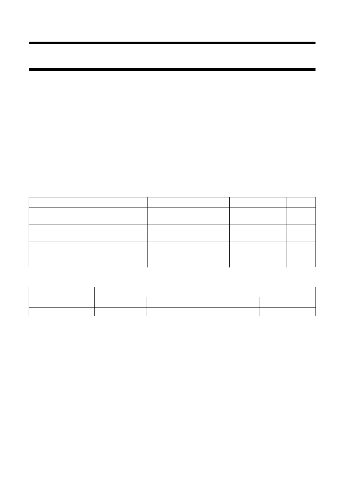
QUICK REFERENCE DATA
SYMBOL PARAMETER CONDITIONS MIN. TYP. MAX. UNIT
V
CC
I
CC
G
v
supply voltage 5.0 8.5 18 V
supply current VCC = 8.5 − 11 14 mA
voltage gain −0.5 0 +0.5 dB
SVRR supply voltage ripple rejection 55 60 − dB
V
no
| input impedance 100 240 − kΩ
|Z
i
CMRR common-mode rejection ratio R
noise output voltage − 3.7 5.0 µV
= 0 Ω−80 − dB
s
GENERAL DESCRIPTION
The TDA8577 is a two channel differential amplifier with
0 dB gain and low distortion. The device has been
primarily developed for car radio applications where long
connections between signal sources and amplifiers (or
boosters) are necessary and where ground noise has to be
eliminated. The device is intended to be used to receive
line inputs in audio applications that require a high level of
common-mode rejection. The device is contained in a
9-pin single in-line package.
ORDERING INFORMATION
EXTENDED TYPE
NUMBER
TDA8577 9 SIL9 plastic SOT142
PACKAGE
PINS PIN POSITION MATERIAL CODE
September 1995 2
Page 3
Philips Semiconductors Preliminary specification
Dual common-mode rejection differential
line receiver
BLOCK DIAGRAM
V
CC
TDA8577
GND
9
8
OUTL
V
CC
5
SVRR
7
OUTR
6
MBD226
INL
INL
INR
INR
1
2
3
4
TDA8577
FUNCTIONAL DESCRIPTION
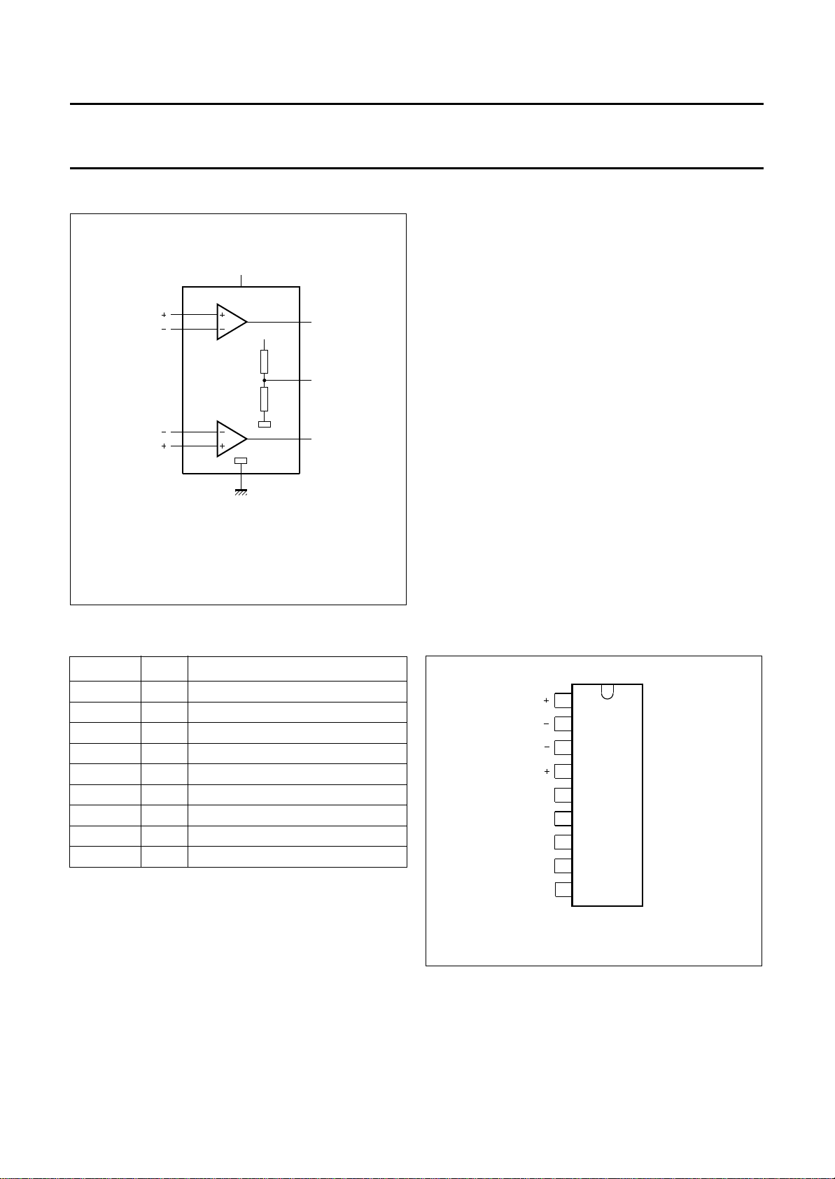
The TDA8577 contains two identical differential amplifiers
with a voltage gain of 0 dB. The device is intended to
receive line input signals for audio applications. The
TDA8577 has a very high level of common-mode rejection
and thus eliminates ground noise. The common-mode
rejection remains constant up to high frequencies (the
amplifier gain is fixed at 0 dB). The inputs have a high input
impedance. The output stage is a class AB stage with a
low output impedance. For a large common-mode
rejection, also at low frequencies, an electrolytic capacitor
connected to the negative input is advised. Because the
input impedance is relatively high, this results in a large
settling time of the DC input voltage. Therefore a
quick-charge circuit is included to charge the input
capacitor within 0.2 seconds.
All input and output pins are protected against high
electrostatic discharge conditions (4000 V, 150 pF, 150 Ω).
Fig.1 Block diagram.
PINNING
SYMBOL PIN DESCRIPTION
INL+ 1 positive input left
INL− 2 negative input left
INR− 3 negative input right
INR+ 4 positive input right
SVRR 5 half supply voltage
GND 6 ground
OUTR 7 output right
OUTL 8 output left
V
CC
9 supply voltage
INL
1
INL
2
INR
3
4
INR
5
SVRR
GND
OUTR
OUTL
V
CC
TDA8577
6
7
8
9
MBD227
Fig.2 Pin configuration.
September 1995 3
Page 4
Philips Semiconductors Preliminary specification
Dual common-mode rejection differential
TDA8577
line receiver
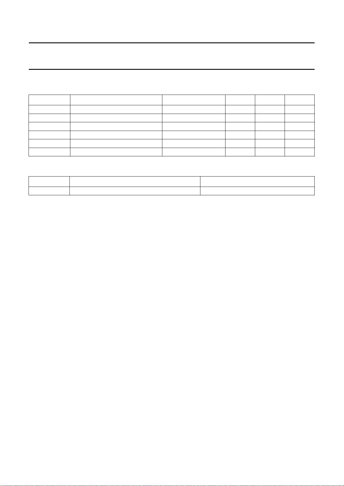
LIMITING VALUES
In accordance with the Absolute Maximum Rating System (IEC 134).
SYMBOL PARAMETER CONDITIONS MIN. MAX. UNIT
V
CC
I
ORM
V
sc
T
stg
T
amb
T
j
THERMAL RESISTANCE
SYMBOL PARAMETER THERMAL RESISTANCE
R
th j-a
supply voltage operating − 18 V
repetitive peak output current − 40 mA
AC and DC short-circuit safe voltage − 18 V
storage temperature −55 +150 °C
operating ambient temperature −40 +85 °C
maximum junction temperature − +150 °C
from junction to ambient in free air 80 K/W
September 1995 4
Page 5
Philips Semiconductors Preliminary specification
Dual common-mode rejection differential
TDA8577
line receiver
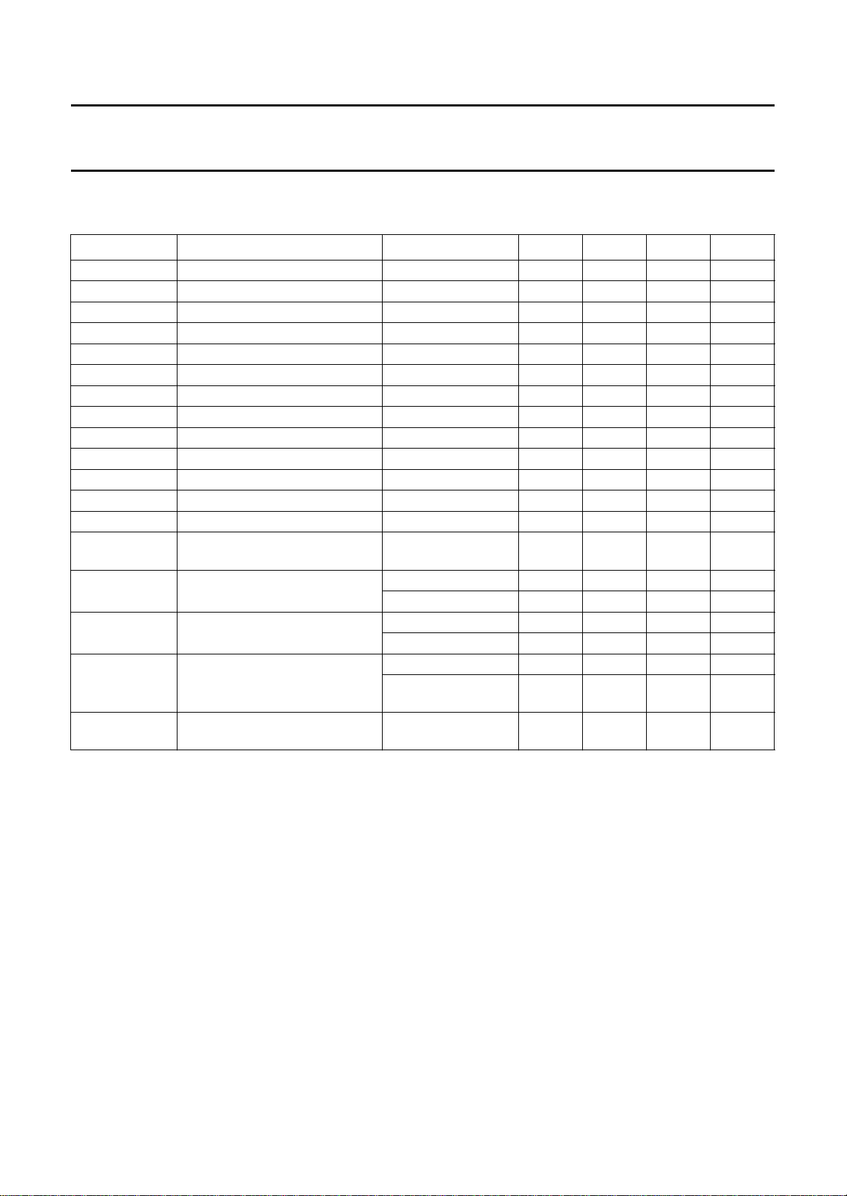
CHARACTERISTICS
V
= 8.5 V; T
CC
SYMBOL PARAMETER CONDITIONS MIN. TYP. MAX. UNIT
V
CC
I
CC
V
O
t
set
G
v
α
cs
| channel unbalance −−0.5 dB
|∆G
v
f
L
f
H
| input impedance 100 240 − kΩ
|Z
i
| output impedance −−10 Ω
|Z
o
V
i(max)
V
no
V
CM(rms)
CMRR common-mode rejection ratio R
SVRR supply voltage ripple rejection note 5 55 65 − dB
THD total harmonic distortion V
THD
max
= 25 °C; f = 1 kHz; measured in test circuit of Fig.3; unless otherwise specified.
amb
supply voltage 5.0 8.5 18 V
supply current − 11 14 mA
DC output voltage note 1 − 4.3 − V
DC input voltage settling time − 0.2 − s
voltage gain −0.5 0 +0.5 dB
channel separation Rs = 5 kΩ 70 80 − dB
low frequency roll-off −1 dB; note 2 20 −−Hz
high frequency roll-off −1 dB 20 −−kHz
maximum input voltage THD = 1% − 2 − V
noise output voltage Rs = 0 Ω; note 3 − 3.7 5.0 µV
common-mode input voltage
−−1V
(RMS value)
= 5 kΩ 66 70 − dB
s
= 0 Ω; note 4 − 80 − dB
R
s
note 6 − 60 − dB
= 1 V; − 0.02 − %
i
= 1 V;
V
i
−−0.1 %
f = 20 Hz to 20 kHz
total harmonic distortion at
Vi = 1 V; RL = 150 Ω− − 1%
maximum output current
Notes
1. The DC output voltage with respect to ground is approximately 0.5V
CC
.
2. The frequency response is externally fixed by the input coupling capacitors.
3. The noise output voltage is measured in a bandwidth of 20 Hz to 20 kHz (unweighted).
4. The common-mode rejection ratio is measured at the output with a voltage source of 1 V (RMS) in accordance with
the test circuit (see Fig.3) while V
INL
and V
are shorted-circuited. Frequencies between 100 Hz and 100 kHz.
INR
5. The ripple rejection is measured at the output, with Rs = 2 kΩ, f = 1 kHz and a ripple amplitude of 2 V (p-p).
6. The ripple rejection is measured at the output, with Rs = 0 to 2 kΩ, f = 100 Hz to 20 kHz and a maximum ripple
amplitude of 2 V (p-p).
September 1995 5
Page 6
Philips Semiconductors Preliminary specification
Dual common-mode rejection differential
line receiver
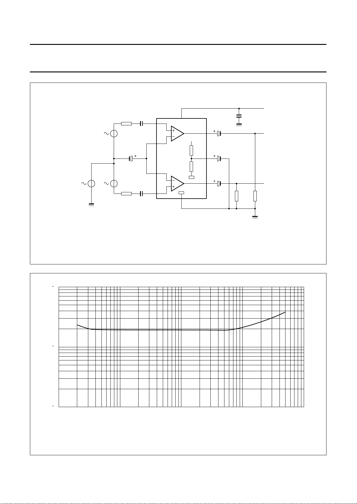
220 nF
R
s
V
INL
5 k
Ω
22 µ
F
V
CM
V
INR
220 nF
R
s
Ω5 k
1
2
3
4
9
TDA8577
SVRR
TDA8577
8.5 V
100 nF
2.2 µ
47 µ
2.2 µ
F
OUTL
F
F
OUTR
R
10 k
MBD229
R
L
L
10 k
Ω
Ω
8
V
CC
5
7
6
10
THD
(%)
10
10
Fig.3 Test circuit.
1
2
3
10
2
10
3
10
4
10
f (Hz)
MBD215
5
10
September 1995 6
Fig.4 Total harmonic distortion as a function of frequency; Vi = 1V (RMS).
Page 7
Philips Semiconductors Preliminary specification
Dual common-mode rejection differential
line receiver
0
CMR
(dB)
20
40
60
80
100
10
(1) Rs = 5 kΩ
(2) Rs = 2 kΩ
(3) Rs = 0 kΩ
2
10
3
10
TDA8577
MBD216
(1)
(2)
(3)
4
10
f (Hz)
5
10
THD
(%)
10
10
10
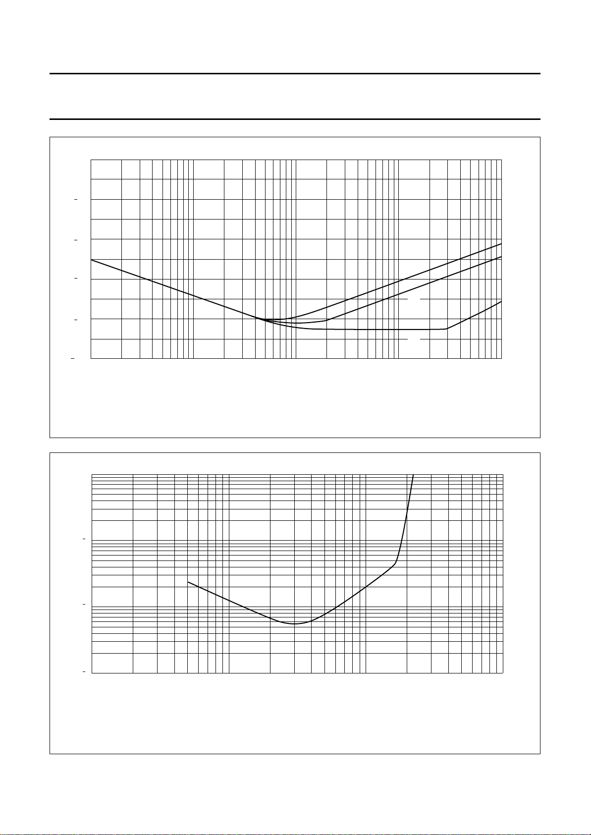
Fig.5 Common-mode rejection ratio as a function of frequency; VCM = 1 V (RMS).
1
1
2
3
2
1010
3
10
V (mV)
i (rms)
MBD213
4
10
September 1995 7
Fig.6 Total harmonic distortion as a function of input voltage; f = 1 kHz.
Page 8
Philips Semiconductors Preliminary specification
Dual common-mode rejection differential
line receiver
40
CMR
(dB)
50
60
70
80
90
100 300 500 700 900
1100
V (mV)
CM (rms)
TDA8577
MBD214
1300
0
CMR
(dB)
20
40
60
80
100
10
(1) C2 = 22 µF
(2) C2 = 47 µF
(3) C2 = 100 µF
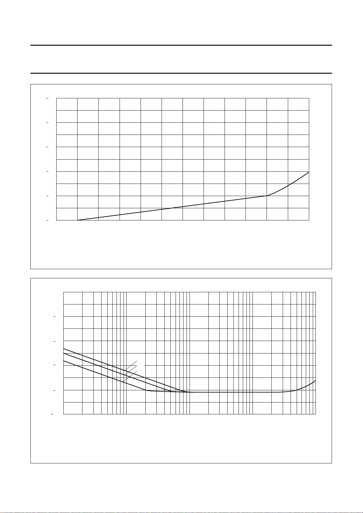
Fig.7 Common-mode rejection ratio as a function of input voltage; f = 1 kHz.
(1)
(2)
(3)
2
10
3
10
4
10
f (Hz)
MBD211
5
10
Fig.8 Common-mode rejection ratio as a function of frequency; VCM = 1 V (RMS).
September 1995 8
Page 9
Philips Semiconductors Preliminary specification
Dual common-mode rejection differential
line receiver
30
SVR
(dB)
40
50
60
70
10
2
10
TDA8577
MBD212
3
10
f (Hz)
4
10
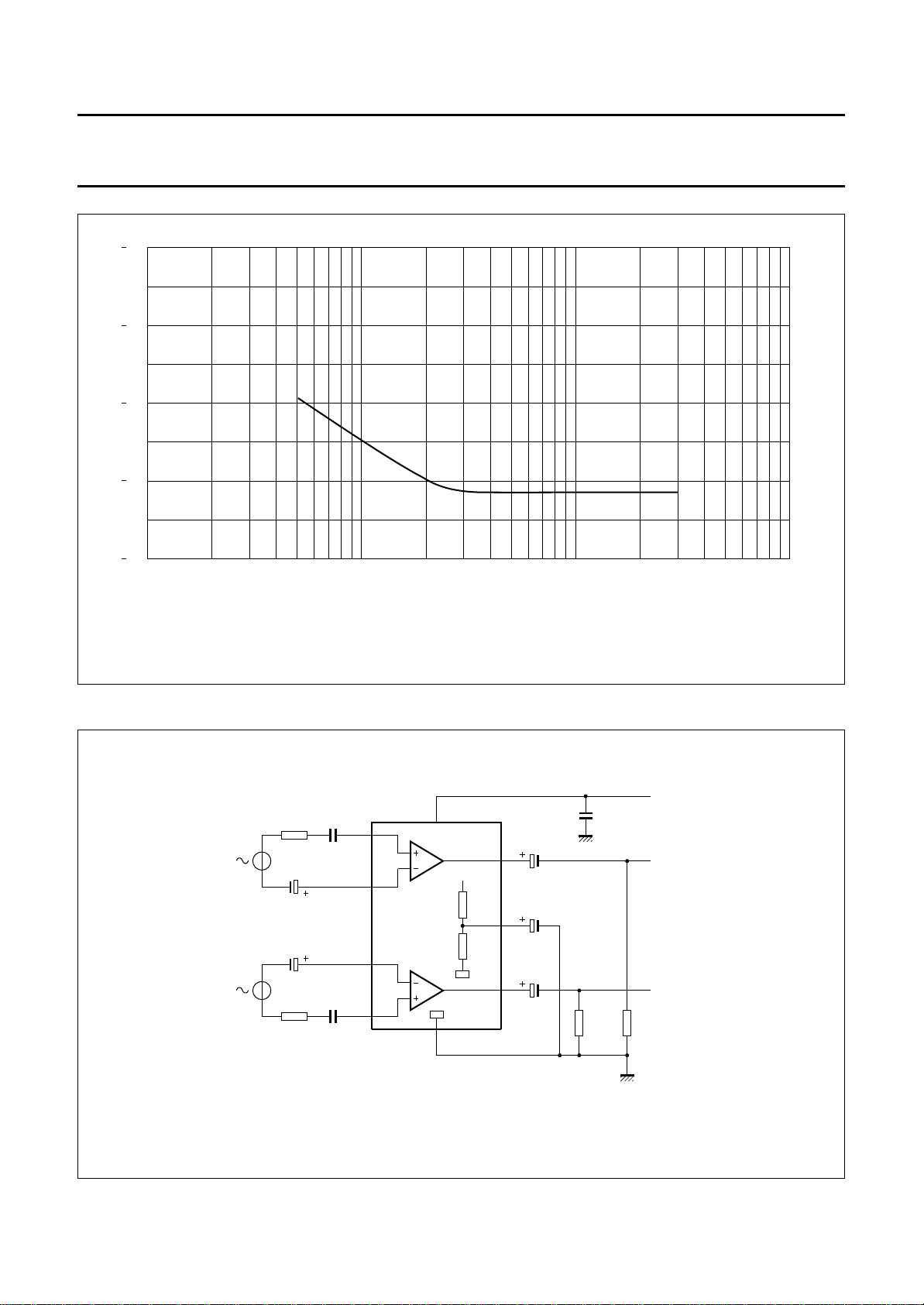
Fig.9 Supply voltage ripple rejection as a function of frequency; V
APPLICATION INFORMATION
V
INL
V
INR
R
s
5 k
10 µF
10 µF
R
s
Ω
Ω5 k
220 nF
220 nF
1
2
TDA8577
3
4
9
SVRR
= 2 V (p-p), Rs = 2 kΩ.
ripple
8.5 V
100 nF
2.2 µ
47 µ
2.2 µ
F
OUTL
F
F
OUTR
R
10 k
MBD228
R
L
L
10 k
Ω
Ω
8
V
CC
5
7
6
September 1995 9
Fig.10 Application circuit with balanced signal source
Page 10
Philips Semiconductors Preliminary specification
Dual common-mode rejection differential
line receiver
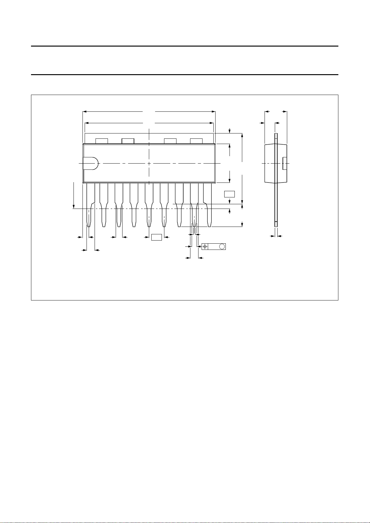
PACKAGE OUTLINE
22.00
21.35
21.4
20.7
5
6789
2.54
(8x)
0.67
0.50
1.40
1.14
seating plane
1.0
0.3
1.40
1.14
1234
1.0
0.7
0.45
0.25
0.25
(9x)
TDA8577
3.85
3.45
1.75
1.55
1.8
1.4
6.48
6.14
12
11
0.76
3.9
3.4
0.47
0.38
M
MBC375
Dimensions in mm.
Fig.11 9-lead single in-line; plastic (SOT142).
SOLDERING
Plastic single in-line packages
B
Y DIP OR WAVE
The maximum permissible temperature of the solder is
260 °C; this temperature must not be in contact with the
joint for more than 5 s. The total contact time of successive
solder waves must not exceed 5 s.
The device may be mounted up to the seating plane, but
the temperature of the plastic body must not exceed the
specified storage maximum. If the printed-circuit board has
been pre-heated, forced cooling may be necessary
immediately after soldering to keep the temperature within
the permissible limit.
R
EPAIRING SOLDERED JOINTS
Apply the soldering iron below the seating plane (or not
more than 2 mm above it). If its temperature is below
300 °C, it must not be in contact for more than 10 s; if
between 300 and 400 °C, for not more than 5 s.
September 1995 10
Page 11

Philips Semiconductors Preliminary specification
Dual common-mode rejection differential
TDA8577
line receiver
DEFINITIONS
Data sheet status
Objective specification This data sheet contains target or goal specifications for product development.
Preliminary specification This data sheet contains preliminary data; supplementary data may be published later.
Product specification This data sheet contains final product specifications.
Limiting values
Limiting values given are in accordance with the Absolute Maximum Rating System (IEC 134). Stress above one or
more of the limiting values may cause permanent damage to the device. These are stress ratings only and operation
of the device at these or at any other conditions above those given in the Characteristics sections of the specification
is not implied. Exposure to limiting values for extended periods may affect device reliability.
Application information
Where application information is given, it is advisory and does not form part of the specification.
LIFE SUPPORT APPLICATIONS
These products are not designed for use in life support appliances, devices, or systems where malfunction of these
products can reasonably be expected to result in personal injury. Philips customers using or selling these products for
use in such applications do so at their own risk and agree to fully indemnify Philips for any damages resulting from such
improper use or sale.
September 1995 11
Page 12

Philips Semiconductors – a worldwide company
Argentina: IEROD, Av. Juramento 1992 - 14.b, (1428)
BUENOS AIRES, Tel. (541)786 7633, Fax. (541)786 9367
Australia: 34 Waterloo Road, NORTH RYDE, NSW 2113,
Tel. (02)805 4455, Fax. (02)805 4466
Austria: Triester Str. 64, A-1101 WIEN, P.O. Box 213,
Tel. (01)60 101-1236, Fax. (01)60 101-1211
Belgium: Postbus 90050, 5600 PB EINDHOVEN, The Netherlands,
Tel. (31)40 783 749, Fax. (31)40 788 399
Brazil: Rua do Rocio 220 - 5
CEP: 04552-903-SÃO PAULO-SP, Brazil.
P.O. Box 7383 (01064-970).
Tel. (011)829-1166, Fax. (011)829-1849
Canada: INTEGRATED CIRCUITS:
Tel. (800)234-7381, Fax. (708)296-8556
DISCRETE SEMICONDUCTORS: 601 Milner Ave,
SCARBOROUGH, ONTARIO, M1B 1M8,
Tel. (0416)292 5161 ext. 2336, Fax. (0416)292 4477
Chile: Av. Santa Maria 0760, SANTIAGO,
Tel. (02)773 816, Fax. (02)777 6730
Colombia: Carrera 21 No. 56-17, BOGOTA, D.E., P.O. Box 77621,
Tel. (571)217 4609, Fax. (01)217 4549
Denmark: Prags Boulevard 80, PB 1919, DK-2300 COPENHAGEN S,
Tel. (032)88 2636, Fax. (031)57 1949
Finland: Sinikalliontie 3, FIN-02630 ESPOO,
Tel. (9)0-50261, Fax. (9)0-520971
France: 4 rue du Port-aux-Vins, BP317,
92156 SURESNES Cedex,
Tel. (01)4099 6161, Fax. (01)4099 6427
Germany: P.O. Box 10 63 23, 20095 HAMBURG ,
Tel. (040)3296-0, Fax. (040)3296 213
Greece: No. 15, 25th March Street, GR 17778 TAVROS,
Tel. (01)4894 339/4894 911, Fax. (01)4814 240
Hong Kong: 15/F Philips Ind. Bldg., 24-28 Kung Yip St.,
KWAI CHUNG, Tel. (0)4245 121, Fax. (0)4806 960
India: PEICO ELECTRONICS & ELECTRICALS Ltd.,
Components Dept., Shivsagar Estate, Block 'A',
Dr. Annie Besant Rd., Worli, BOMBAY 400 018,
Tel. (022)4938 541, Fax. (022)4938 722
Indonesia: Philips House, Jalan H.R. Rasuna Said Kav. 3-4,
P.O. Box 4252, JAKARTA 12950,
Tel. (021)5201 122, Fax. (021)5205 189
Ireland: Newstead, Clonskeagh, DUBLIN 14,
Tel. (01)640 000, Fax. (01)640 200
Italy: Viale F. Testi, 327, 20162 MILANO,
Tel. (02)6752.1, Fax. (02)6752.3350
Japan: Philips Bldg13-37 , Kohnan 2-chome, Minato-ku, KOKIO 108,
Tel. (03)3740 5101, Fax. (03)3740 0570
Korea: (Republic of) Philips House, 260-199 Itaewon-dong,
Yongsan-ku, SEOUL, Tel. (02)794-5011, Fax. (02)798-8022
Malaysia: No. 76 Jalan Universiti, 46200 PETALING JAYA,
SELANGOR, Tel. (03)757 5511, Fax. (03)757 4880
Mexico: Philips Components, 5900 Gateway East, Suite 200,
EL PASO, TX 79905, Tel. 9-5(800)234-7381, Fax. (708)296-8556
Netherlands: Postbus 90050, 5600 PB EINDHOVEN,
Tel. (040)78 37 49, Fax. (040)78 83 99
New Zealand: 2 Wagener Place, C.P.O. Box 1041, AUCKLAND,
Tel. (09)849-4160, Fax. (09)849-7811
Norway: Box 1, Manglerud 0612, OSLO,
Tel. (22)74 8000, Fax. (22)74 8341
th
floor, Suite 51,
Pakistan: Philips Markaz, M.A. Jinnah Rd., KARACHI 3,
Tel. (021)577 039, Fax. (021)569 1832
Philippines: PHILIPS SEMICONDUCTORS PHILIPPINES Inc,
106 Valero St. Salcedo Village, P.O. Box 911, MAKATI,
Metro MANILA, Tel. (02)810 0161, Fax. (02)817 3474
Portugal: Av. Eng. Duarte Pacheco 6, 1009 LISBOA Codex,
Tel. (01)683 121, Fax. (01)658 013
Singapore: Lorong 1, Toa Payoh, SINGAPORE 1231,
Tel. (65)350 2000, Fax. (65)251 6500
South Africa: 195-215 Main Road, Martindale,
P.O. Box 7430,JOHANNESBURG 2000,
Tel. (011)470-5433, Fax. (011)470-5494
Spain: Balmes 22, 08007 BARCELONA,
Tel. (03)301 6312, Fax. (03)301 42 43
Sweden: Kottbygatan 7, Akalla. S-164 85 STOCKHOLM,
Tel. (0)8-632 2000, Fax. (0)8-632 2745
Switzerland: Allmendstrasse 140, CH-8027 ZÜRICH,
Tel. (01)488 2211, Fax. (01)481 7730
Taiwan: 69, Min Sheng East Road, Sec 3, P.O. Box 22978,
TAIPEI 10446, Tel. (2)509 7666, Fax. (2)500 5899
Thailand: PHILIPS ELECTRONICS (THAILAND) Ltd.,
60/14 MOO 11, Bangna - Trad Road Km. 3
Prakanong, BANGKOK 10260,
Tel. (2)399-3280 to 9, (2)398-2083, Fax. (2)398-2080
Turkey: Talatpasa Cad. No. 5, 80640 LEVENT/ISTANBUL,
Tel. (0212)279 2770, Fax. (0212)269 3094
United Kingdom: Philips Semiconductors Limited, P.O. Box 65,
Philips House, Torrington Place, LONDON, WC1E 7HD,
Tel. (071)436 41 44, Fax. (071)323 03 42
United States:INTEGRATED CIRCUITS:
811 East Arques Avenue, SUNNYVALE, CA 94088-3409,
Tel. (800)234-7381, Fax. (708)296-8556
DISCRETE SEMICONDUCTORS: 2001 West Blue Heron Blvd.,
P.O. Box 10330, RIVIERA BEACH, FLORIDA 33404,
Tel. (800)447-3762 and (407)881-3200, Fax. (407)881-3300
Uruguay: Coronel Mora 433, MONTEVIDEO,
Tel. (02)70-4044, Fax. (02)92 0601
For all other countries apply to: Philips Semiconductors,
International Marketing and Sales, Building BAF-1,
P.O. Box 218, 5600 MD, EINDHOVEN, The Netherlands,
Telex 35000 phtcnl, Fax. +31-40-724825
SCD27 © Philips Electronics N.V. 1993
All rights are reserved. Reproduction in whole or in part is prohibited without the
prior written consent of the copyright owner.
The information presented in this document does not form part of any quotation
or contract, is believed to be accurate and reliable and may be changed without
notice. No liability will be accepted by the publisher for any consequence of its
use. Publication thereof does not convey nor imply any license under patent- or
other industrial or intellectual property rights.
Printed in The Netherlands 9397 726 70011
Philips Semiconductors
 Loading...