

Page 1

INTEGRATED CIRCUITS
DATA SH EET
TDA8505
SECAM encoder
Preliminary specification
Supersedes data of May 1993
File under Integrated Circuits, IC02
Philips Semiconductors
July 1994
Page 2

Philips Semiconductors Preliminary specification
SECAM encoder TDA8505
FEATURES
• Two input stages, R, G, B and Y, −(R−Y), −(B−Y) with
multiplexing.
• Chrominance processing, highly integrated, includes
vertical identification, low frequency pre-emphasis and
high frequency pre-emphasis (anti-Cloche) and
bandpass filter.
• Fully controlled FM modulator which produces a signal
in accordance with the SECAM standard without
adjustments.
• Two reference oscillators, one for D'R f
and one for D'B f0 (4.250 MHz). These oscillators are
tuned by PLL loop with the frequency of the line sync as
reference. Crystal tuning, or tuning by external
reference source, of the reference oscillators is
possible.
• Output stages, CVBS and separated Y + SYNC and
CHROMA. For CVBS output, signal amplitude 2 V (p−p)
nominal, thus only an external emitter follower is
required for 75 Ω driving.
• Sync separator circuit and pulse shaper, to generate the
required pulses for the processing, line, frame, FH/2 and
chrominance blanking.
(4.40625 MHz)
0
GENERAL DESCRIPTION
The TDA8505 is a highly integrated SECAM encoding IC
that is designed for use in all applications that require
transformation of R, G and B signals or Y, U and V signals
to a standard SECAM signal.
The specification of the input signals is fully compatible
with those of the TDA8501 PAL/NTSC encoder.
• A 3-level sandcastle pulse is generated for PAL/NTSC
to SECAM transcoding.
• FH/2 input for locking with another decoder.
• Colour killing on the internal colour difference signals.
• Internal bandgap reference.
ORDERING INFORMATION
TYPE NUMBER
PINS PIN POSITION MATERIAL CODE
TDA8505 32 SDIP32 plastic SOT232-1
PACKAGE
July 1994 2
Page 3
Philips Semiconductors Preliminary specification
SECAM encoder TDA8505
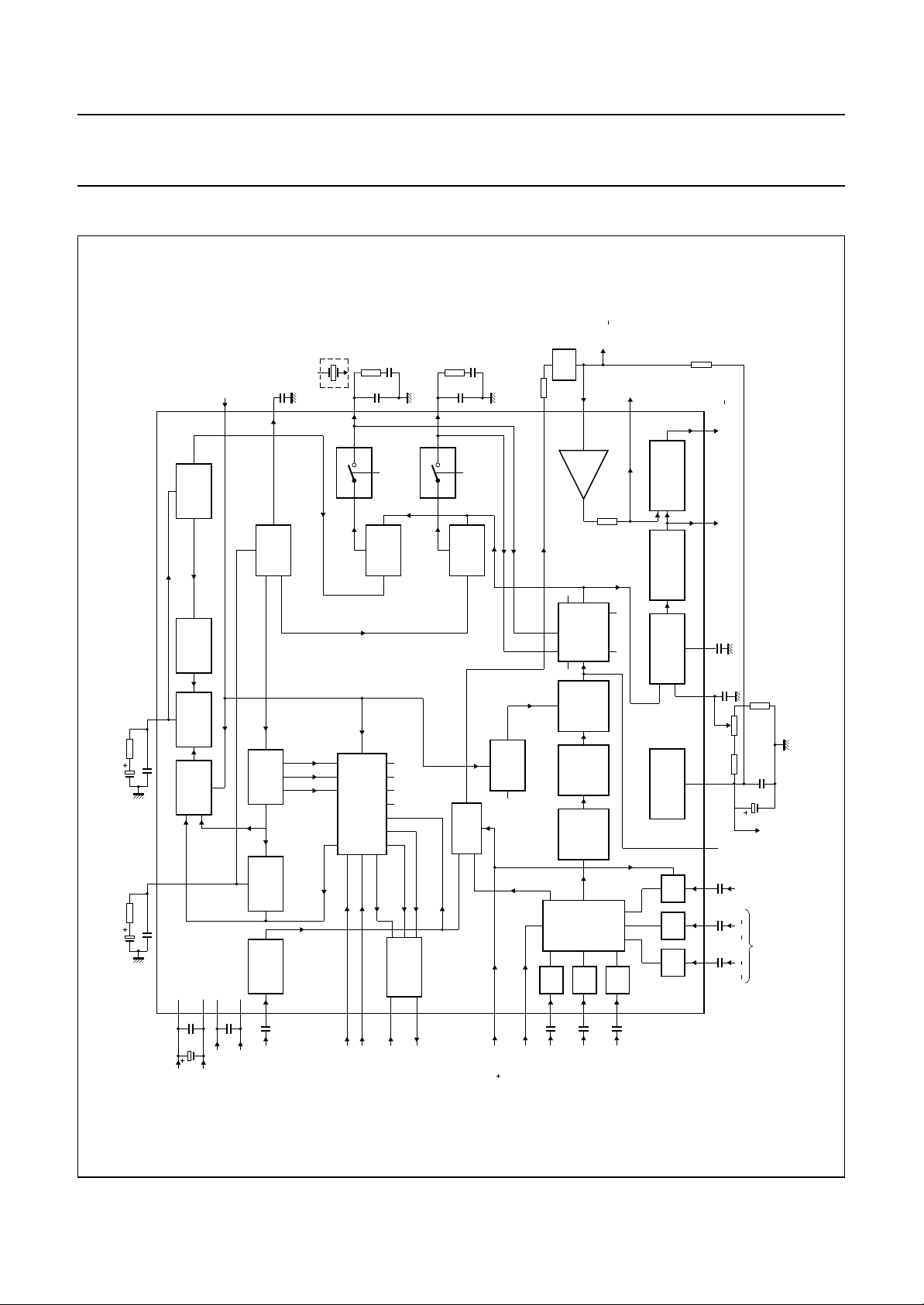
BLOCK DIAGRAM
Y+SYNC
1 V (p p)
470 nF
100 Ω
nF
6.8
15
Y+SYNC output
LPFDB output
2 V (p-p)
25
LINE
DELAY
ns
650
23
input
Y+SYNC
notch
22
output
21
MLA951 - 3
CVBS 2 V (p p)
output
XTAL/PLL
VIDENT
input
26
1 µF
3.9 kΩ
270 pF
output
VCO4.25
27
1 nF
13
LPFDR output
4.7 µF
4.7 µF
1.2 kΩ
2.2 kΩ
100 nF
output
LPF 4.4
22 nF
output
LPF4.25
24
31
8
VCO
4.406 MHz
282
DIVIDER
PHASE
DETECTOR
SWITCH
32
10
30
VCO
4.25 MHz
272
DIVIDER
PHASE
DETECTOR
SYNC
SEPARATOR
29
28
PHASE
PULSE
GENERATOR
4
DETECTOR
SANDCASTLE
19external power
20
PHASE
DETECTOR
TDA8505
ADDER
12
FRAME
IDENTI-
FICATION
7
2
CL/BL
BUFFER
FM
PHASE
MODULATOR
GAIN
ADDER
LIMITER
CLAMP
FILTER
LF PRE-
EMPHASIS
LOW-PASS
MATRIX
SWITCH
SEQUENCE
CL/BL
9
2 kΩ
SWITCH
CL/BL
11
ADDER
18
BLANKING
CHROMINANCE
16
FILTER
CLOCHE BANDPASS
ref
V
CL/BL CL/BL CL/BL
14
FADJ
17
V
6
5
3
1
output
chrominance
nF
220
FLT output
22
nF
kΩ
4.7
1.8 kΩ
ref
TEST
47
nF
47
nF
47
nF
22 kΩ
22 nF
47
µF
reference
input
luminance
(B Y)
inputs
(R Y)
colour difference
output
voltage
handbook, full pagewidth
Fig.1 Block diagram.
V
DDD
100 nF
SSD
V
22 nF
sync
input
composite
input
FH/2 input
colour killing
ext
output
sandcastle
supply (V )
V
DDA
22
nF
47 µF
V
SSA
July 1994 3
multiplexer
control input
(Y/Y SYNC)
47
RED
input
control input
nF
GREEN
input
47
47
nF
nF
input
BLUE
Page 4

Philips Semiconductors Preliminary specification
SECAM encoder TDA8505
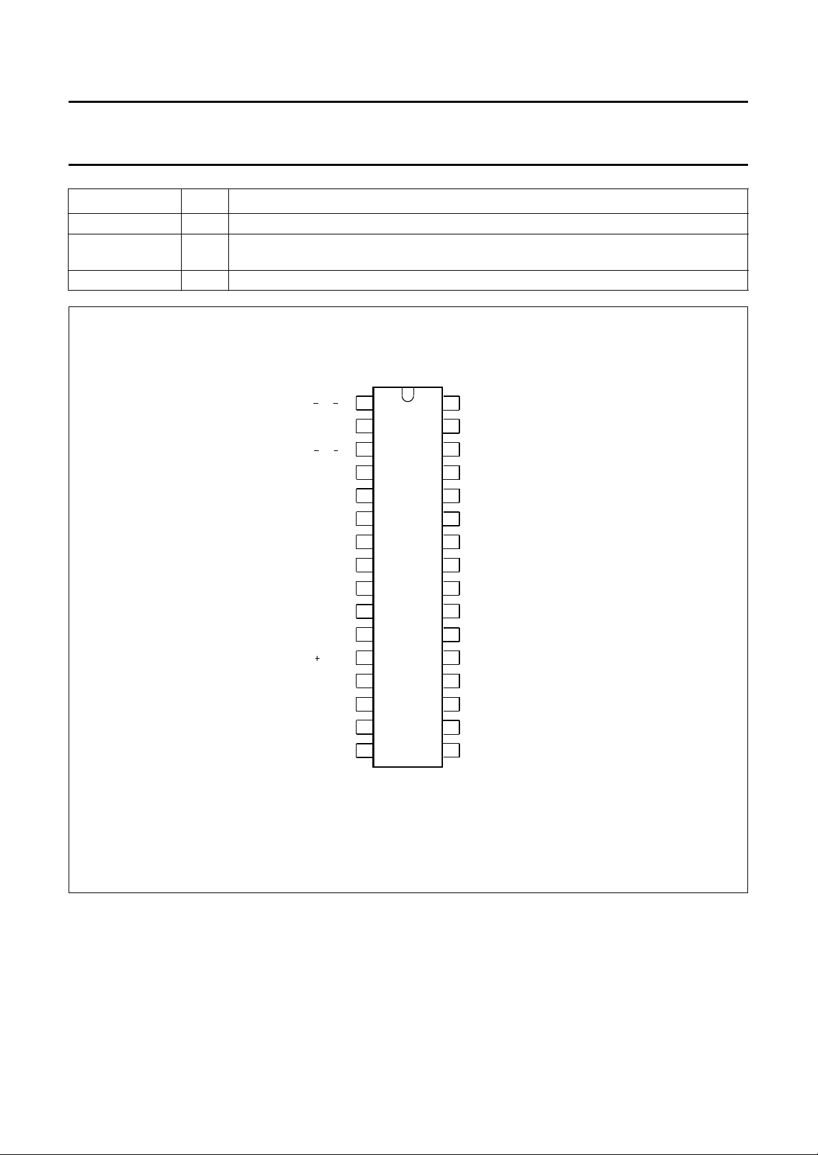
PINNING
D'R and D'B are the colour difference signals at the output of the multiplexer circuit; D'R = −1.9(R−Y) and
D'B = +1.5(B−Y), for an EBU bar of 75% the amplitudes are equal.
SYMBOL PIN DESCRIPTION
−(R−Y) 1 colour difference input signal, for EBU bar of 75% 1.05 V (peak-to-peak value)
MCONTR 2 multiplexer control; input HIGH = RGB, input LOW = −(R−Y), −(B−Y) and Y
−(B−Y) 3 colour difference input signal, for EBU bar of 75% 1.33 V (peak-to-peak value)
FH/2 4 line pulse input divided-by-2 for synchronizing two or more encoders; when not used this
pin is connected to ground
Y 5 luminance input signal 1 V nominal without sync
TEST 6 test pin; must be connected to V
R 7 RED input signal for EBU bar of 75% 0.7 V (peak-to-peak value)
V
DDA
8 analog supply voltage for encoder part; 5 V nominal
G 9 GREEN input signal for EBU bar of 75% 0.7 V (peak-to-peak value)
V
SSA
10 analog ground
B 11 BLUE input signal for EBU bar of 75% 0.7 V (peak-to-peak value)
Y/Y+SYNC 12 when this control input is LOW, Y without sync is connected to pin 5, input blanking at
pin 5 is active; when input is HIGH, Y+SYNC is connected to pin 5, input blanking at pin 5
is not active
LPFDR 13 modulator control loop filter output; black level of D'R = 4.40625 MHz
FADJ 14 adjustment pin for 4.286 MHz of HF pre-emphasis filter
LPFDB 15 modulator control loop filter output; black level of D'B = 4.250 MHz
FLT 16 filter tuning loop capacitor output
V
ref
17 2.5 V internal reference voltage output
CHROMA 18 chrominance output, amplitude corresponds with Y+SYNC at the output of the delay line
V
ext
19 external power supply for sandcastle generation; when not used this pin is connected to
ground
SAND 20 3-level sandcastle output pulse
CVBS 21 composite SECAM output 2 V (peak-to-peak value) nominal
NOTCH 22 Y+SYNC output after an internal resistor of 2 kΩ; a notch filter can be connected
Y+SYNC IN 23 Y+SYNC input, connected to the output of the delay line
LPF4.4 24 loop filter output for 4.40625 MHz reference oscillator
Y+SYNC OUT 25 Y+SYNC output, 2 V (peak-to-peak value) nominal, connected to the input of the
delay line
XTAL/PLL
VIDENT
26 control pin; input HIGH = crystal tuning, input LOW = PLL tuning, both without vertical
identification, 2.5 V = PLL tuning with vertical identification
VCO4.25 27 when used for PLL tuning a capacitor is connected; when used for crystal tuning a crystal
has to be connected (in series with a capacitor)
COLKIL 28 colour killing; input HIGH = active, internal colour difference signals are blanked
CS 29 composite sync input, 0.3 V (peak-to-peak value) nominal
(pin 8), or left open-circuit
CC
July 1994 4
Page 5
Philips Semiconductors Preliminary specification
SECAM encoder TDA8505
SYMBOL PIN DESCRIPTION
V
SSD
LPF4.25 31 loop filter output for 4.25 MHz reference oscillator; connected to pin 17 (V
V
DDD
30 digital ground
external tuning by crystal or signal source
32 supply voltage for the digital part
) when
ref
handbook, halfpage
MCONTR
Y/Y SYNC
(R Y)
(B Y)
FH/2
TEST
V
DDA
V
SSA
LPFDR
FADJ
LPFDB
FLT
1
2
3
4
Y
5
6
R
7
8
9
10
11
12
13
14
15
16
TDA8505
MLA952 - 3
G
B
V
DDD
32
31
LPF4.25
V
30
SSD
CS
29
COLKIL
28
VCO4.25
27
XTAL/PLL
26
VIDENT
Y+SYNC OUT
25
LPF4.4
24
23
Y+SYNC IN
NOTCH
22
21
CVBS
SAND
20
V
19
ext
18
CHROMA
V
17
ref
Fig.2 Pin configuration.
July 1994 5
Page 6
Philips Semiconductors Preliminary specification
SECAM encoder TDA8505
FUNCTIONAL DESCRIPTION
The following three important circuits are integrated:
• Encoder circuit
• Modulator control circuit
• Sync separator and pulse shaper.
Encoder circuit
I
NPUT STAGE
R, G and B inputs are connected to the matrix via a
clamping and a blanking circuit.
For an EBU colour bar of 75% the amplitude of the signal
must be 0.7 V (peak-to-peak value). The outputs of the
matrix are Y, D'R and D'B.
The second part of the input stage contains inputs for
colour difference signals and a luminance signal. The
condition for 75% colour bar is
−(R−Y) = 1.05 V (peak-to-peak value) at pin 1,
−(B−Y) = 1.33 V (peak-to-peak value) at pin 3 and
Y = 1 V (peak-to-peak value) without sync at pin 5. After
clamping and blanking the amplitude and polarity are
corrected such that the signals are equal to the signals of
the matrix output. Signals are connected to a switch. Fast
switching between the two input parts is possible by the
multiplexer control pin (pin 2).
The Y output signal of the multiplexer is added to the sync
pulse of the sync separator.
The Y input (pin 5) is different to the other 5 inputs. The
timing of the internal clamping is after the sync period and
there is no vertical blanking.
The input blanking of Y can be switched off by a HIGH at
pin 12, and the internal sync separator signal is not added
to the Y signal. In this way the Y+SYNC is allowed at pin 5
and after clamping internally connected directly to pin 25.
The colour difference signals are switched sequentially by
H/2 and fed to the low frequency pre-emphasis circuit.
The colour-killing input signal at pin 28 can be used for
completely blanking the internal colour difference signals
at the input of the low frequency pre-emphasis filter.
LOW FREQUENCY PRE-EMPHASIS
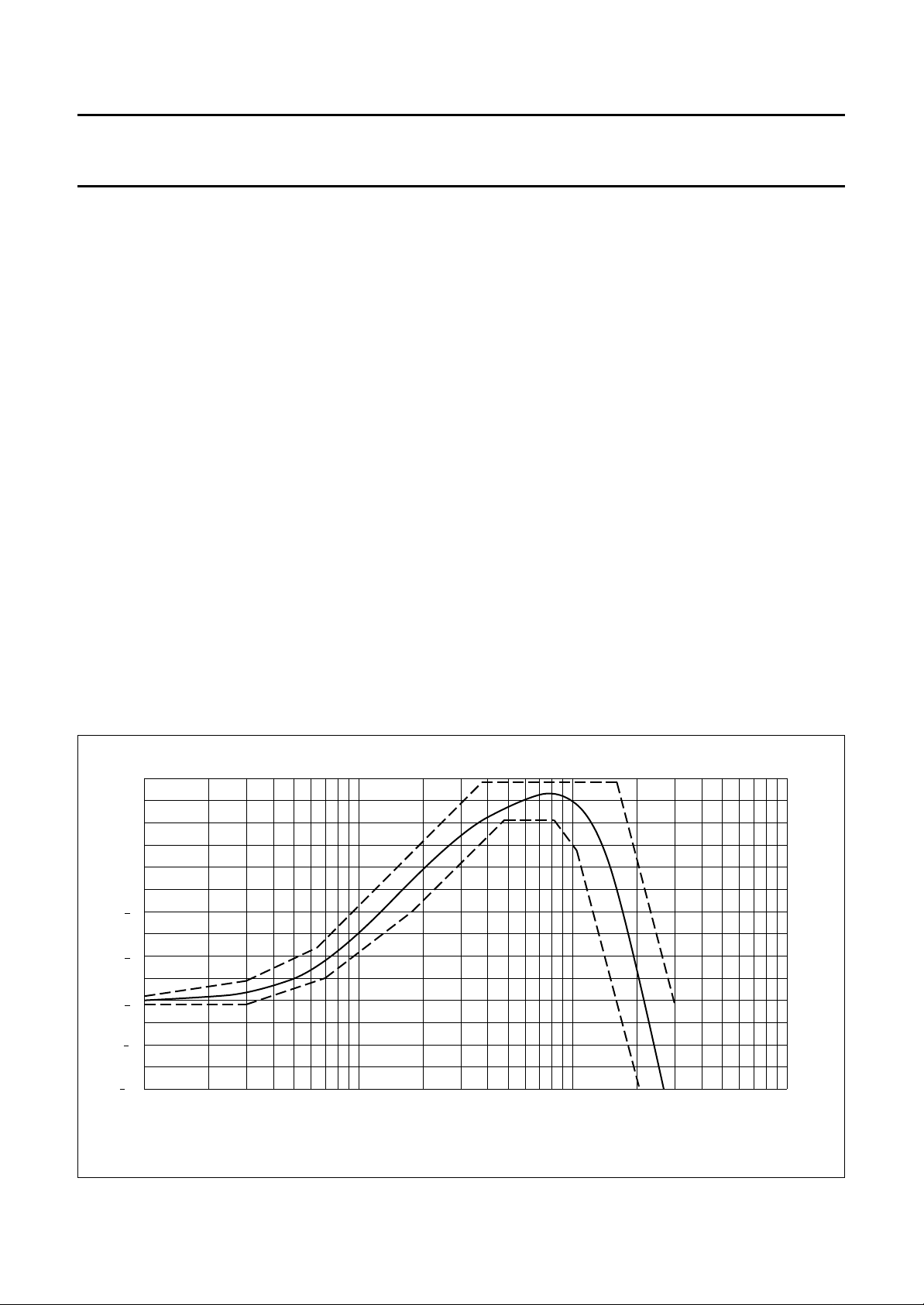
This filter is fully integrated, Fig.3 illustrates the nominal
response.
The transfer is guaranteed within the illustrated area for
the whole ambient temperature range by a compensation
circuit.
H
(dB)
4
2
0
2
4
6
8
10
4
10
5
10
handbook, full pagewidth
Fig.3 Nominal response for the low frequency pre-emphasis filter.
July 1994 6
MLA953 - 1
6
10
f (Hz)
7
10
Page 7

Philips Semiconductors Preliminary specification
SECAM encoder TDA8505
VERTICAL IDENTIFICATION
After the low frequency pre-emphasis the signal is
clamped and, if desired the vertical identification sawtooth
waveform can be added. The generation of the vertical
identification is switched on/off by the logic level input at
pin 26.
Figure 4 shows the sawtooth waveform at the input of the
FM modulator with the corresponding frequency values
after modulation.
Vertical identification is only possible if PLL tuning is
selected.
AIN + LIMITER
G
The gain of this amplifier is sequentially switched, so that
the amplitude of D'R is 280/230 times the amplitude of D'B
(based on an EBU colour bar). The signal is limited at a
lower and upper level to ensure that the FM modulator
frequencies are always between 3.9 MHz and 4.756 MHz.
A DC offset between D'R and D'B is added which
corresponds with the limiter levels.
MODULATOR
FM
The signal of the gain + limiter stage is fed to the FM
modulator.
level of D'R. The modulator control also sets the DC level
at pin 15 to adjust the FM frequency to 4.250 MHz at the
black level of D'B.
At the start of every line the FM modulator is stopped and
is started again by a short duration pulse of the pulse
shaper. These stop/start pulses are operating such that
after two lines starting in the same phase, the start phase
of the third line is shifted 180 degrees. This sequence is
inverted during each vertical blanking.
The FM signal is fed to the internal HF pre-emphasis filter.
HF PRE-EMPHASIS AND BANDPASS FILTER
An HF pre-emphasis filter combined with a bandpass filter
is integrated.
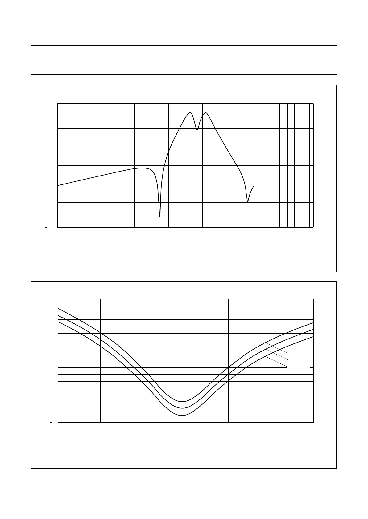
Figures 5 and 6 illustrate the frequency response. Two
resistors in series with a potentiometer at pin 14 adjusts
the frequency to 4.286 MHz with a tolerance of ±20 kHz.
A tuning circuit integrated with an external capacitor
connected to pin 16 guarantees a stable frequency
response for the whole temperature range.
The output of the bandpass filter is connected directly to
the chrominance blanking circuit.
The modulator control adjusts the DC level at pin 13 to set
the frequency of the FM signal to 4.406 MHz at the black
handbook, full pagewidth
15 sµ
5 sµ
D'R
18 sµ
Fig.4 Vertical identification sawtooth waveform input.
6 sµ
frequency
after
64 µs64 µs
D'B
MLA954
modulation
4.756 MHz
35 kHz
4.406 MHz
4.250 MHz
3.90 MHz
35 kHz
July 1994 7
Page 8
Philips Semiconductors Preliminary specification
SECAM encoder TDA8505
H
(dB)
100
0
20
40
60
80
5
10
6
10
7
10
f (Hz)
handbook, full pagewidth
Fig.5 Frequency response of the HF pre-emphasis and bandpass filter; H as a function of frequency (1).
MLA955 - 1
8
10
16
handbook, full pagewidth
H
(dB)
14
12
10
8
6
4
2
0
2
3.7 4.1 4.5
3.9 4.3 4.7
Fig.6 Frequency response of the HF pre-emphasis and bandpass filter; H as a function of frequency (2).
MLA956 - 1
upper limit
nominal
lower limit
f (MHz)
4.9
July 1994 8
Page 9
Philips Semiconductors Preliminary specification
SECAM encoder TDA8505
CHROMINANCE BLANKING
The chrominance signal is blanked by the internally
generated chrominance blanking pulse. The output of this
blanking stage is connected to the chrominance and
CVBS output circuits.
Y+SYNC, CVBS,
AND CHROMA OUTPUTS
The Y output signal of the matrix is added to the composite
sync signal of the sync separator. The output of this adder
at pin 25 is connected to the input of an external delay line
which is necessary for correct timing of the Y+SYNC signal
corresponding with the chrominance signal. The signal
amplitude at pin 25 is 2 V (peak-to-peak value) nominal,
so at the output of the delay line Y+SYNC is
1 V (peak-to-peak value).
The delay line has to be DC-coupled between
pins 25 and 23 to ensure the required DC level at
pin 23. The output resistor of the delay line has to be
connected to pin 17 where (V
= 2.5 V).
ref
The output of the delay line is connected to pin 23 which is
the input of a buffer operational amplifier. The output of the
buffer operational amplifier is connected to pin 22 and to
the CVBS adder stage via an internal resistor of 2 kΩ. An
external notch filter can be connected to pin 22. The CVBS
signal amplitude output at pin 21 is 2 V (peak-to-peak
value) nominal. An external emitter follower is used to
provide a 75 Ω output load.
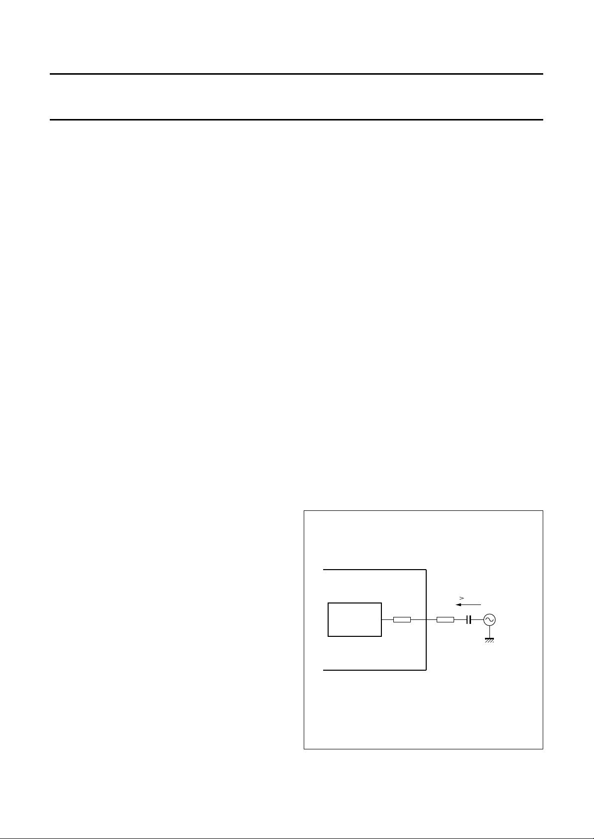
The outputs of the 272 divider are also used for pulse
shaping.
Within the vertical blanking period, another two Phase
Locked Loops (PLLs) synchronizes the FM modulator
during two lines with the 4.406 MHz reference VCO and
during the following 2 lines with the 4.250 MHz reference
VCO. The loop filters are connected to pins 13 and 15
respectively.
It is necessary to use low-leakage capacitors for these
loop filters.
T
UNING BY CRYSTAL OR EXTERNAL SIGNAL SOURCE
When the frequency of the sync pulse at pin 29 is not
stable or is incorrect it is possible to tune the FM modulator
using an external 4.250 MHz crystal connected to pin 27.
The 4.25 MHz loop at pin 31 has to be connected to pin 17
(V
). A stable line frequency reference is generated by
ref
the 272 divider circuit which is used for the 4.406 MHz
reference loop.
An external signal source, instead of a crystal, can be
connected at pin 27 via a capacitor in series with a resistor.
The minimum AC current of 50 µA is determined by the
resistor values (R
int+Rext
) and the output voltage of the
signal source (see Fig.7).
When crystal tuning is used no vertical identification
is possible.
The amplitude of the chrominance output signal which is
connected to pin 18 corresponds with the Y+SYNC signal
at the output of the delay line.
Modulator control circuit
The modulator control circuit has two tuning modes which
are controlled by the input at pin 26:
• Tuning by line frequency
• Tuning by crystal or external signal source.
UNING BY LINE FREQUENCY
T
Two reference voltage controlled oscillators (VCOs) are
integrated, the 4.4 MHz VCO with an internal capacitor
and the 4.25 MHz VCO with an external capacitor at
pin 27.
A PLL loop with divider circuits directly couples the
frequencies of the two VCOs with the line frequency of the
sync separator sync signal.
The loop filter for the 4.40625 MHz reference is at pin 24
and the loop filter for the 4.250 MHz reference is at pin 31.
July 1994 9
Crystal tuning is recommended for VTR signals.
handbook, halfpage
TDA8505
OSCILLATOR
R
int
800Ω
27
R
ext
MSA732 - 1
µ
I 50 A
1 nF
Fig.7 Tuning circuit for external signal source.
signal
source
V (p-p)
Page 10
Philips Semiconductors Preliminary specification
SECAM encoder TDA8505
Sync separator and pulse shaper
The composite sync input at pin 29 together with the
outputs of the 272 divider of the 4.250 MHz reference loop
are the sources for all pulses necessary for the processing.
The pulses are used for:
• Clamping
• Video blanking
• FH/2
• Chrominance blanking
• Stop/start of modulator
• Vertical identification
• Timing for the modulator control
• Sandcastle pulse shaping at pin 20.
External FH/2 at pin 4 is only necessary when two or more
SECAM encoders have to be locked in the same phase.
The phase of the internal FH/2 can be locked with an
external FH/2 connected at pin 4. A reset of the internal
FH/2 is possible by forcing pin 4 to a HIGH level. This
HIGH level corresponds with D'R. Pin 4 is connected to
ground when not used.
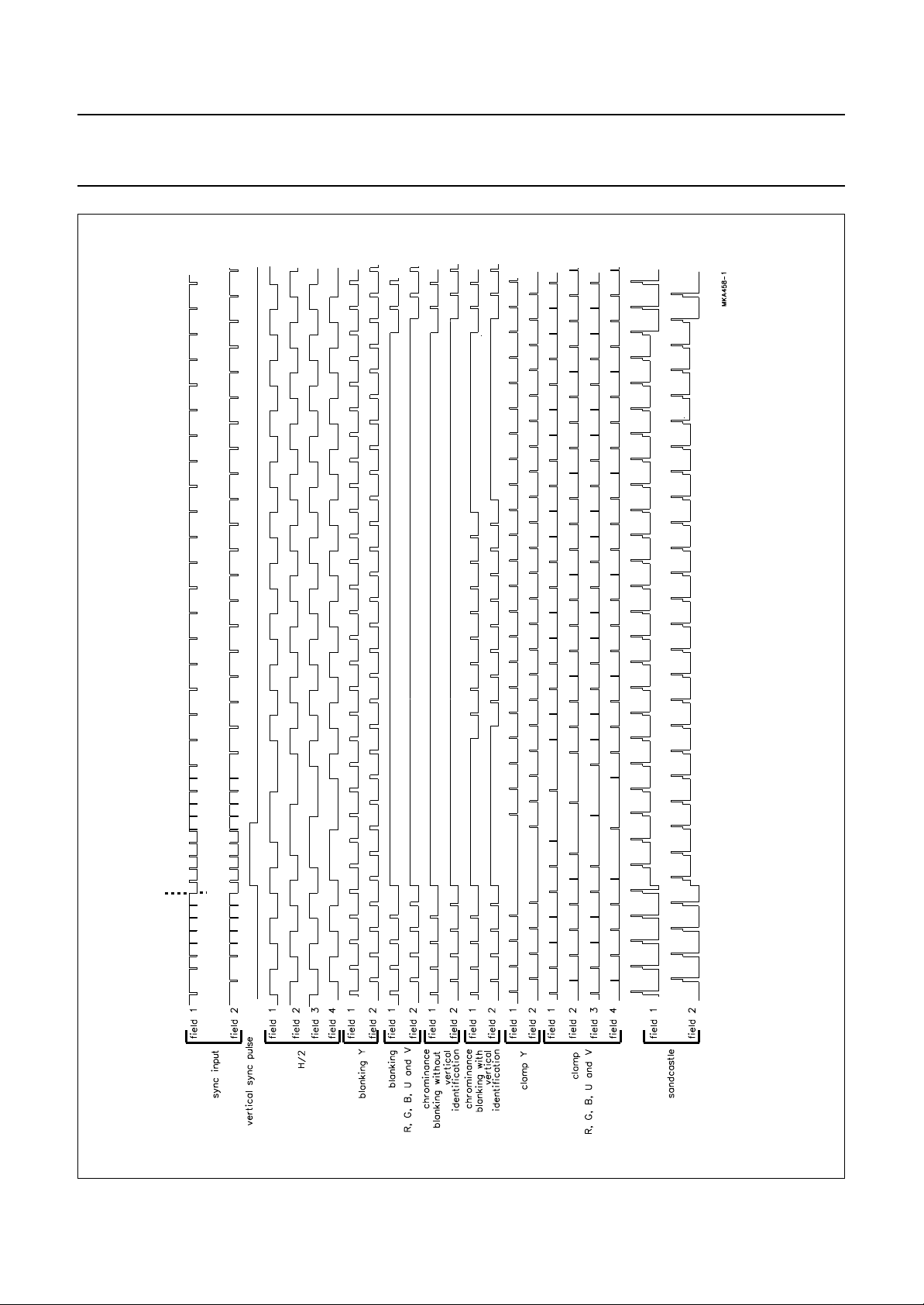
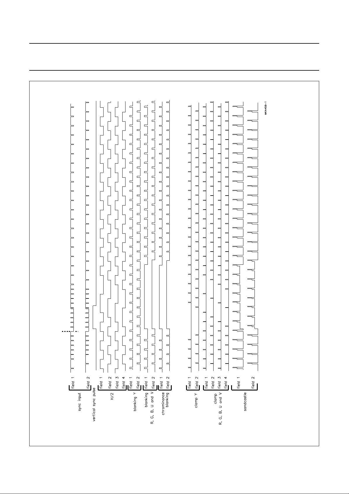
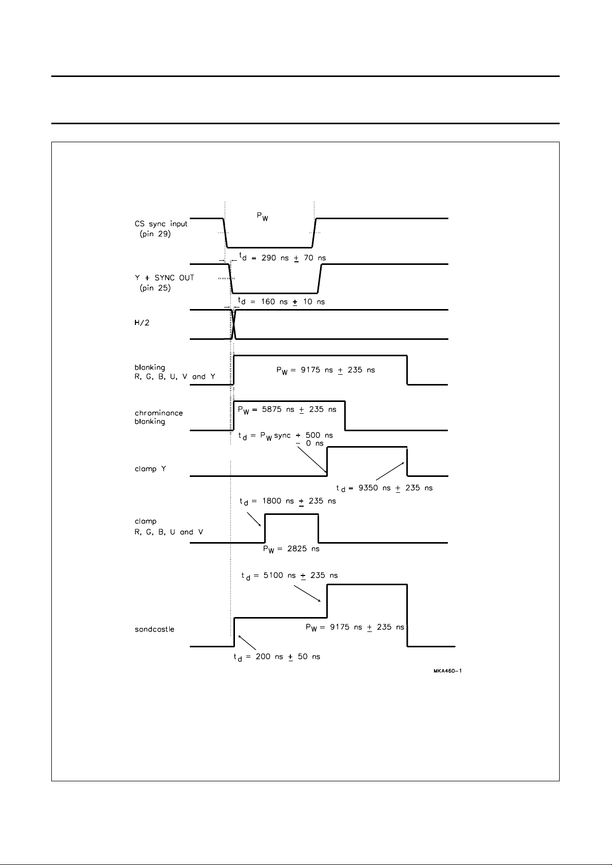
Figures 9 and 10 show the generated pulses during
vertical blanking for PLL tuning or crystal tuning
respectively. Figure 11 shows the pulses during line
blanking.
Transcoding application
A sandcastle pulse is necessary for the PAL/NTSC
demodulator (i.e. TDA4510) for transcoding PAL or NTSC
to SECAM.
Most of the demodulator ICs use a sandcastle pulse with
an amplitude of 12 V or 8 V. A 12 V or 8 V sandcastle is
not possible with the TDA8505 because of the 5 V power
supply.
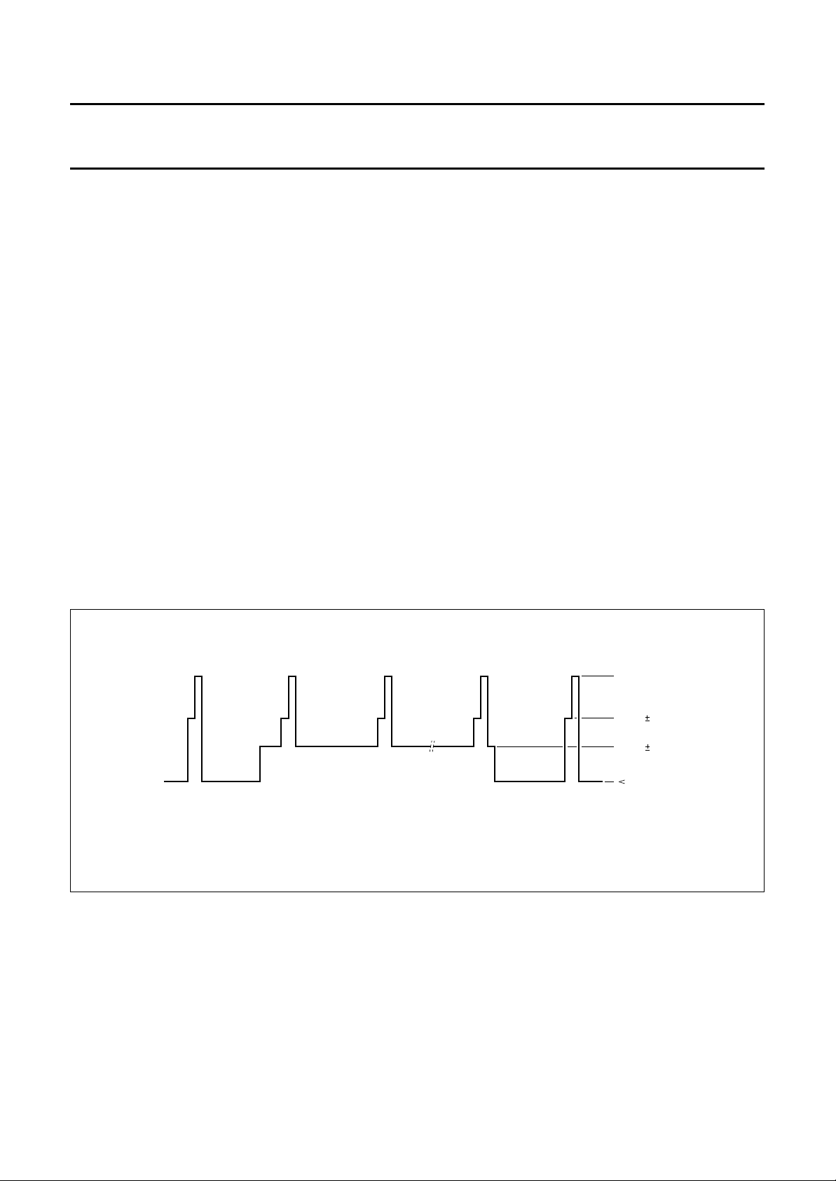
To generate a 3-level sandcastle pulse at pin 20
(see Fig.8) an external supply voltage must be connected
to pin 19.
The PAL or NTSC CVBS signal is connected to the
composite sync input (pin 29) for PLL tuning and pulse
shaping. As previously mentioned the Y input at pin 5 can
be used as the Y+SYNC input for the filtered Y+SYNC PAL
or NTSC signal, when pin 12 is at a HIGH level.
handbook, full pagewidth
Fig.8 3-level sandcastle pulse.
MSA733 - 1
V
ext
4.5 V 0.2 V
2.5 V 0.2 V
0.5 V
July 1994 10
Page 11
Philips Semiconductors Preliminary specification
SECAM encoder TDA8505
FIELD 1
3 4 5 6 7 8 9 10 11 12 13 14 15 16 17 18 19 20 21 22 23 24
21625624623622
FIELD 2
Fig.9 PLL tuning.
314 315 316 317 318 319 320 321 322 323 324 325 326 327 328 329 330 331 332 333 334 335 336 337
313312311310
July 1994 11
Page 12
Philips Semiconductors Preliminary specification
SECAM encoder TDA8505
FIELD 1
345 67 89101112131415161718192021222324
21625624623622
FIELD 2
Fig.10 Crystal tuning.
314 315 316 317 318 319 320 321 322 323 324 325 326 327 328 329 330 331 332 333 334 335 336 337
313312311310
July 1994 12
Page 13
Philips Semiconductors Preliminary specification
SECAM encoder TDA8505
Fig.11 Pulses during line blanking.
July 1994 13
Page 14
Philips Semiconductors Preliminary specification
SECAM encoder TDA8505
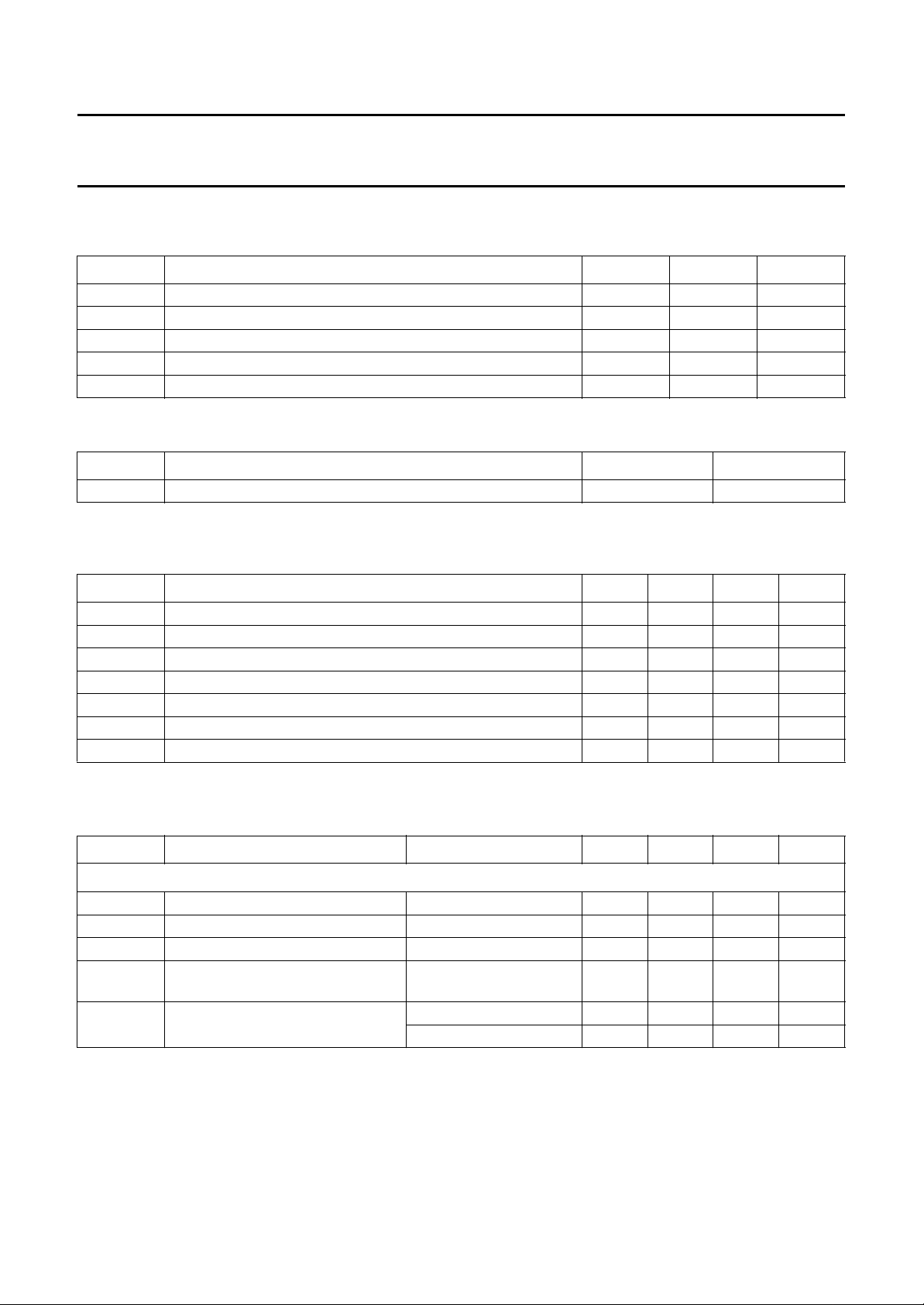
LIMITING VALUES
In accordance with the Absolute Maximum Rating System (IEC 134); all voltages referenced to V
SYMBOL PARAMETER MIN. MAX. UNIT
V
V
V
T
T
DDA
DDD
ext
stg
amb
analog supply voltage for encoder part 0 5.5 V
digital supply voltage 0 5.5 V
external supply voltage for sandcastle generation 0 13.2 V
storage temperature −65 +150 °C
operating ambient temperature −25 +70 °C
THERMAL CHARACTERISTICS
SYMBOL PARAMETER VALUE UNIT
R
th j-a
thermal resistance from junction to ambient in free air 60 K/W
DC CHARACTERISTICS
and VDD=5V; T
V
CC
=25°C; all voltages referenced to pins 10 and 30; unless otherwise specified.
amb
SSA
pin 10.
SYMBOL PARAMETER MIN. TYP. MAX. UNIT
V
V
I
DDA
I
DDD
V
P
V
DDA
DDD
ext
tot
ref
analog supply voltage for encoder part (pin 8) 4.5 5.0 5.5 V
digital supply voltage (pin 32) 4.5 5.0 5.5 V
analog supply current − 39 − mA
digital supply current − 4 − mA
external supply voltage for sandcastle generation 0 8 to 12 13.2 V
total power dissipation − 215 − mW
reference voltage output (pin 17) 2.425 2.5 2.575 V
AC CHARACTERISTICS
and VDD=5V; T
V
CC
=25°C; composite sync signal connected to pin 29; unless otherwise specified.
amb
SYMBOL PARAMETER CONDITIONS MIN. TYP. MAX. UNIT
Encoder circuit: input stage (pins 1, 3, 5, 7, 9 and 11; black level = clamping level
V
n(max)
V
n(min)
I
bias(max)
V
I
voltage from black level positive 1.2 −−V
voltage from black level negative only pins 1, 3 and 5 0.9 −−V
maximum input bias current VI=V
17
input voltage clamped input capacitor
−−1µA
− V
17
− V
connected to ground
Z
I
input clamping impedance II = 1 mA − 80 −Ω
= 1 mA − 80 −Ω
I
O
July 1994 14
Page 15
Philips Semiconductors Preliminary specification
SECAM encoder TDA8505
SYMBOL PARAMETER CONDITIONS MIN. TYP. MAX. UNIT
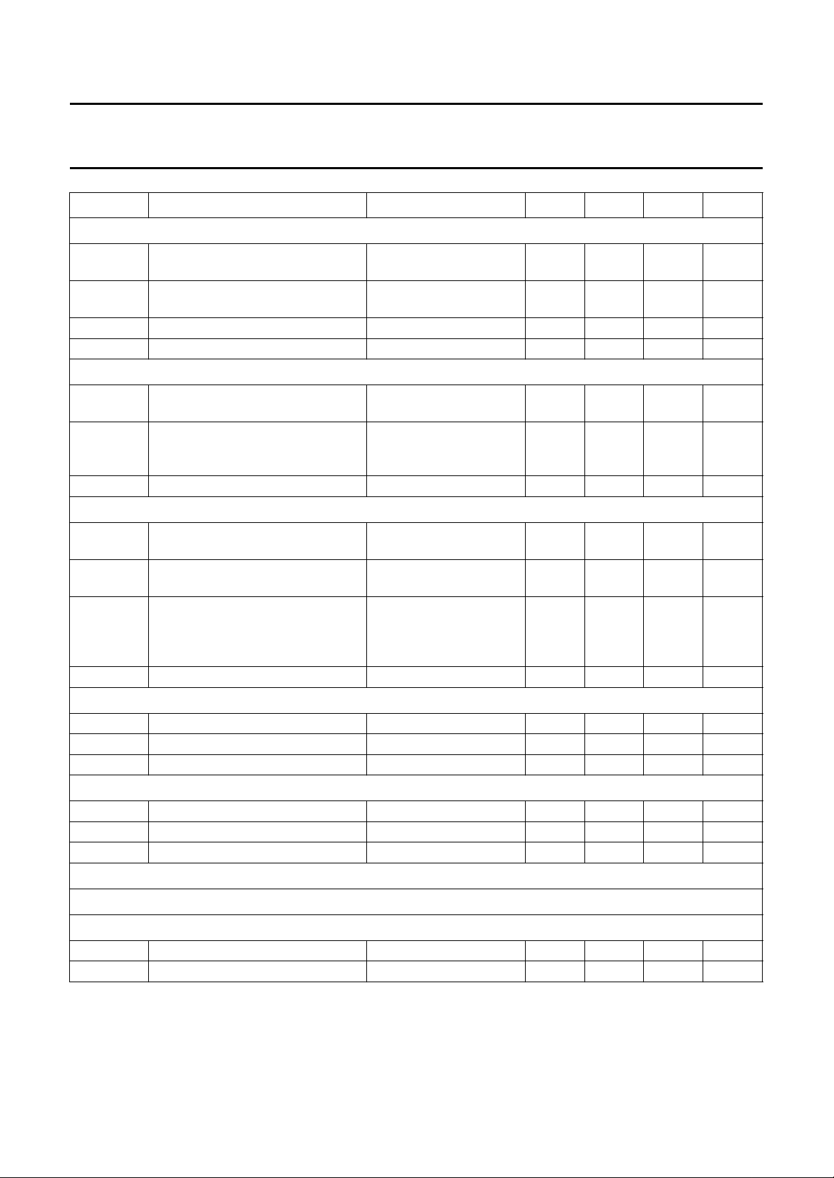
Multiplexer control (pin 2; note 1)
V
IL
LOW level input voltage Y, −(R−Y)
and −(B−Y)
V
IH
HIGH level input voltage R, G
and B
I
I
t
sw
input current −−−3µA
switching time − 50 − ns
Control input Y/Y+SYNC (pin 12)
V
IL
V
IH
I
I(max)
LOW level input voltage blanking pin 5 active;
HIGH level input voltage blanking pin 5 inactive;
maximum input current −−1µA
XTAL/PLL and VIDENT input (pin 26)
V
IL
V
IH
V
I
I
I
LOW level input voltage PLL mode; vertical
HIGH level input voltage crystal tuning; vertical
input voltage pin 26 connected to
input current −−−6µA
COLKIL input (pin 28)
V
IL
V
IH
I
I(max)
LOW level input voltage inactive 0 − 1V
HIGH level input voltage active 4 − 5V
maximum input current −−1µA
FH/2 input (pin 4)
V
IL
V
IH
I
I(max)
LOW level input voltage inactive 0 − 1V
HIGH level input voltage active 4 − 5V
maximum input current −−1µA
LF pre-emphasis (see Fig.3)
internal sync added to Y
internal sync not added
to Y
identification off
identification off
pin 17; PLL tuning;
vertical identification on;
see Fig.4
0 − 0.4 V
1 − 5V
0 − 1V
4 − 5V
0 − 1V
4 − 5V
− V
17
− V
HF pre-emphasis and bandpass (see Figs 5 and 6)
FADJ input (pin 14) resistor value for correct adjustment; see Fig.1
input sensitivity − 1.75 − kHz/mV
I
I(max)
maximum input current −−100 nA
July 1994 15
Page 16
Philips Semiconductors Preliminary specification
SECAM encoder TDA8505
SYMBOL PARAMETER CONDITIONS MIN. TYP. MAX. UNIT
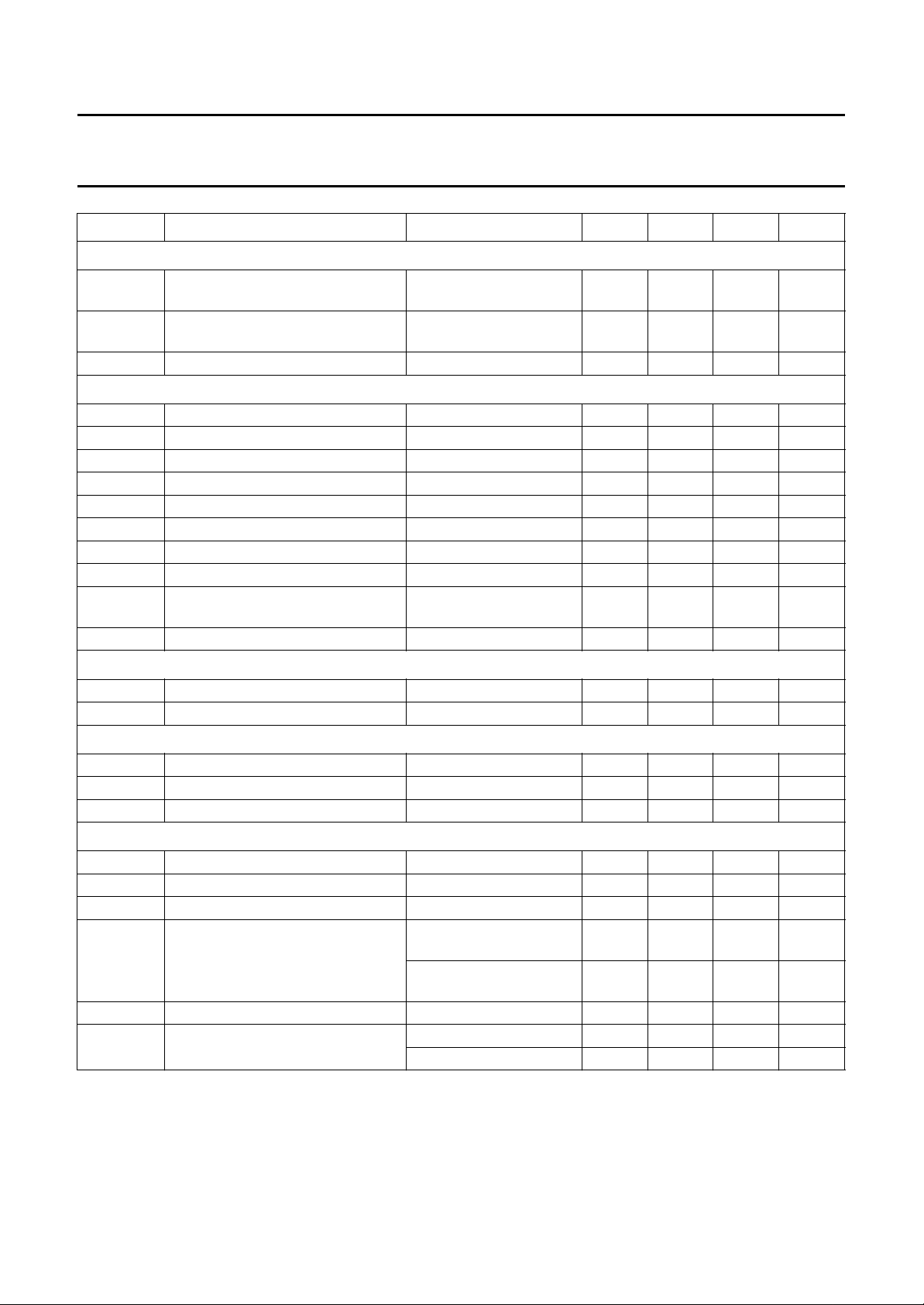
FLT output (pin 16)
V
DCL
limited DC LOW level output
voltage
V
DCH
limited DC HIGH level output
voltage
V
DC
DC level output voltage tbf 0.86 tbf V
Y+SYNC output (pin 25)
R
O
I
sink(max)
I
source(max)
V
BL
V
SYNC
V
Y
output resistance −−40 Ω
maximum sink current 200 −−µA
maximum source current 1 −−mA
black level output voltage − 1.6 − V
sync voltage amplitude 570 600 630 mV
Y voltage amplitude 1330 1400 1470 mV
B bandwidth frequency response R
t
d
t
d
group delay time tolerance RL=10kΩ; CL=10pF −−20 ns
sync delay time from
pin 29 to pin 25
t
d
Y delay time from pin 5 to pin 25 − 10 − ns
Y+SYNC input (pin 23; note 2)
I
bias
V
I(max)
input bias current −−1µA
maximum Y voltage amplitude −−1V
NOTCH output (pin 22)
R
O
V
DC
I
sink(max)
output resistance 1750 2000 2250 Ω
DC output voltage level − V
maximum sink current 300 −−µA
CHROMA output (pin 18)
I
sink(max)
I
source(max)
V
DC
∆V
DC
R
O
V
O(p-p)
maximum sink current 200 −−µA
maximum source current 1 −−mA
DC voltage level − 2.5 − V
variation of DC voltage level chrominance signal
output resistance − 120 −Ω
chrominance output voltage
amplitude (peak-to-peak value)
IO= 200 µA − 0.27 − V
II= 200 µA − 1.8 − V
=10kΩ; CL=10pF 10 −−MHz
L
220 290 360 ns
23
− V
− 5 − mV
blanked
chrominance signal not
− 5 − mV
blanked
f = 4.25 MHz − 165 − mV
f = 4.406 MHz − 205 − mV
July 1994 16
Page 17
Philips Semiconductors Preliminary specification
SECAM encoder TDA8505
SYMBOL PARAMETER CONDITIONS MIN. TYP. MAX. UNIT
FREQUENCY OF CHROMINANCE SIGNAL (NOTE 3)
f
OR
f
OB
f
max
f
min
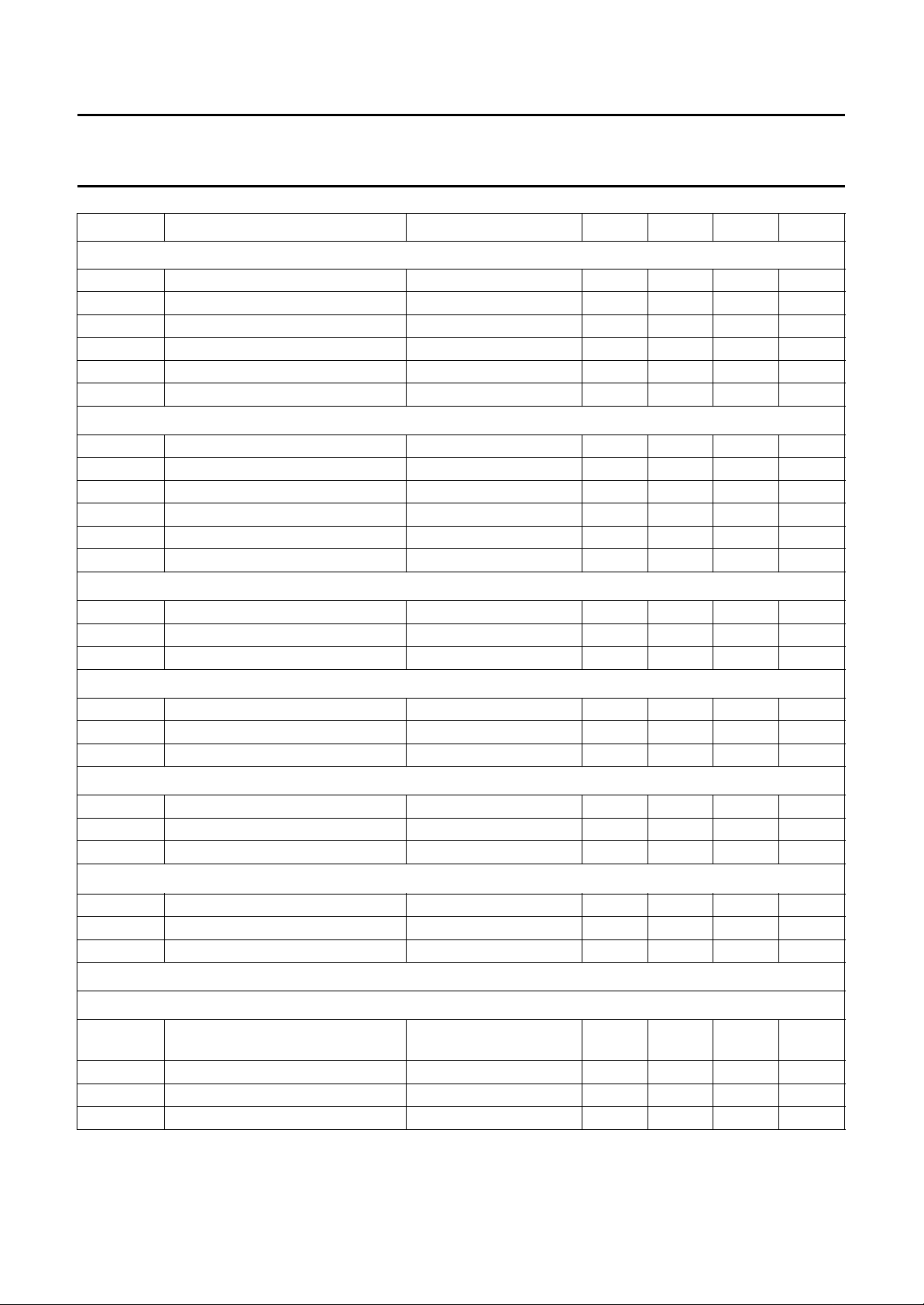
∆D'R deviation of D'R EBU bar of 75% 252 280 308 kHz
∆D'B deviation of D'B EBU bar of 75% 207 230 253 kHz
CVBS output (pin 21)
I
sink(max)
I
source(max)
V
black
G
Y
G
CHR
R
O
LPFDR output (pin 13)
V
O
I
LO
LPFDB output (pin 15)
V
O
I
LO
LPF4.4 output (pin 24)
V
O
I
LO
LPF4.25 output (pin 31; C
V
O
I
LO
VCO4.25 (pin 27; note 4)
black level of D'R − 4406 − kHz
black level of D'B − 4250 − kHz
maximum frequency 4721 4756 4791 kHz
minimum frequency 3865 3900 3935 kHz
maximum sink current 250 −−µA
maximum source current 1 −−mA
black level voltage − 1.6 − V
gain Y+SYNC (pin 23 to pin 21) − 6 − dB
gain CHROMA (pin 18 to pin 21) − 6 − dB
output resistance − 120 −Ω
DC control voltage level tbf 2.4 tbf V
control sensitivity − 0.2 − kHz/mV
output leakage current −−50 nA
DC control voltage level tbf 2.1 tbf V
control sensitivity − 1.5 − kHz/mV
output leakage current −−50 nA
DC control voltage level tbf 2.3 tbf V
control sensitivity − 1.5 − kHz/mV
output leakage current −−100 nA
= 270 pF)
ext
DC control voltage level tbf 2.3 tbf V
control sensitivity − 5.3 − kHz/mV
output leakage current −−100 nA
CS input (pin 29)
V
I(p-p)
sync pulse input amplitude
(peak-to-peak value)
slicing level − 50 − %
I
I
I
O(max)
input current − 4 −µA
maximum output current during sync − 100 −µA
July 1994 17
75 300 600 mV
Page 18
Philips Semiconductors Preliminary specification
SECAM encoder TDA8505
SYMBOL PARAMETER CONDITIONS MIN. TYP. MAX. UNIT
V
(pin 19)
ext
I
ext
SAND output (pin 20; V
I
sink(max)
I
source(max)
V
TL
Notes
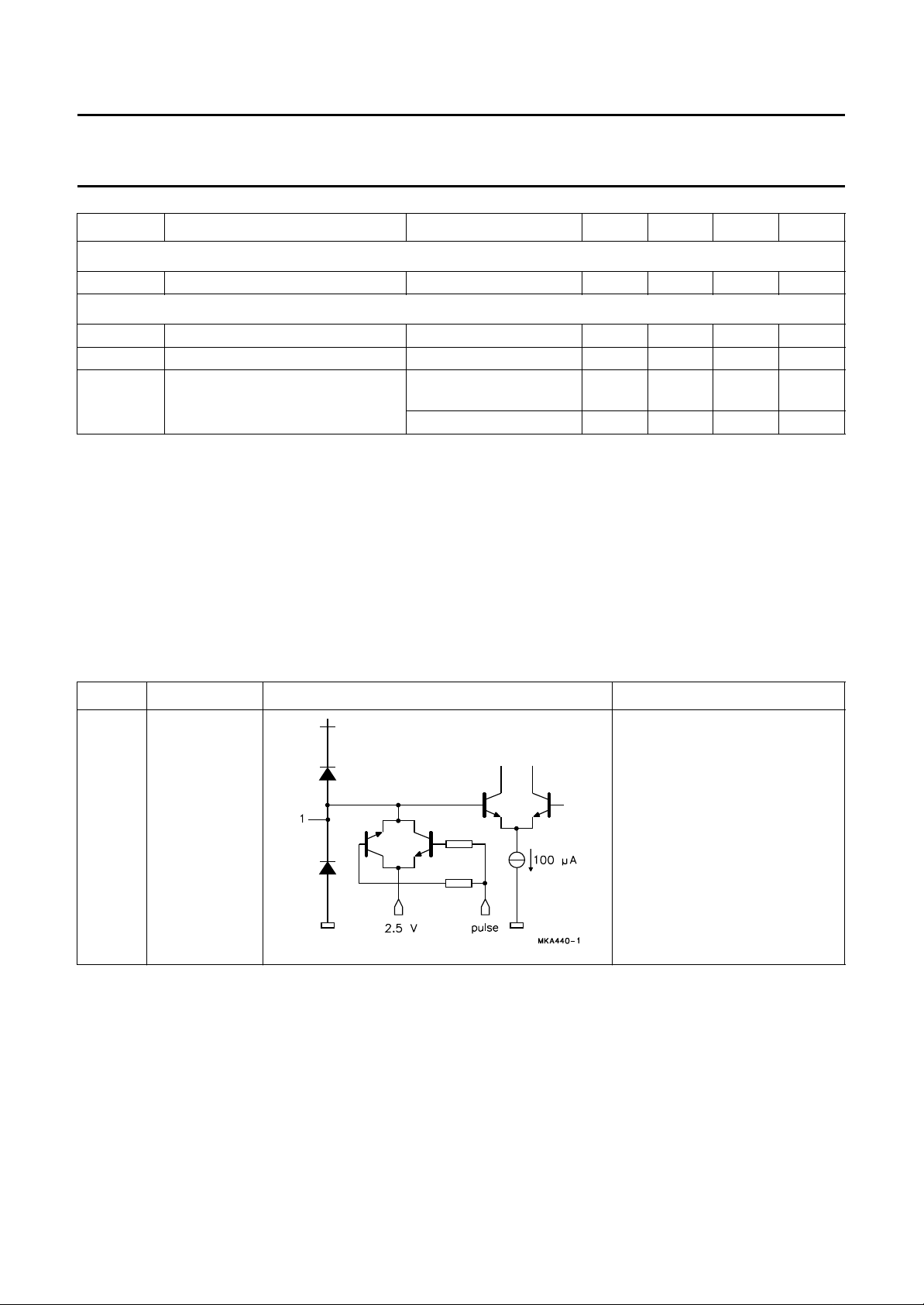
1. The threshold level of pin 2 is 700 ± 20 mV. The specification of the HIGH and LOW levels is in accordance with the
scart fast blanking.
2. The black level of input signal must be 2 V; amplitude 1 V (peak-to-peak value) nominal (Y = 700 mV,
SYNC = 300 mV).
3. The tolerances of fOR and fOB are with the printed-circuit board <±5 kHz. This value can be influenced by the print
layout.
4. The oscillator operates in series-resonance. The resonance resistance of the crystal must be <60 Ω and parallel
capacitance of the crystal <10 pF.
external supply current −−1.5 mA
= 13.2 V); see Fig.8
ext
maximum sink current 100 −−µA
maximum source current 100 −−µA
top voltage level V
< 10 V V
ext
> 10 V 10 −−V
V
ext
− 0.1−−V
ext
INTERNAL CIRCUITRY
PIN NAME CIRCUIT DESCRIPTION
1 −(R−Y) −(R−Y) input; connected via 47 nF
capacitor; 1.05 V (peak-to-peak
value) for EBU bar of 75%;
see also pins 3, 5, 7, 9 and 11
July 1994 18
Page 19
Philips Semiconductors Preliminary specification
SECAM encoder TDA8505
PIN NAME CIRCUIT DESCRIPTION
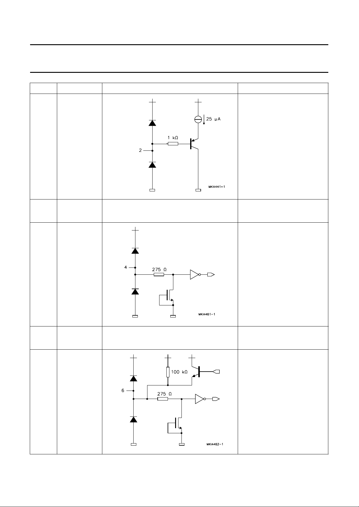
2 MCONTR multiplexer control input:
<0.4 V Y, U and V
>1 V R, G and B
3 −(B−Y) see pin 1 −(B−Y) input; connected via 47 nF
capacitor; 1.33 V (peak-to-peak
value) for EBU bar of 75%
4 FH/2 FH/2 input; forcing possibility;
when not used this pin is
connected to ground
5 Y see pin 1 Y input; connected via 47 nF
capacitor; 1 V (peak-to-peak
value) for EBU bar of 75%
6 TEST test pin; connected to V
open-circuit
July 1994 19
CC
or left
Page 20
Philips Semiconductors Preliminary specification
SECAM encoder TDA8505
PIN NAME CIRCUIT DESCRIPTION
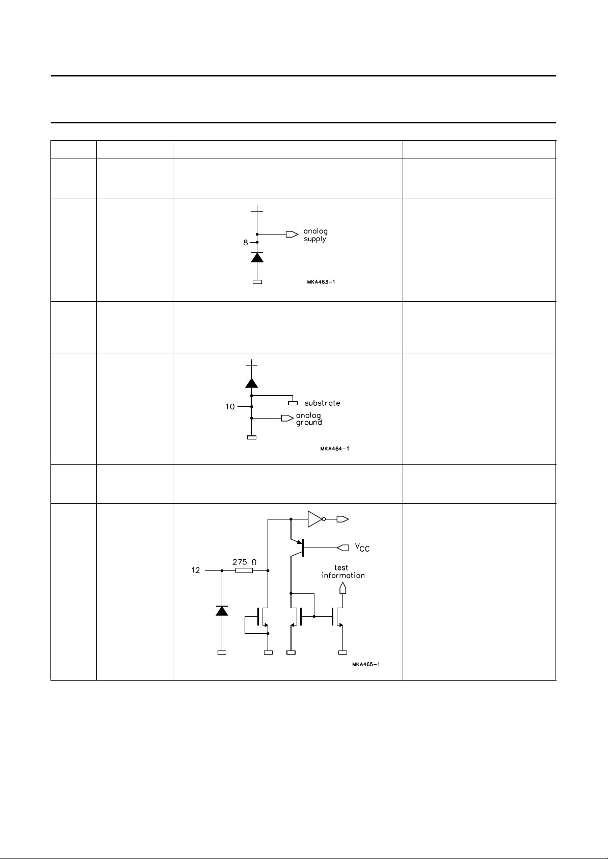
7 R see pin 1 RED input; connected via 47 nF
capacitor; 0.7 V (peak-to-peak
value) for EBU bar of 75%
8V
9 G see pin 1 GREEN input; connected via
10 V
DDA
SSA
analog supply voltage for encoder
part; 5 V nominal
47 nF capacitor; 0.7 V
(peak-to-peak value) for EBU bar
of 75%
analog ground
11 B see pin 1 BLUE input; connected via 47 nF
capacitor; 0.7 V (peak-to-peak
value) for EBU bar of 75%
12 Y/Y+SYNC control pin:
0 V Y without sync supplied to
pin 5
5 V Y with sync supplied to pin 5
July 1994 20
Page 21
Philips Semiconductors Preliminary specification
SECAM encoder TDA8505
PIN NAME CIRCUIT DESCRIPTION
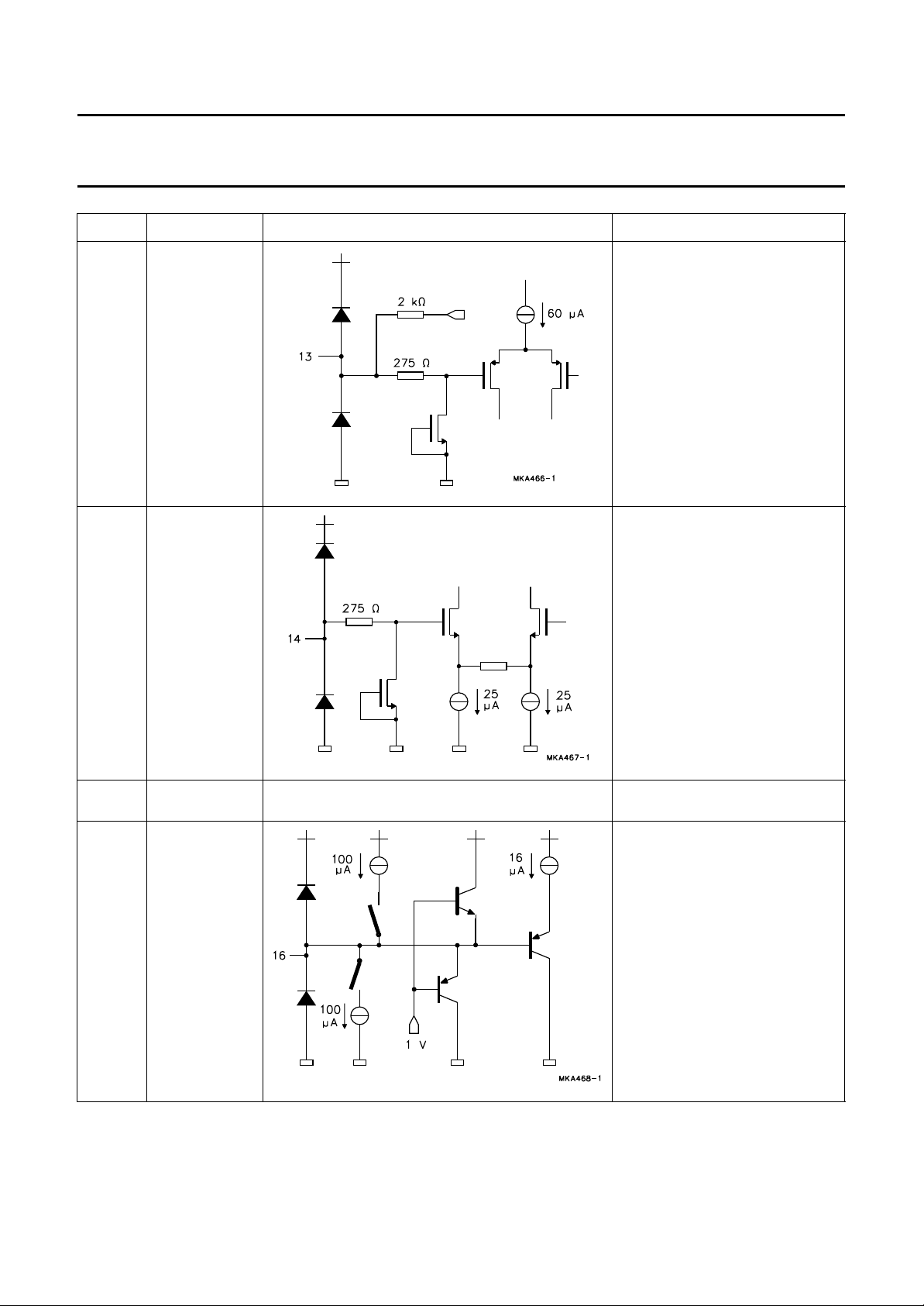
13 LPFDR modulator control loop filter with
low leakage capacitors
14 FADJ adjustment pin for 4.286 MHz:
potentiometer in series with two
resistors between ground and
pin 17
15 LPFDB see pin 13 modulator control loop filter with
low leakage capacitors
16 FLT filter control pin; 220 nF capacitor
to ground
July 1994 21
Page 22
Philips Semiconductors Preliminary specification
SECAM encoder TDA8505
PIN NAME CIRCUIT DESCRIPTION
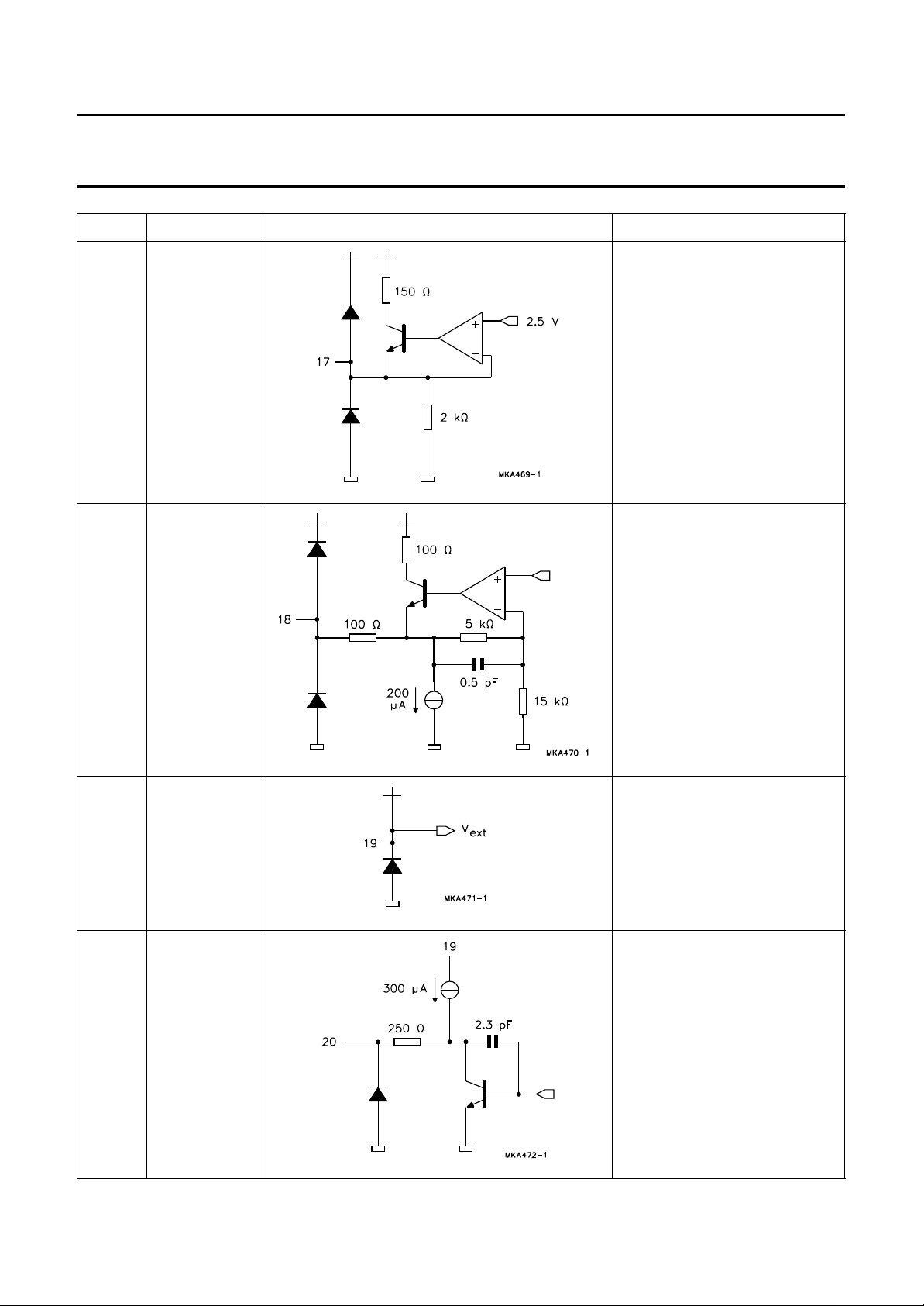
17 V
ref
18 CHROMA chrominance output
2.5 V reference voltage
decoupling with 47 µF and 22 nF
capacitors
19 V
ext
pin for external power supply, for
sandcastle pulse; V
used, the pin should be connected
to ground
20 SAND sandcastle pulse
July 1994 22
> 8 V; if not
ext
Page 23
Philips Semiconductors Preliminary specification
SECAM encoder TDA8505
PIN NAME CIRCUIT DESCRIPTION
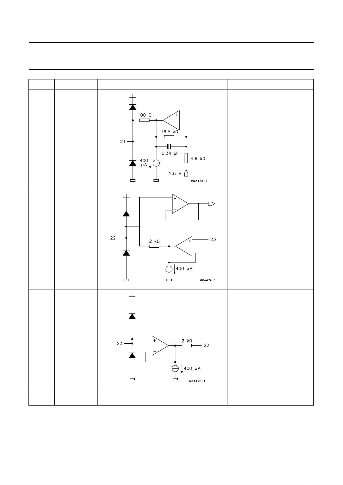
21 CVBS composite SECAM output
22 NOTCH pin for external notch filter
23 Y+SYNC IN input of the delayed Y+SYNC
signal of the delay line; black level
must be 2 V
24 LPF4.4 see pin 13 loop filter for 4.40625 MHz
reference oscillator
July 1994 23
Page 24
Philips Semiconductors Preliminary specification
SECAM encoder TDA8505
PIN NAME CIRCUIT DESCRIPTION
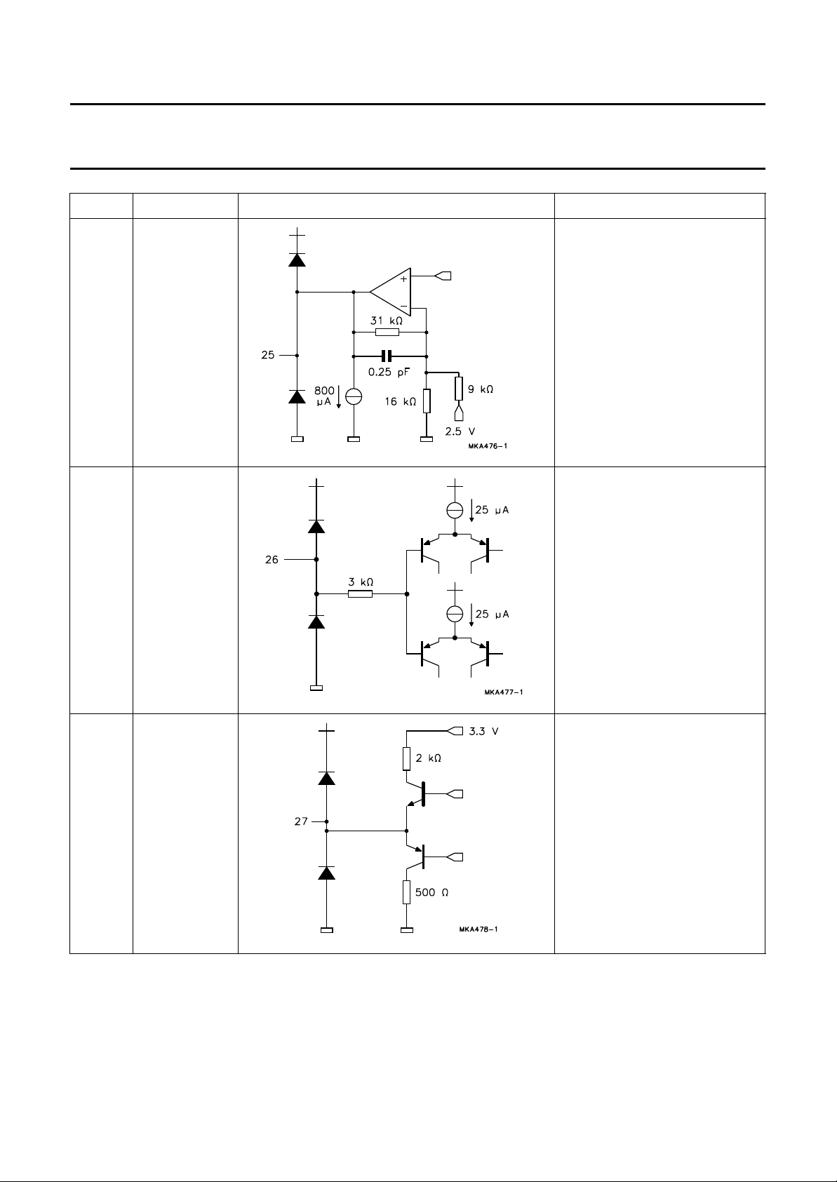
25 Y+SYNC OUT output of the delayed Y+SYNC
signal, connected to the delay line
via a resistor
26 XTAL/PLL
VIDENT
27 VCO4.25 tuning of 4.25 MHz oscillator:
control pin:
without vertical identification:
0 V PLL tuning
5 V crystal tuning
with vertical identification:
2.5 V PLL tuning
PLL tuning:
C = 270 pF to ground
crystal tuning:
crystal in series with a
capacitor to ground
external tuning:
signal via 1 nF capacitor in
series with a resistor
July 1994 24
Page 25
Philips Semiconductors Preliminary specification
SECAM encoder TDA8505
PIN NAME CIRCUIT DESCRIPTION
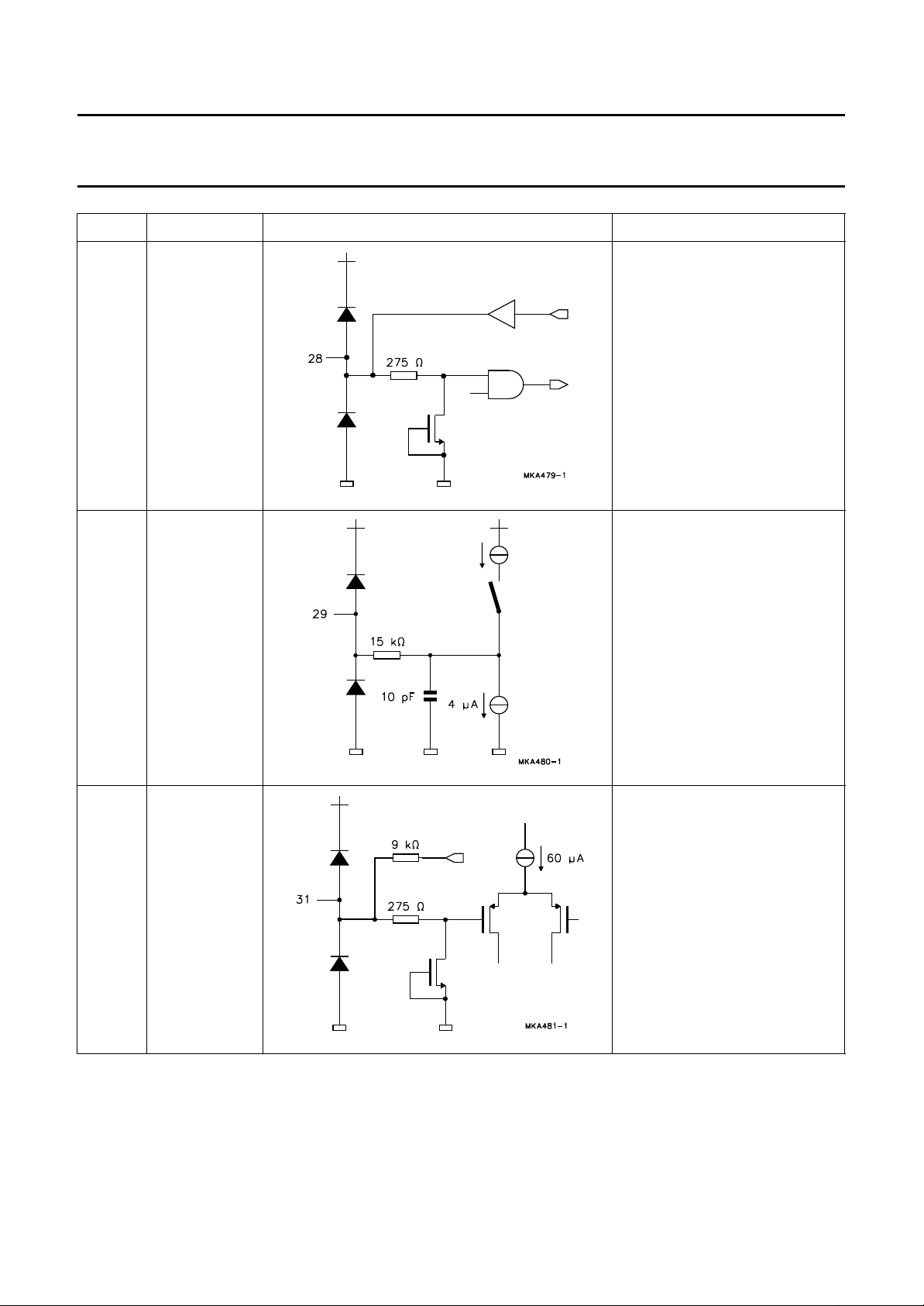
28 COLKIL colour killing input:
0 V not active
5 V active, internal D'R and D'B
are blanked
29 CS composite sync signal input;
amplitude <600 mV
(peak-to-peak value)
30 V
July 1994 25
SSD
digital ground
Page 26
Philips Semiconductors Preliminary specification
SECAM encoder TDA8505
PIN NAME CIRCUIT DESCRIPTION
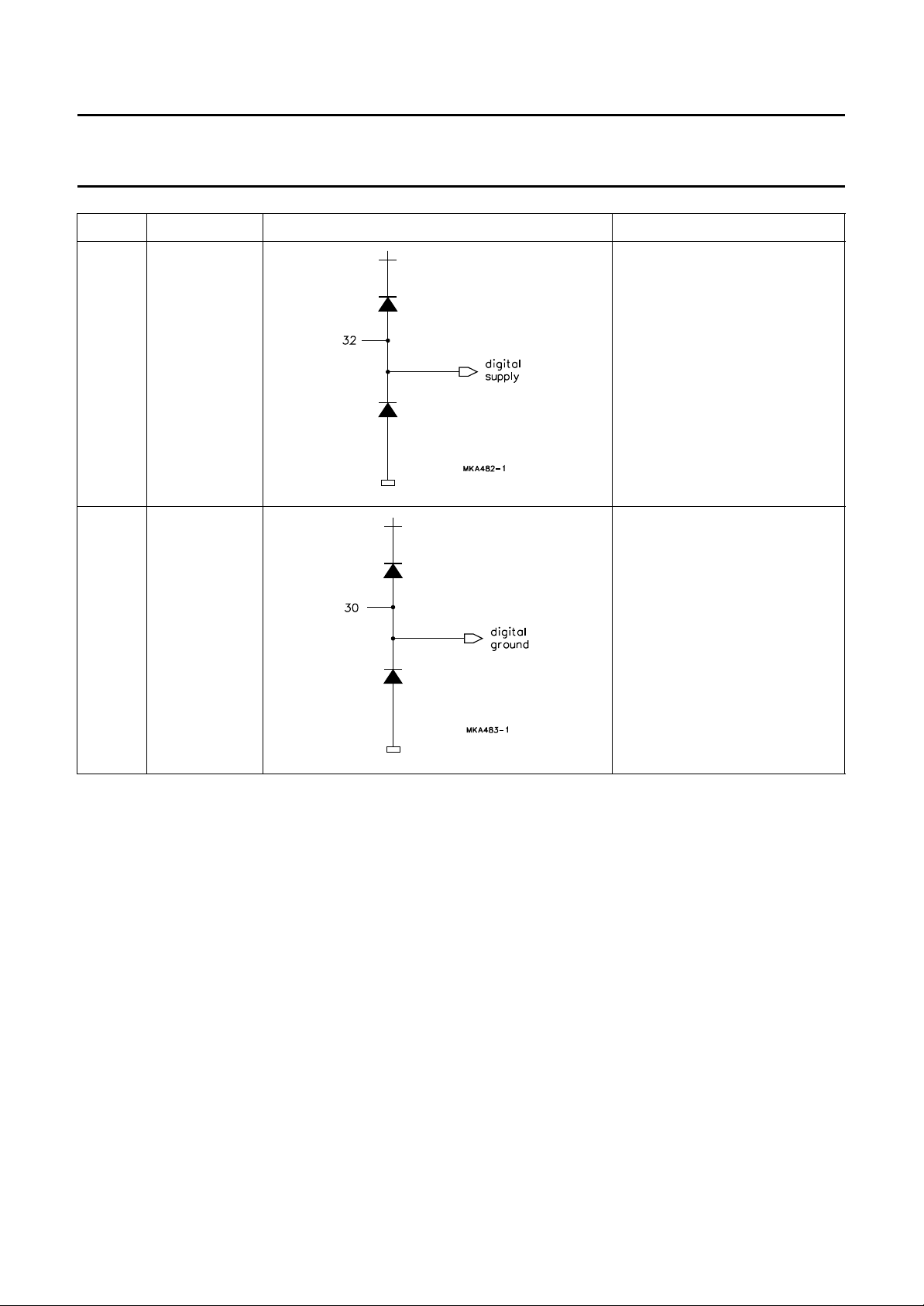
31 LPF4.25 loop filter for 4.25 MHz reference
oscillator; connected to pin 17 if
crystal or external tuning
32 V
DDD
supply voltage digital part; 5 V
nominal
July 1994 26
Page 27
Philips Semiconductors Preliminary specification
SECAM encoder TDA8505
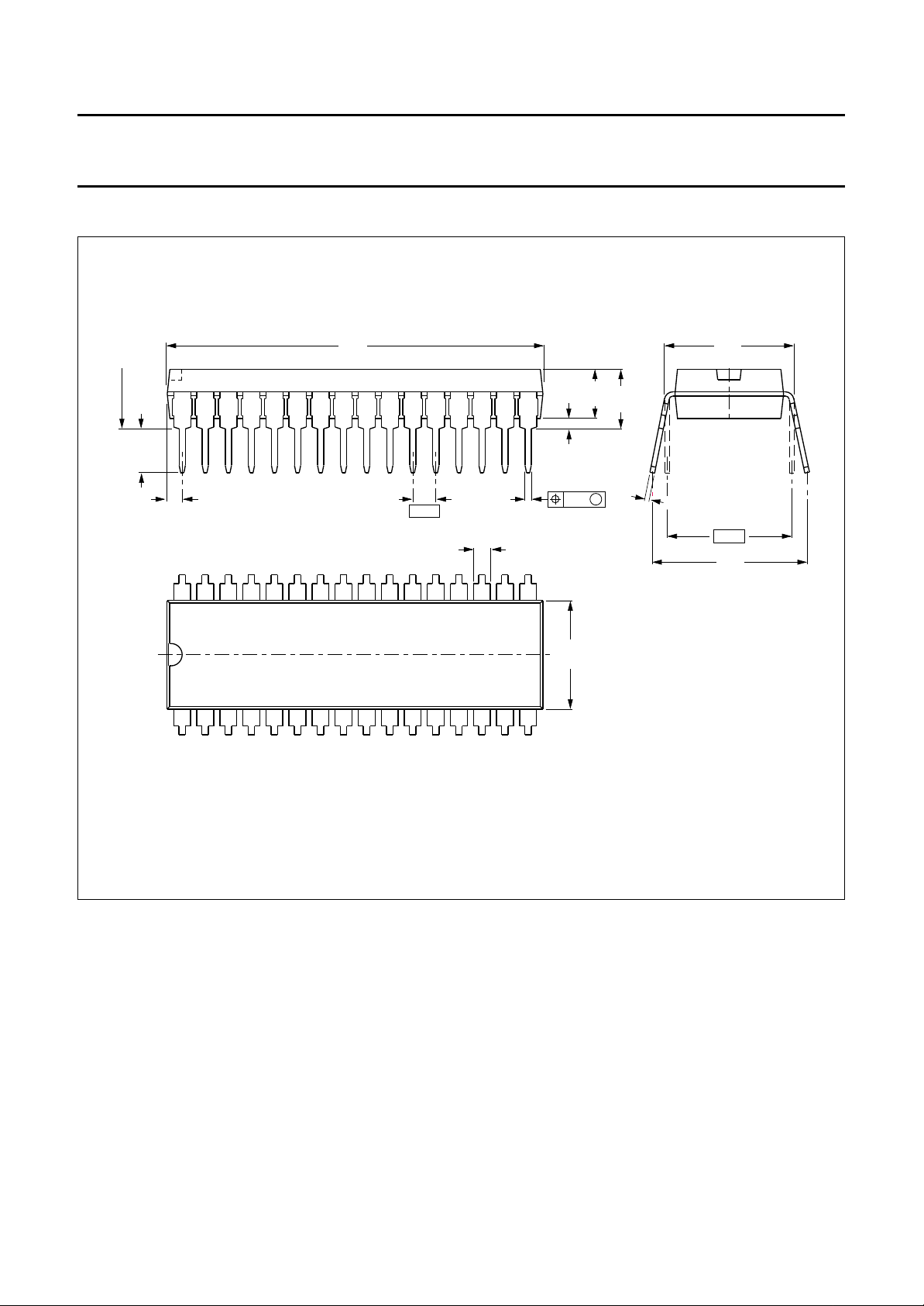
PACKAGE OUTLINE
seating plane
3.2
2.8
1.6
max
29.4
28.5
3.8
4.7
max
max
0.51
min
M
1.778
(15x)
1.3 max
32
1
0.53
max
0.18
17
9.1
8.7
16
0.32 max
10.7
10.2
10.16
12.2
10.5
MSA270
Dimensions in mm.
Fig.12 Plastic shrink dual in-line package; 32 leads (400 mil) (SDIP32; SOT232-1).
July 1994 27
Page 28

Philips Semiconductors Preliminary specification
SECAM encoder TDA8505
SOLDERING
Plastic dual in-line packages
Y DIP OR WAVE
B
The maximum permissible temperature of the solder is
260 °C; this temperature must not be in contact with the
joint for more than 5 s. The total contact time of successive
solder waves must not exceed 5 s.
The device may be mounted up to the seating plane, but
the temperature of the plastic body must not exceed the
DEFINITIONS
Data sheet status
Objective specification This data sheet contains target or goal specifications for product development.
Preliminary specification This data sheet contains preliminary data; supplementary data may be published later.
Product specification This data sheet contains final product specifications.
Limiting values
Limiting values given are in accordance with the Absolute Maximum Rating System (IEC 134). Stress above one or
more of the limiting values may cause permanent damage to the device. These are stress ratings only and operation
of the device at these or at any other conditions above those given in the Characteristics sections of the specification
is not implied. Exposure to limiting values for extended periods may affect device reliability.
specified storage maximum. If the printed-circuit board has
been pre-heated, forced cooling may be necessary
immediately after soldering to keep the temperature within
the permissible limit.
EPAIRING SOLDERED JOINTS
R
Apply a low voltage soldering iron below the seating plane
(or not more than 2 mm above it). If its temperature is
below 300 °C, it must not be in contact for more than 10 s;
if between 300 and 400 °C, for not more than 5 s.
Application information
Where application information is given, it is advisory and does not form part of the specification.
LIFE SUPPORT APPLICATIONS
These products are not designed for use in life support appliances, devices, or systems where malfunction of these
products can reasonably be expected to result in personal injury. Philips customers using or selling these products for
use in such applications do so at their own risk and agree to fully indemnify Philips for any damages resulting from such
improper use or sale.
July 1994 28
Page 29

Philips Semiconductors Preliminary specification
SECAM encoder TDA8505
NOTES
July 1994 29
Page 30

Philips Semiconductors Preliminary specification
SECAM encoder TDA8505
NOTES
July 1994 30
Page 31

Philips Semiconductors Preliminary specification
SECAM encoder TDA8505
NOTES
July 1994 31
Page 32

Philips Semiconductors – a worldwide company
Argentina: IEROD, Av. Juramento 1992 - 14.b, (1428)
BUENOS AIRES, Tel. (541)786 7633, Fax. (541)786 9367
Australia: 34 Waterloo Road, NORTH RYDE, NSW 2113,
Tel. (02)805 4455, Fax. (02)805 4466
Austria: Triester Str. 64, A-1101 WIEN, P.O. Box 213,
Tel. (01)60 101-1236, Fax. (01)60 101-1211
Belgium: Postbus 90050, 5600 PB EINDHOVEN, The Netherlands,
Tel. (31)40 783 749, Fax. (31)40 788 399
Brazil: Rua do Rocio 220 - 5
CEP: 04552-903-SÃO PAULO-SP, Brazil.
P.O. Box 7383 (01064-970).
Tel. (011)821-2333, Fax. (011)829-1849
Canada: INTEGRATED CIRCUITS:
Tel. (800)234-7381, Fax. (708)296-8556
DISCRETE SEMICONDUCTORS: 601 Milner Ave,
SCARBOROUGH, ONTARIO, M1B 1M8,
Tel. (0416)292 5161 ext. 2336, Fax. (0416)292 4477
Chile: Av. Santa Maria 0760, SANTIAGO,
Tel. (02)773 816, Fax. (02)777 6730
Colombia: IPRELENSO LTDA, Carrera 21 No. 56-17,
77621 BOGOTA, Tel. (571)249 7624/(571)217 4609,
Fax. (571)217 4549
Denmark: Prags Boulevard 80, PB 1919, DK-2300 COPENHAGEN S,
Tel. (032)88 2636, Fax. (031)57 1949
Finland: Sinikalliontie 3, FIN-02630 ESPOO,
Tel. (9)0-50261, Fax. (9)0-520971
France: 4 Rue du Port-aux-Vins, BP317,
92156 SURESNES Cedex,
Tel. (01)4099 6161, Fax. (01)4099 6427
Germany: PHILIPS COMPONENTS UB der Philips G.m.b.H.,
P.O. Box 10 63 23, 20043 HAMBURG,
Tel. (040)3296-0, Fax. (040)3296 213.
Greece: No. 15, 25th March Street, GR 17778 TAVROS,
Tel. (01)4894 339/4894 911, Fax. (01)4814 240
Hong Kong: PHILIPS HONG KONG Ltd., Components Div.,
6/F Philips Ind. Bldg., 24-28 Kung Yip St., KWAI CHUNG, N.T.,
Tel. (852)424 5121, Fax. (852)428 6729
India: Philips INDIA Ltd, Components Dept,
Shivsagar Estate, A Block ,
Dr. Annie Besant Rd. Worli, Bombay 400 018
Tel. (022)4938 541, Fax. (022)4938 722
Indonesia: Philips House, Jalan H.R. Rasuna Said Kav. 3-4,
P.O. Box 4252, JAKARTA 12950,
Tel. (021)5201 122, Fax. (021)5205 189
Ireland: Newstead, Clonskeagh, DUBLIN 14,
Tel. (01)640 000, Fax. (01)640 200
Italy: PHILIPS COMPONENTS S.r.l.,
Viale F. Testi, 327, 20162 MILANO,
Tel. (02)6752.3302, Fax. (02)6752 3300.
Japan: Philips Bldg 13-37, Kohnan 2-chome, Minato-ku, TOKYO 108,
Tel. (03)3740 5028, Fax. (03)3740 0580
Korea: (Republic of) Philips House, 260-199 Itaewon-dong,
Yongsan-ku, SEOUL, Tel. (02)794-5011, Fax. (02)798-8022
Malaysia: No. 76 Jalan Universiti, 46200 PETALING JAYA,
SELANGOR, Tel. (03)750 5214, Fax. (03)757 4880
Mexico: Philips Components, 5900 Gateway East, Suite 200,
EL PASO, TX 79905, Tel. 9-5(800)234-7381, Fax. (708)296-8556
Netherlands: Postbus 90050, 5600 PB EINDHOVEN, Bldg. VB
Tel. (040)783749, Fax. (040)788399
New Zealand: 2 Wagener Place, C.P.O. Box 1041, AUCKLAND,
Tel. (09)849-4160, Fax. (09)849-7811
th
floor, Suite 51,
Norway: Box 1, Manglerud 0612, OSLO,
Tel. (022)74 8000, Fax. (022)74 8341
Pakistan: Philips Electrical Industries of Pakistan Ltd.,
Exchange Bldg. ST-2/A, Block 9, KDA Scheme 5, Clifton,
KARACHI 75600, Tel. (021)587 4641-49,
Fax. (021)577035/5874546.
Philippines: PHILIPS SEMICONDUCTORS PHILIPPINES Inc,
106 Valero St. Salcedo Village, P.O. Box 2108 MCC, MAKATI,
Metro MANILA, Tel. (02)810 0161, Fax. (02)817 3474
Portugal: PHILIPS PORTUGUESA, S.A.,
Rua dr. António Loureiro Borges 5, Arquiparque - Miraflores,
Apartado 300, 2795 LINDA-A-VELHA,
Tel. (01)14163160/4163333, Fax. (01)14163174/4163366.
Singapore: Lorong 1, Toa Payoh, SINGAPORE 1231,
Tel. (65)350 2000, Fax. (65)251 6500
South Africa: S.A. PHILIPS Pty Ltd., Components Division,
195-215 Main Road Martindale, 2092 JOHANNESBURG,
P.O. Box 7430 Johannesburg 2000,
Tel. (011)470-5911, Fax. (011)470-5494.
Spain: Balmes 22, 08007 BARCELONA,
Tel. (03)301 6312, Fax. (03)301 42 43
Sweden: Kottbygatan 7, Akalla. S-164 85 STOCKHOLM,
Tel. (0)8-632 2000, Fax. (0)8-632 2745
Switzerland: Allmendstrasse 140, CH-8027 ZÜRICH,
Tel. (01)488 2211, Fax. (01)481 77 30
Taiwan: PHILIPS TAIWAN Ltd., 23-30F, 66, Chung Hsiao West
Road, Sec. 1. Taipeh, Taiwan ROC, P.O. Box 22978,
TAIPEI 100, Tel. (02)388 7666, Fax. (02)382 4382.
Thailand: PHILIPS ELECTRONICS (THAILAND) Ltd.,
209/2 Sanpavuth-Bangna Road Prakanong,
Bangkok 10260, THAILAND,
Tel. (662)398-0141, Fax. (662)398-3319.
Turkey:Talatpasa Cad. No. 5, 80640 GÜLTEPE/ISTANBUL,
Tel. (0212)279 2770, Fax. (0212)269 3094
United Kingdom: Philips Semiconductors Limited, P.O. Box 65,
Philips House, Torrington Place, LONDON, WC1E 7HD,
Tel. (071)436 41 44, Fax. (071)323 03 42
United States:INTEGRATED CIRCUITS:
811 East Arques Avenue, SUNNYVALE, CA 94088-3409,
Tel. (800)234-7381, Fax. (708)296-8556
DISCRETE SEMICONDUCTORS: 2001 West Blue Heron Blvd.,
P.O. Box 10330, RIVIERA BEACH, FLORIDA 33404,
Tel. (800)447-3762 and (407)881-3200, Fax. (407)881-3300
Uruguay: Coronel Mora 433, MONTEVIDEO,
Tel. (02)70-4044, Fax. (02)92 0601
For all other countries apply to: Philips Semiconductors,
International Marketing and Sales, Building BAF-1,
P.O. Box 218, 5600 MD, EINDHOVEN, The Netherlands,
Telex 35000 phtcnl, Fax. +31-40-724825
SCD32 © Philips Electronics N.V. 1994
All rights are reserved. Reproduction in whole or in part is prohibited without the
prior written consent of the copyright owner.
The information presented in this document does not form part of any quotation
or contract, is believed to be accurate and reliable and may be changed without
notice. No liability will be accepted by the publisher for any consequence of its
use. Publication thereof does not convey nor imply any license under patent- or
other industrial or intellectual property rights.
Printed in The Netherlands
533061/1500/03/pp32 Date of release: July 1994
Document order number: 9397 736 70011
Philips Semiconductors
 Loading...