

Page 1

DATA SH EET
Product specification
File under Integrated Circuits, IC02
September 1992
INTEGRATED CIRCUITS
TDA8424
Hi-Fi stereo audio processor;
I
2
C-bus
Page 2
September 1992 2
Philips Semiconductors Product specification
Hi-Fi stereo audio processor; I2C-bus
TDA8424
FEATURES
• Mode selector
• Spatial stereo, stereo and forced mono switch
• Volume and balance control
• Bass, treble and mute control
• Power supply with power-on reset
GENERAL DESCRIPTION
The TDA8424 is monolithic bipolar integrated stereo
sound circuit with a loudspeaker channel facility, digitally
controlled via the I
2
C-bus for application in hi-fi audio and
television sound.
QUICK REFERENCE DATA
ORDERING INFORMATION
Note
1. SOT146-1; 1996 December 3.
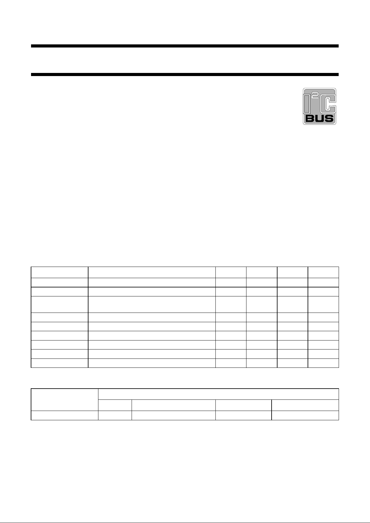
SYMBOL PARAMETER MIN. TYP. MAX. UNIT
V
CC
positive supply voltage (pin 4) 10.8 12.0 13.2 V
V
I
input signal handling 2 −−V
V
i
input sensitivity with full power at the output
stage
− 300 − mV
(S+N)/N signal plus noise-to-noise ratio − 86 − dB
THD total harmonic distortion − 0.05 − %
α
cs
channel separation − 80 − dB
G
vol
volume control range −64 −+6dB
G
tre
treble control range −12 −+12 dB
G
bass
bass control range −12 −+15 dB
EXTENDED TYPE
NUMBER
PACKAGE
PINS PIN POSITION MATERIAL CODE
TDA8424 20 DIL plastic SOT146
(1)
Page 3
September 1992 3
Philips Semiconductors Product specification
Hi-Fi stereo audio processor; I2C-bus
TDA8424
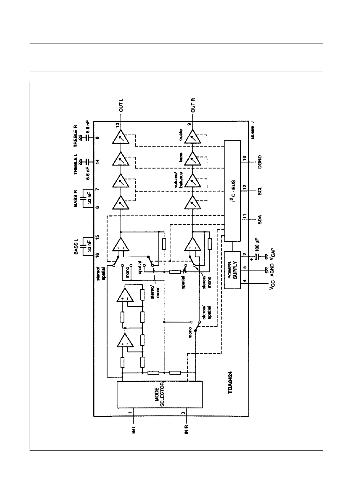
Fig.1 Block diagram.
Page 4
September 1992 4
Philips Semiconductors Product specification
Hi-Fi stereo audio processor; I2C-bus
TDA8424
PINNING
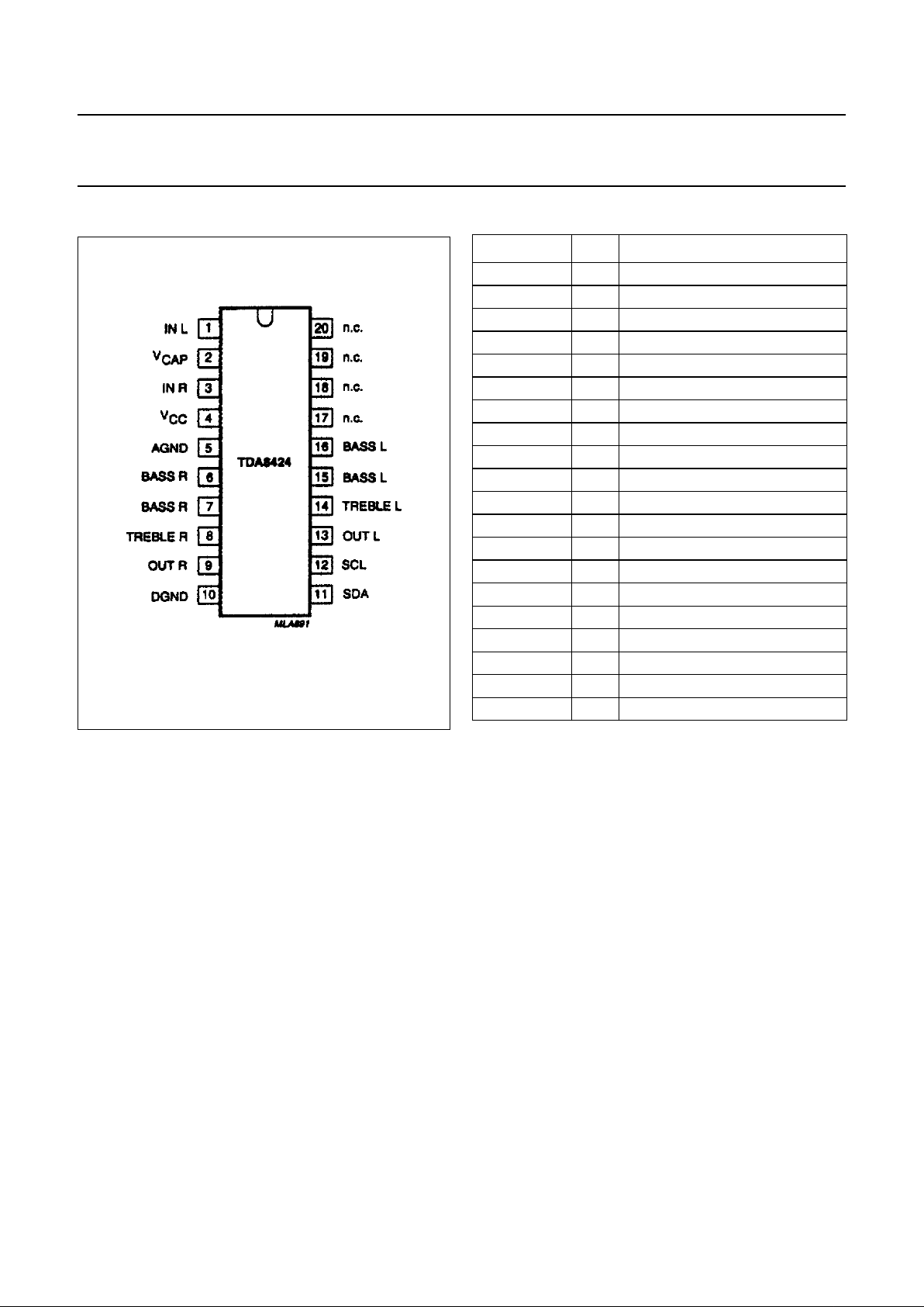
Fig.2 Pin configuration.
SYMBOL PIN DESCRIPTION
IN L 1 left channel input
V
CAP
2 decoupling capacitor
IN R 3 right channel input
V
CC
4 positive supply voltage
AGND 5 analog ground
BASS R 6 right channel bass control
BASS R 7 right channel bass control
TREBLE R 8 right channel treble control
OUT R 9 right channel output
DGND 10 digital ground
SDA 11 serial data input/output
SCL 12 serial clock input
OUT L 13 left channel output
TREBLE L 14 left channel treble control
BASS L 15 left channel bass control
BASS L 16 left channel bass control
n.c. 17 not connected
n.c. 18 not connected
n.c. 19 not connected
n.c. 20 not connected
Page 5
September 1992 5
Philips Semiconductors Product specification
Hi-Fi stereo audio processor; I2C-bus
TDA8424
FUNCTIONAL DESCRIPTION
Mode selector
The mode selector selects between stereo, sound A and
sound B (in the event of bi-lingual transmission) for OUT R
and OUT L.
Volume control and balance
The volume control consists of two stages (left and right).
In each part the gain can be adjusted between +6 dB and
−64 dB in steps of 2 dB. An additional step allows an
attenuation of ≥ 80 dB. Both parts can be controlled
independently over the whole range, which allows the
balance to be varied by controlling the volume of left and
right output channels.
Stereo, spatial stereo and forced mono mode
It is possible to select three modes: stereo, spatial stereo
or forced mono. The spatial stereo mode handles stereo
transmissions and the forced mono can be used in the
event of stereo signals.
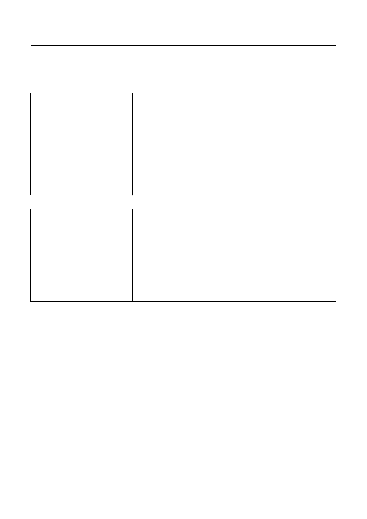
Bass control
The bass control can be switched from an emphasis of
15 dB to an attenuation of 12 dB for low frequencies in
steps of 3 dB.
Treble control
The treble control stage can be switched
from +12 dB to −12 dB in steps of 3 dB.
Bias and power supply
The TDA8424 includes a bias and power supply stage,
which generates a voltage of 0.5 V
CC
with a low output
impedance and injector currents for the logic part.
Power-on reset
The on-chip power-on reset circuit sets the mute bit to
active, which mutes both parts of the treble amplifier. The
muting can be switched by transmission of the mute bit.
I
2
C-bus receiver and data handling
B
US SPECIFICATION
The TDA8424 is controlled via the 2-wire I2C-bus by a
microcontroller.
The two wires (SDA - serial data, SCL - serial clock) carry
information between the devices connected to the bus.
Both SDA and SCL are bi-directional lines, connected to a
positive supply voltage via a pull-up resistor.
When the bus is free both lines are HIGH.
The data on the SDA line must be stable during the HIGH
period of the clock. The HIGH or LOW state of the data line
can only change when the clock on the SCL line is LOW.
The set-up and hold times are specified in the AC
CHARACTERISTICS.
A HIGH-to-LOW transition of the SDA line while SCL is
HIGH is defined as a start condition.
A LOW-to-HIGH transition of the SDA line while SCL is
HIGH is defined as a stop condition.
The bus receiver will be reset by the reception of a start
condition. The bus is considered to be busy after the start
condition.
The bus is considered free again after a stop condition.
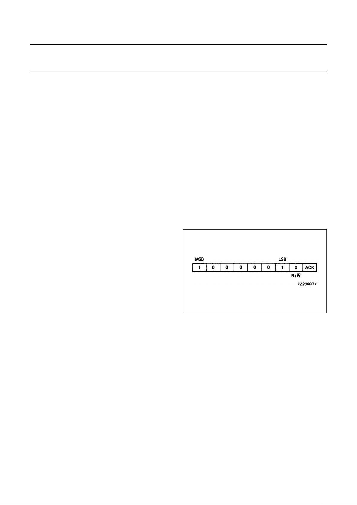
Module address
Data transmission to the TDA8424 starts with the module
address MAD.
Subaddress
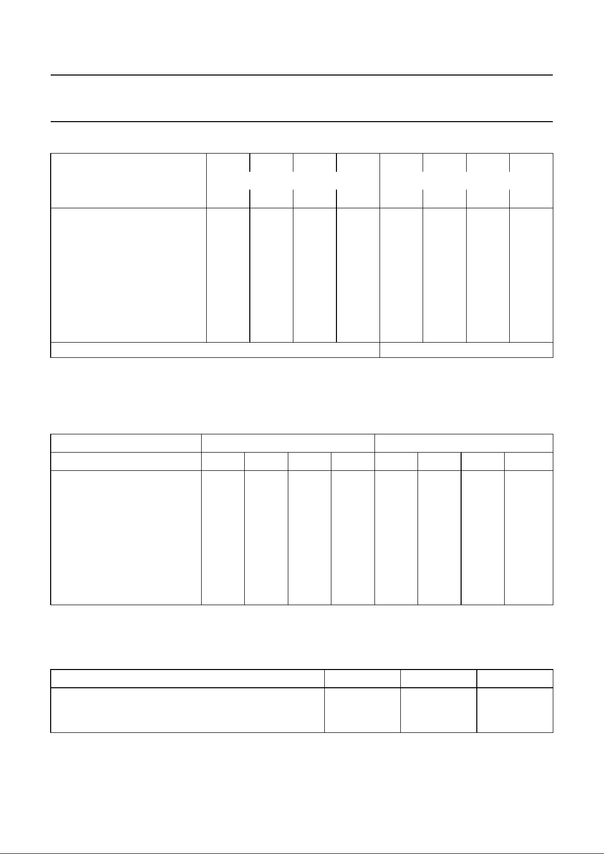
After the module address byte a second byte is used to
select the following functions:
• Volume left, volume right, bass, treble and switch
functions
The subaddress SAD is stored within the TDA8424. Table
1 defines the coding of the second byte after the module
address MAD.
The automatic increment feature of the slave address
enables a quick slave receiver initialization, within one
transmission, by the I
2
C-bus controller (see Fig.5).
Fig.3 TDA8424 module address.
Page 6
September 1992 6
Philips Semiconductors Product specification
Hi-Fi stereo audio processor; I2C-bus
TDA8424
Table 1 Second byte after module address MAD
Definition of 3rd byte
A third byte is used to transmit data to the TDA8424. Table 2 defines the coding of the third byte after module address
MAD and subaddress SAD.
Table 2 Third byte after module address MAD and subaddress SAD
Truth tables
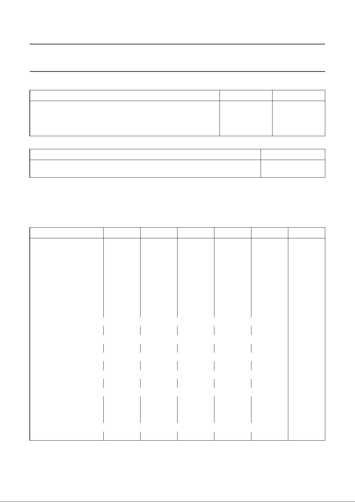
Tables 3, 4 and 5 are truth tables for the switch functions
Table 3 Mode selector
Note
1. Must be set to logic 1
FUNCTION
128 64 32 16 8 4 2 1
MSB LSB
76543210
Volume left 0 0 0 0 0 0 0 0
Volume right 0 0 0 0 0 0 0 1
Bass 0 0 0 0 0 0 1 0
Treble 0 0 0 0 0 0 1 1
00000000
00000000
00000000
00000000
Switch functions 0 0 0 0 1 0 0 0
subaddress SAD
MSB LSB
FUNCTION 7 6 5 4 3 2 1 0
Volume left VL 1 1 V05 V04 V03 V02 V01 V00
Volume right VR 1 1 V15 V14 V13 V12 V11 V10
Bass BA 1 1 1 1 BA3 BA2 BA1 BA0
Treble TR 1 1 1 1 TR3 TR2 TR1 TR0
1111111 1
1111111 1
1111111 1
1111111 1
Switch functions S1 1 1 MU EFL STL ML1 ML0 1
FUNCTION ML1 ML0 IS
Stereo 1 1 1
(1)
Sound A 0 1 1
(1)
Sound B 1 0 1
(1)
Page 7
September 1992 7
Philips Semiconductors Product specification
Hi-Fi stereo audio processor; I2C-bus
TDA8424
Table 4 Stereo/spatial stereo/forced mono
Table 5 Mute (see note 1)
Note
1. POR = Power-on reset.
Tables 6, 7 and 8 are truth tables for the volume, bass and treble controls
Table 6 Volume control
CHOICE STL EFL
Spatial stereo 1 1
Stereo 10
Forbidden status 0 1
Forced mono 0 0
MUTE MU
Active; automatic after POR 1
Not active 0
2 dB/STEP (dB) V × 5V×4V×3V×2V×1V×0
6 111111
4 111110
2 111101
0 111100
−2 111011
−4 111010
−6 111001
−8 111000
−10 110111
−20 110010
−30 101101
−40 101000
−50 100011
−60 011110
−62 011101
−64 011100
−80 011011
Page 8
September 1992 8
Philips Semiconductors Product specification
Hi-Fi stereo audio processor; I2C-bus
TDA8424
Table 7 Bass control
Table 8 Treble control
3 dB/STEP (dB) BA3 BA2 BA1 BA0
15 1011
12 1010
9 1001
6 1000
3 0111
0 0110
−3 0101
−6 0100
−9 0011
−12 0010
3 dB/STEP (dB) TR3 TR2 TR1 TR0
12 1010
9 1001
6 1000
3 0111
0 0110
−3 0101
−6 0100
−9 0011
−12 0010
Page 9
September 1992 9
Philips Semiconductors Product specification
Hi-Fi stereo audio processor; I2C-bus
TDA8424
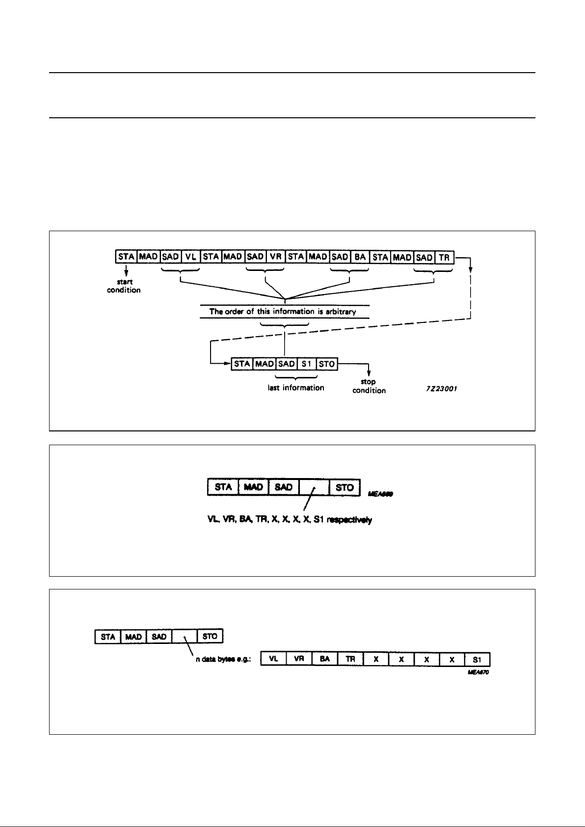
Sequence of data transmission
After a power-on reset all five functions have to be adjusted with five data transmissions. It is recommended that data
information for switch functions are transmitted last because all functions have to be adjusted when the muting is
switched off. The sequence of transmission of other data information is not critical.
The order of data transmission is shown in Figures 4 and 6. The number of data transmissions is unrestricted but before
each data byte the module address MAD and the correct subaddress SAD is required.
Fig.4 Data transmission after a power-on reset.
Fig.5 Data transmission after a power-on reset with auto increment.
Fig.6 Data transmission except after a power-on reset.
Page 10
September 1992 10
Philips Semiconductors Product specification
Hi-Fi stereo audio processor; I2C-bus
TDA8424
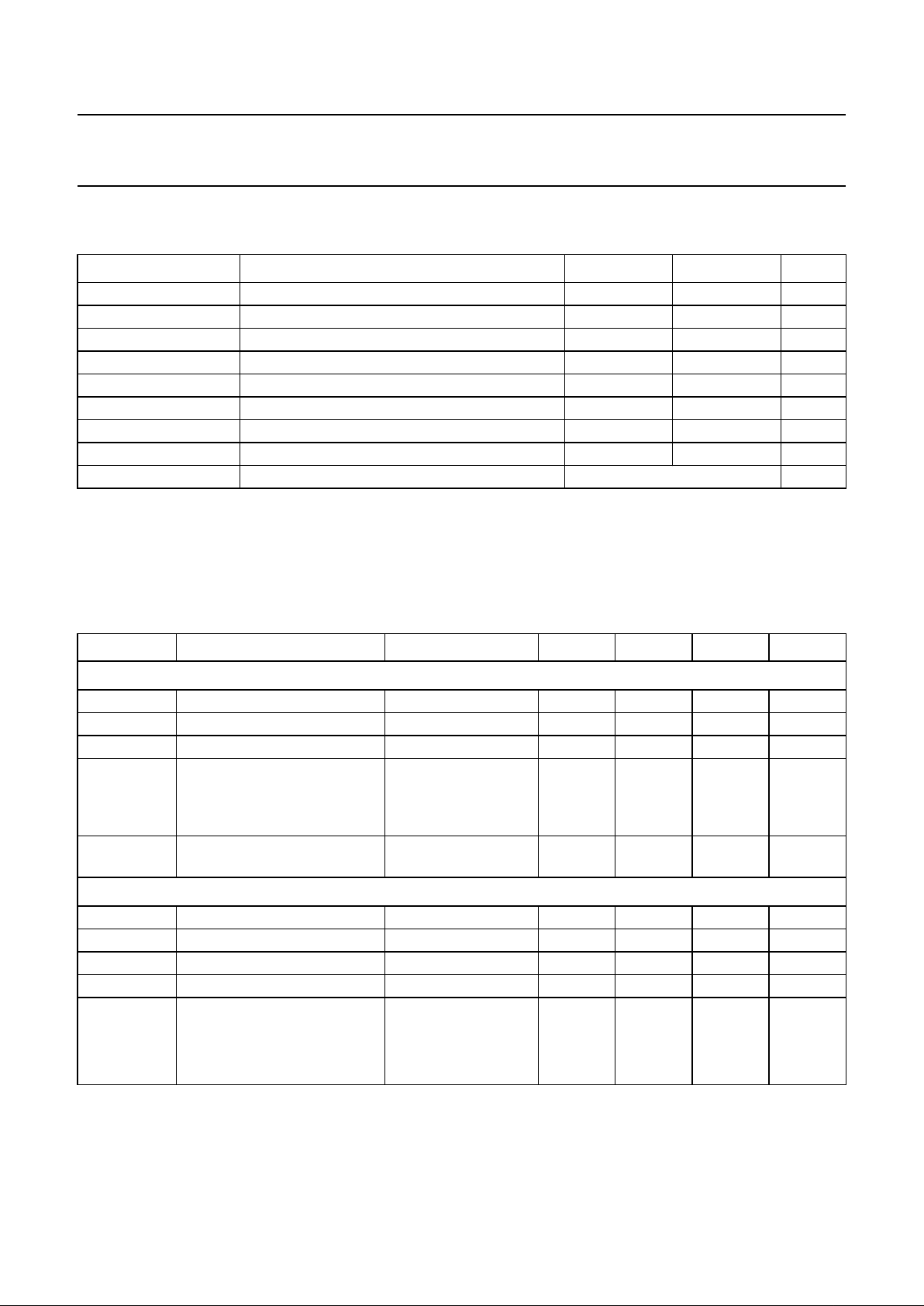
LIMITING VALUES
In accordance with Absolute Maximum System (IEC 134)
Note
1. Electrostatic handling Human body model: C = 100 pF, R = 1.5 kΩ and V ≥ 3 kV; charge device model:
C = 200 pF, R = 0 Ω and V ≥ 400 V.
DC CHARACTERISTICS
V
CC
= 12 V; T
amb
= 25 °C; unless otherwise specified
SYMBOL PARAMETER MIN. MAX. UNIT
V
CC
supply voltage 0 16 V
V
cap
voltage range for pins with external capacitors 0 V
CC
V
V
SDA, SCL
voltage range for pins 11 and 12 0 V
CC
V
V
I/O
voltage range at pins 1, 3, 9, 11, 12 and 13 0 V
CC
V
I
O
output current at pins 9 and 13 − 45 mA
P
tot
total power dissipation at T
amb
< 70 °C − 450 mW
T
amb
operating ambient temperature range 0 +70 °C
T
stg
storage temperature range −25 +150 °C
V
stat
electrostatic handling see note 1
SYMBOL PARAMETER CONDITIONS MIN. TYP. MAX. UNIT
Supplies
V
CC
supply voltage range 10.8 12.0 13.2 V
I
CC
supply current at VCC = 12 V − 26 35 mA
V
ref
internal reference voltage 5.4 0.5V
CC
6.6 V
V
I
internal voltage at pins 1 and 3 DC voltage internally
generated;
capacitive coupling
recommended
− V
ref
− V
V
O
internal voltage at pins 9 and
13
− V
ref
− V
SDA; SCL (pins 11 and 12)
V
IH
HIGH level input voltage 3.0 − V
CC
V
V
IL
LOW level input voltage −3.0 − 1.5 V
I
IH
HIGH level input current −−+10 µA
I
IL
LOW level input current −10 −−µA
output voltage at pins with
external capacitors
V
cap.n
pins 6 to 8, 14 to 16 − V
ref
− V
V
cap.2
pin 2 − VCC−0.3 − V
Page 11
September 1992 11
Philips Semiconductors Product specification
Hi-Fi stereo audio processor; I2C-bus
TDA8424
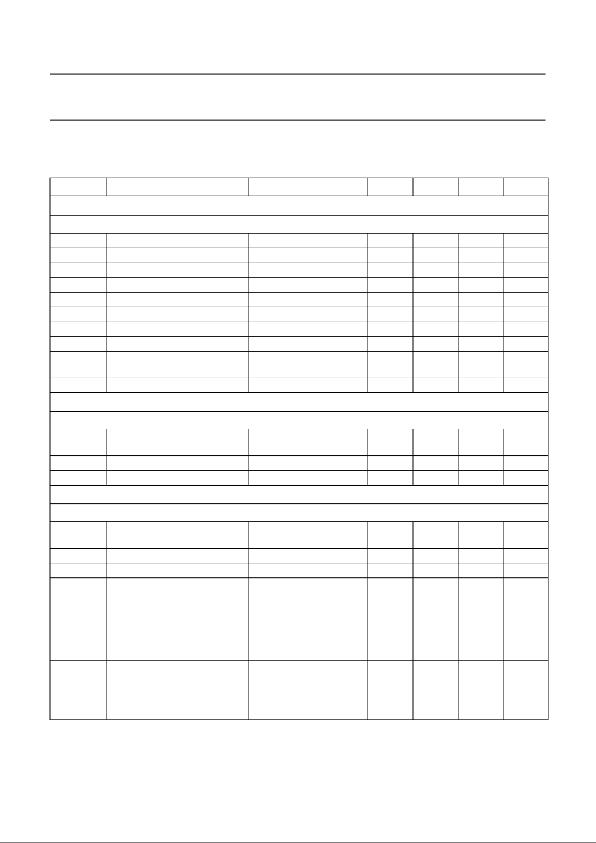
AC CHARACTERISTICS
V
CC
= 12 V; bass/treble in linear position; stereo mode; spatial stereo off; RL> 10 kΩ;CL<1000 pF; T
amb
=25°C;
unless otherwise specified
SYMBOL PARAMETER CONDITIONS MIN. TYP. MAX. UNIT
I
2
C-bus timing (see Fig.7)
SDA, SCL (PINS 11 AND 12)
f
SCL
clock frequency range 0 − 100 kHz
t
HIGH
clock HIGH period 4 −−µs
t
LOW
clock LOW period 4.7 −−µs
t
r
SCL rise time −−1µs
t
f
SCL fall time −−0.3 µs
t
SU;STA
set-up time for start condition 4.7 −−µs
t
HD;STA
hold time for start condition 4 −−µs
t
SU;STO
set-up time for stop condition 4.7 −−µs
t
BUF
time bus must be free before
a new transmission can start
4.7 −−µs
t
SU;DAT
data set-up time 250 −−ns
Inputs
INL(
PIN 1) IN R (PIN 3)
V
i(RMS)
input signal handling
(RMS value)
at Vu = −12 dB;
THD ≤ 0.5%
2 −−V
R
i
input resistance 20 30 40 kΩ
f frequency response (0.5 dB) 20 − 20 000 Hz
Outputs
OUTR(
PIN 9) OUT L (PIN 13)
V
o(RMS)
output voltage range
(RMS value)
at V
i(max)
≤ 2V;
THD ≤ 0.7%
0.6 −−V
R
L
load resistance 10 −−kΩ
Z
O
output impedance −−100 Ω
(S+N)/N signal plus noise-to-noise ratio weighted in accordance
with CCIR 468-2;
V
o
= 600 mV
gain = 6 dB − 78 − dB
gain = 0 dB − 86 − dB
gain ≤−20 dB − 68 − dB
THD total harmonic distortion f = 20 Hz to 12.5 kHz
gain = +6dBto−40 dB V
i(RMS)
= 0.3 V − 0.05 − %
gain = 0 dB to −40 dB V
i(RMS)
= 0.6 V − 0.07 0.4 %
gain = −12 dB to −40 dB V
i(RMS)
= 2.0 V − 0.1 − %
Page 12
September 1992 12
Philips Semiconductors Product specification
Hi-Fi stereo audio processor; I2C-bus
TDA8424
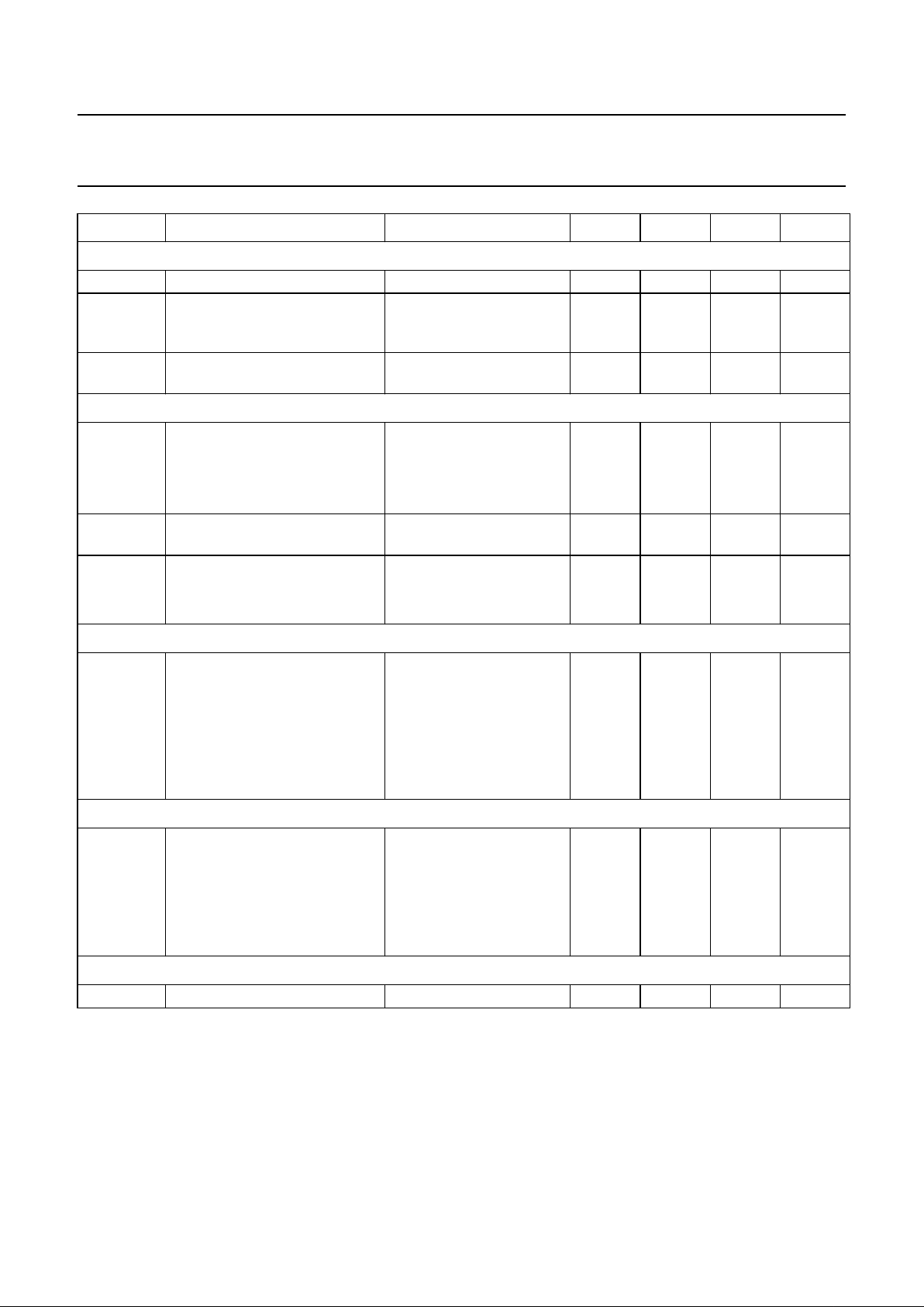
Note to the characteristics
1. Balance is obtained via software by different volume settings in both channels (left and right).
Outputs
α
cs
channel separation at 10 kHz gain = 0 dB − 80 − dB
RR
100
ripple rejection f
ripple
= 100 Hz;
V
r(RMS)
< 200 mV
gain = 0 dB
− 50 − dB
α
L
crosstalk attenuation from logic
inputs to AF outputs
gain = 0 dB − 100 − dB
Volume control (see Table 6)
control range (36 steps) f = 1 kHz
G
max
maximum voltage gain 6 dB step 5 6 − dB
G
min
minimum voltage gain −64 dB step −63 −64 − dB
G
mute
mute position −80 −90 − dB
G
err
gain tracking error;
balance in mid-position
−−2dB
G
step
step resolution
gain from +6dBto−40 dB 1.5 2.0 2.5 dB/step
gain from −42 dB to −64 dB 1.0 2.0 3.0 dB/step
Treble control (see Table 8)
G
emp
control range C
8-5
; C
14-5
= 5.6 nF
maximum emphasis at 15 kHz
with respect to linear position
11 12 13 dB
G
att
maximum attenuation at
15 kHz
with respect to linear position
11 12 13 dB
G
step
resolution 2.5 3.0 3.5 dB/step
Bass control (see Table 7)
G
emp
control range C
6-7
; C
15-16
= 33 nF
maximum emphasis at 40 Hz
with respect to linear position
14 15 16 dB
G
att
maximum attenuation at 40Hz
with respect to linear position
11 12 13 dB
G
step
resolution 2.5 3.0 3.5 dB/step
Spatial function
α antiphase crosstalk − 52 − %
SYMBOL PARAMETER CONDITIONS MIN. TYP. MAX. UNIT
Page 13
September 1992 13
Philips Semiconductors Product specification
Hi-Fi stereo audio processor; I2C-bus
TDA8424
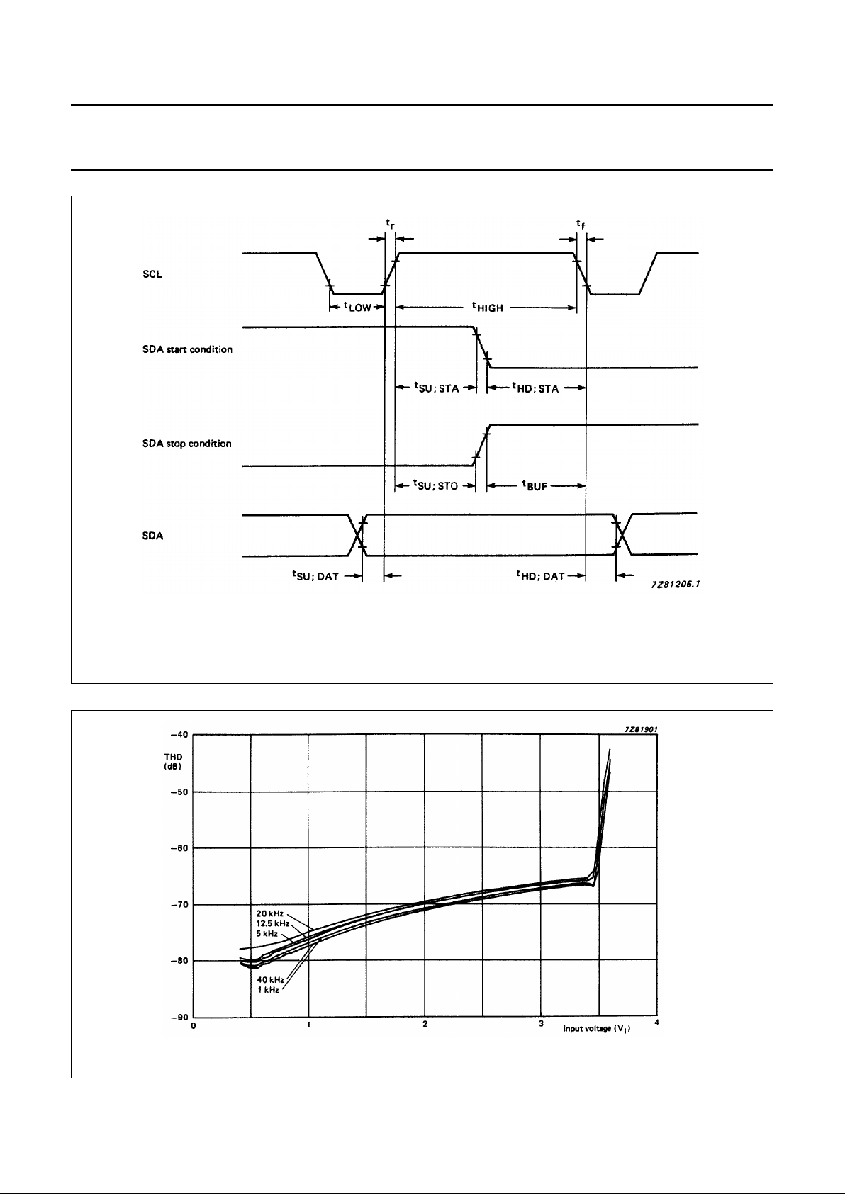
Fig.7 Timing requirements for I2C-bus.
t
SU; STA
= start code set-up time.
t
HD; STA
= start code hold time.
t
SU; STO
= stop code set-up time.
t
BUF
= bus free time.
t
SU; DAT
= data set-up time.
t
HD; DAT
= data hold time.
Fig.8 Input signal handling capability; gain = −10 dB; RS = 600 Ω;RL = 10 kΩ; bass/treble = 0 dB; VCC = 12 V.
Page 14
September 1992 14
Philips Semiconductors Product specification
Hi-Fi stereo audio processor; I2C-bus
TDA8424
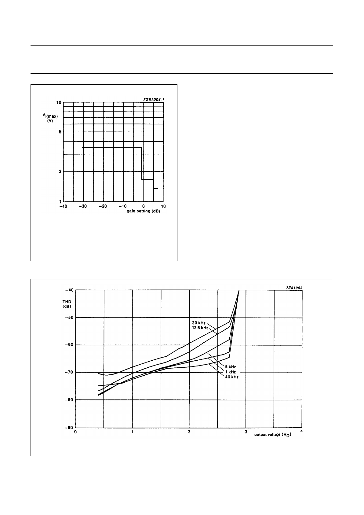
Fig.9 Input signal handling capability plotted
against gain setting; THD = −60 dB;
f = 1 kHz; RS= 600 Ω; RL=10kΩ;
bass/treble = 0 dB; VCC=12V.
Fig.10 Output signal handling capability; gain = 6 dB; RS = 600 Ω;RL = 10 kΩ; bass/treble = 0 dB; VCC = 12 V.
Page 15
September 1992 15
Philips Semiconductors Product specification
Hi-Fi stereo audio processor; I2C-bus
TDA8424
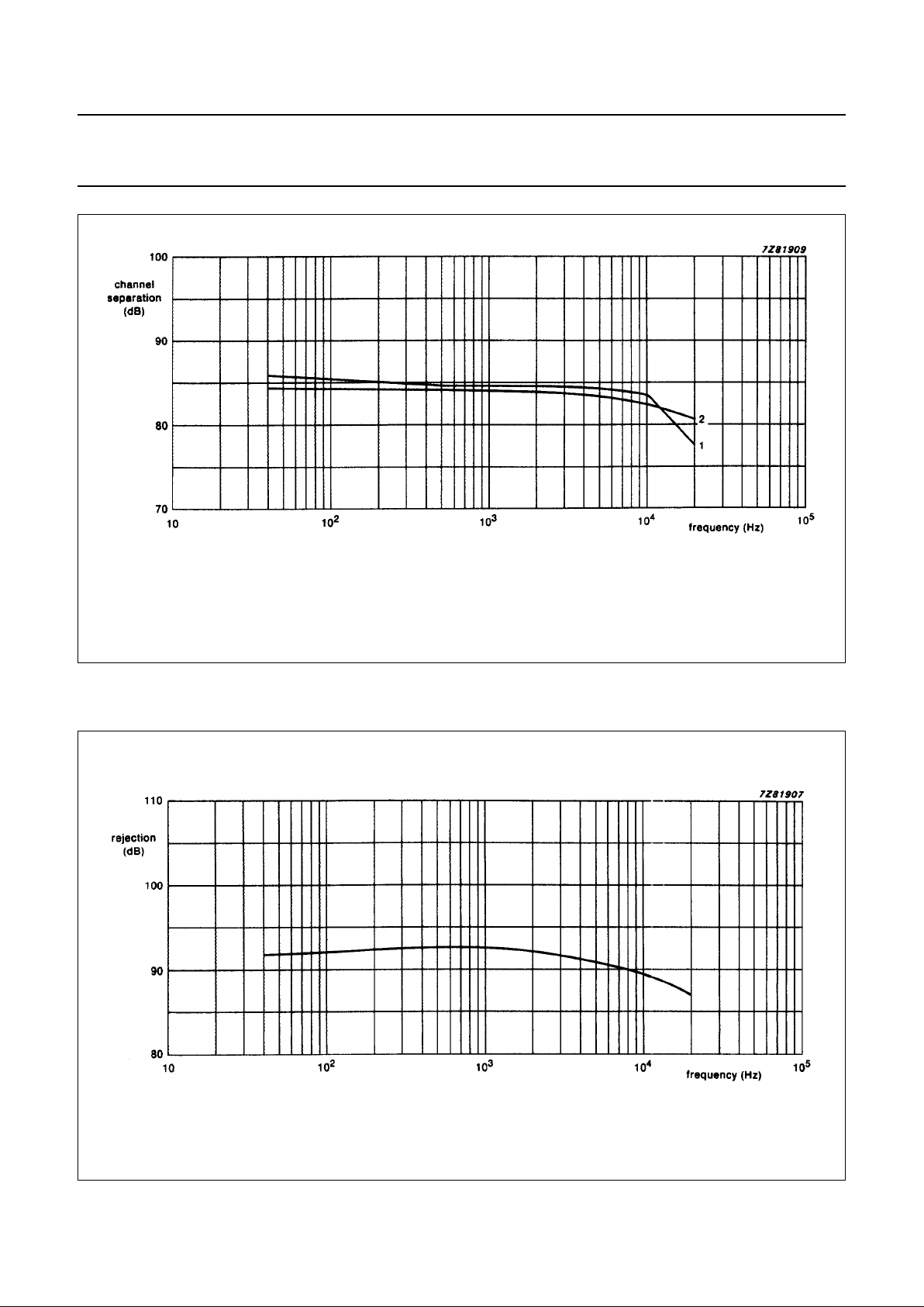
Fig.11 Stereo channel separation as a function of frequency; RS = 0 Ω;RL = 10 kΩ;
bass/treble = 0 dB; VCC = 12 V.
(1) gain = 0 dB; Vi= 1.0 V.
(2) gain = 6 dB; Vi= 0.5 V.
Fig.12 Mute signal rejection as a function of frequency; gain = 0 dB; Vi = 1.0 V; RS = 0 Ω;RL=10kΩ;
bass/treble = 0 dB; VCC = 12 V.
Page 16
September 1992 16
Philips Semiconductors Product specification
Hi-Fi stereo audio processor; I2C-bus
TDA8424
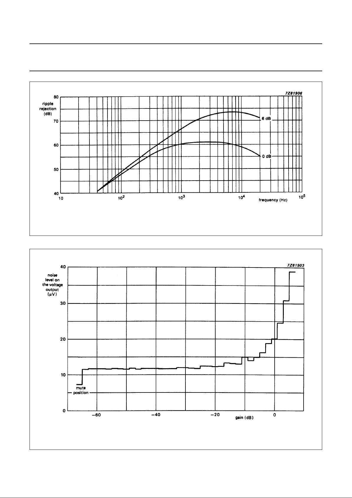
Fig.13 Ripple rejection as a function of frequency; V
ripple
= 0.3 V (RMS); RS = 0 Ω;RL =10kΩ;
bass/treble = 0 dB; VCC=12V.
Fig.14 Noise output voltage as a function of gain; weighted CCIR 468 quasi peak gain, +6dBto−64 dB;
Vi= 0 V; RS=0Ω;RL = 10 kΩ; bass/treble = 0 dB; VCC = 12 V.
Page 17
September 1992 17
Philips Semiconductors Product specification
Hi-Fi stereo audio processor; I2C-bus
TDA8424
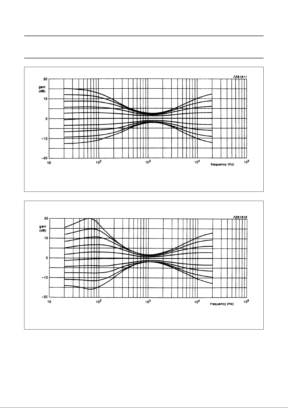
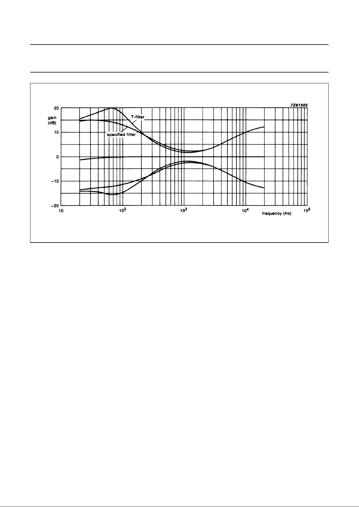
Fig.15 Frequency response of bass and treble control; bass and treble gain settings = −12 dB to +15 dB;
gain = 0 dB; Vi= 0.1 V; RS = 600 Ω;RL = 10 kΩ;VCC = 12 V.
Fig.16 Tone control with T-filter.
Page 18
September 1992 18
Philips Semiconductors Product specification
Hi-Fi stereo audio processor; I2C-bus
TDA8424
Fig.17 Tone control.
Page 19
September 1992 19
Philips Semiconductors Product specification
Hi-Fi stereo audio processor; I2C-bus
TDA8424
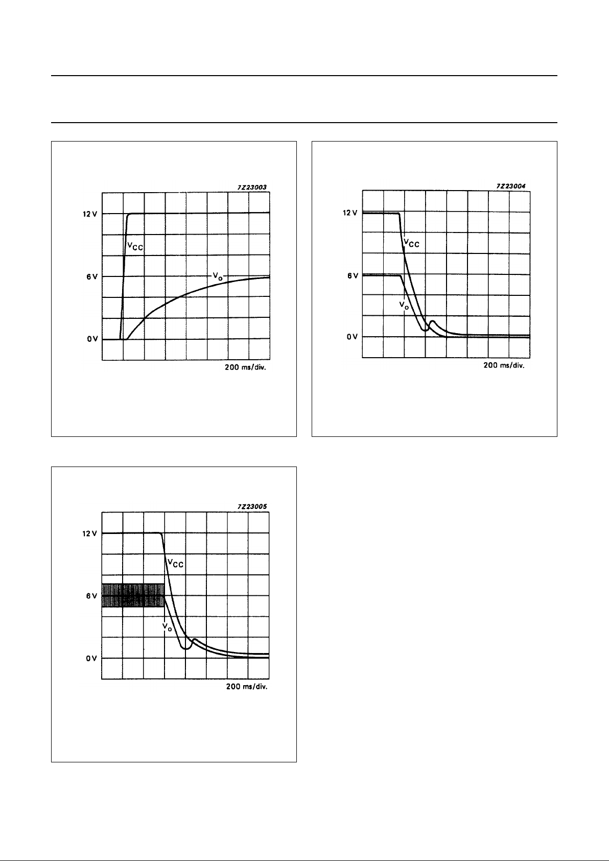
Fig.18 Turn-on behaviour; C = 2.2 µF; RL = 10 kΩ. Fig.19 Turn-off behaviour; without modulation.
Fig.20 Turn-off behaviour; with modulation
(shaded area).
Page 20
September 1992 20
Philips Semiconductors Product specification
Hi-Fi stereo audio processor; I2C-bus
TDA8424
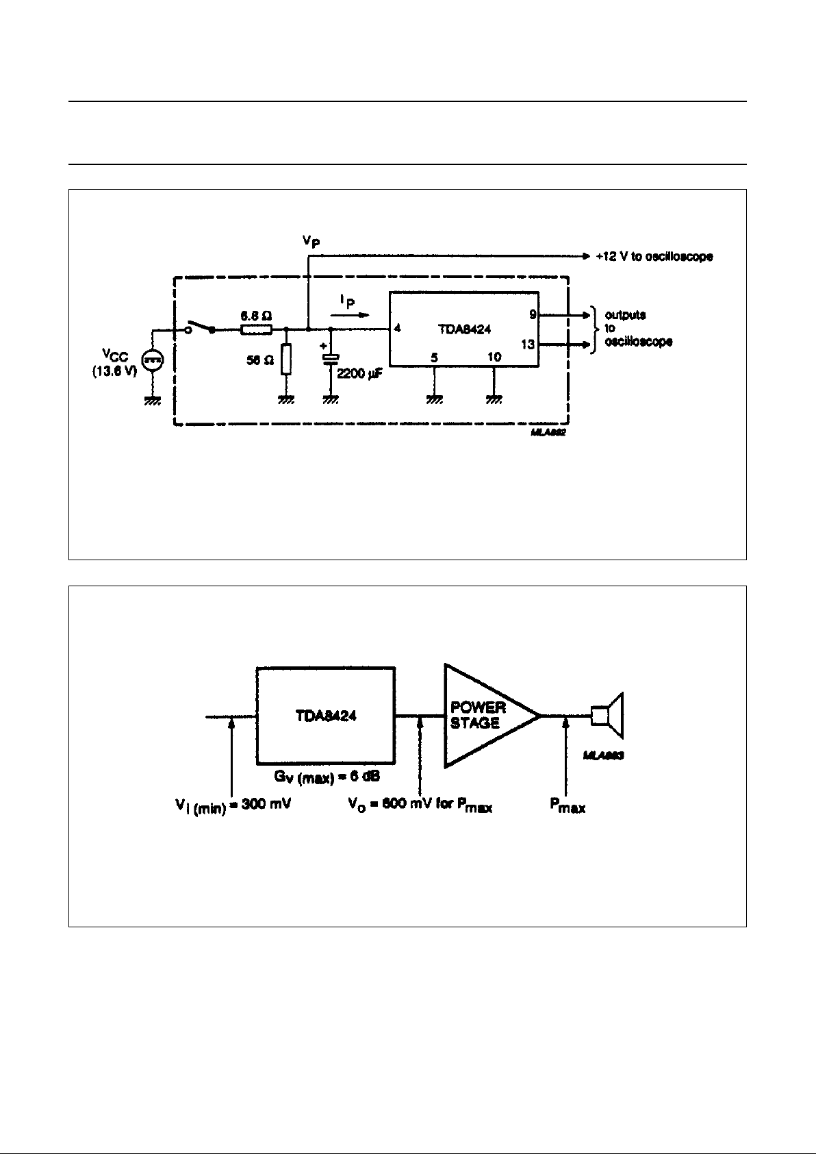
Fig.21 Turn-on/off power supply circuit diagram.
ICC = 25 mA
I
load
= 239 mA
ton = 15 ms
t
off
= 110 ms
Fig.22 Level diagram.
Page 21
September 1992 21
Philips Semiconductors Product specification
Hi-Fi stereo audio processor; I2C-bus
TDA8424
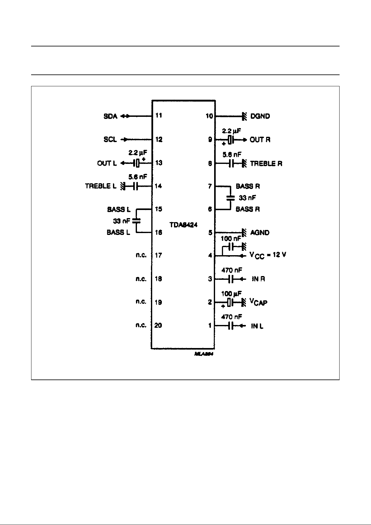
Fig.23 Test and application circuit diagram.
Page 22
September 1992 22
Philips Semiconductors Product specification
Hi-Fi stereo audio processor; I2C-bus
TDA8424
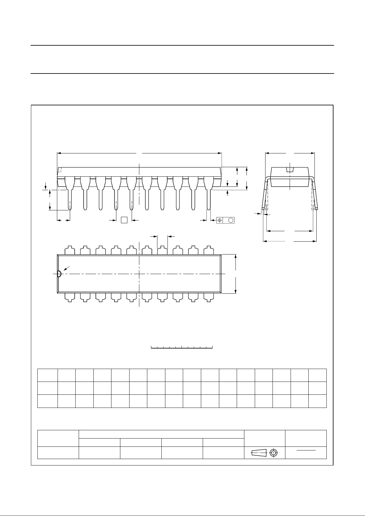
PACKAGE OUTLINE
UNIT
A
max.
1 2
b
1
cD E e M
H
L
REFERENCES
OUTLINE
VERSION
EUROPEAN
PROJECTION
ISSUE DATE
IEC JEDEC EIAJ
mm
inches
DIMENSIONS (inch dimensions are derived from the original mm dimensions)
SOT146-1
92-11-17
95-05-24
A
min.
A
max.
b
Z
max.
w
M
E
e
1
1.73
1.30
0.53
0.38
0.36
0.23
26.92
26.54
6.40
6.22
3.60
3.05
0.2542.54 7.62
8.25
7.80
10.0
8.3
2.04.2 0.51 3.2
0.068
0.051
0.021
0.015
0.014
0.009
1.060
1.045
0.25
0.24
0.14
0.12
0.010.10 0.30
0.32
0.31
0.39
0.33
0.0780.17 0.020 0.13
SC603
M
H
c
(e )
1
M
E
A
L
seating plane
A
1
w M
b
1
e
D
A
2
Z
20
1
11
10
b
E
pin 1 index
0 5 10 mm
scale
Note
1. Plastic or metal protrusions of 0.25 mm maximum per side are not included.
(1)
(1) (1)
DIP20: plastic dual in-line package; 20 leads (300 mil)
SOT146-1
Page 23
September 1992 23
Philips Semiconductors Product specification
Hi-Fi stereo audio processor; I2C-bus
TDA8424
SOLDERING
Introduction
There is no soldering method that is ideal for all IC
packages. Wave soldering is often preferred when
through-hole and surface mounted components are mixed
on one printed-circuit board. However, wave soldering is
not always suitable for surface mounted ICs, or for
printed-circuits with high population densities. In these
situations reflow soldering is often used.
This text gives a very brief insight to a complex technology.
A more in-depth account of soldering ICs can be found in
our
“IC Package Databook”
(order code 9398 652 90011).
Soldering by dipping or by wave
The maximum permissible temperature of the solder is
260 °C; solder at this temperature must not be in contact
with the joint for more than 5 seconds. The total contact
time of successive solder waves must not exceed
5 seconds.
The device may be mounted up to the seating plane, but
the temperature of the plastic body must not exceed the
specified maximum storage temperature (T
stg max
). If the
printed-circuit board has been pre-heated, forced cooling
may be necessary immediately after soldering to keep the
temperature within the permissible limit.
Repairing soldered joints
Apply a low voltage soldering iron (less than 24 V) to the
lead(s) of the package, below the seating plane or not
more than 2 mm above it. If the temperature of the
soldering iron bit is less than 300 °C it may remain in
contact for up to 10 seconds. If the bit temperature is
between 300 and 400 °C, contact may be up to 5 seconds.
DEFINITIONS
LIFE SUPPORT APPLICATIONS
These products are not designed for use in life support appliances, devices, or systems where malfunction of these
products can reasonably be expected to result in personal injury. Philips customers using or selling these products for
use in such applications do so at their own risk and agree to fully indemnify Philips for any damages resulting from such
improper use or sale.
PURCHASE OF PHILIPS I
2
C COMPONENTS
Data sheet status
Objective specification This data sheet contains target or goal specifications for product development.
Preliminary specification This data sheet contains preliminary data; supplementary data may be published later.
Product specification This data sheet contains final product specifications.
Limiting values
Limiting values given are in accordance with the Absolute Maximum Rating System (IEC 134). Stress above one or
more of the limiting values may cause permanent damage to the device. These are stress ratings only and operation
of the device at these or at any other conditions above those given in the Characteristics sections of the specification
is not implied. Exposure to limiting values for extended periods may affect device reliability.
Application information
Where application information is given, it is advisory and does not form part of the specification.
Purchase of Philips I
2
C components conveys a license under the Philips’ I2C patent to use the
components in the I2C system provided the system conforms to the I2C specification defined by
Philips. This specification can be ordered using the code 9398 393 40011.
 Loading...