

Page 1

INTEGRATED CIRCUITS
DATA SH EET
TDA8415
TV and VTR stereo/dual sound
processor with integrated filters and
2
I
C-bus control
Preliminary specification
File under Integrated Circuits, IC02
May 1989
Page 2
Philips Semiconductors Preliminary specification
TV and VTR stereo/dual sound processor with
integrated filters and I
GENERAL DESCRIPTION
The TDA8415 is a processor of stereo/dual language
signals (B/G-standard) for stereo sound television
receivers and VTRs, using the switched-capacitor
technique. The AF signals at the TDA8415 inputs must be
“(L+R)/2” or “language A” on one channel and “R” or
“language B” on the second channel (where L = left and
R = right). The carrier frequency of the second channel is
also modulated by an identification signal (stereo or dual
sound). The device is controlled by a microcomputer via
the two-line, bidirectional I2C-bus.
2
C-bus control
Features
• Use of the switched-capacitor technique for signal
processing
• Small amount of peripheral components
• Integrated anti-aliasing filters
• Low distortion AF signal handling
• Integrated de-emphasis with a time constant of 50 µs
• Function and software are compatible with the TDA8405
• Two general purpose output ports
• Full ESD protection
TDA8415
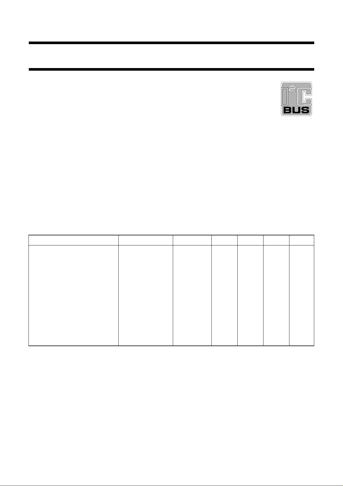
QUICK REFERENCE DATA
PARAMETER CONDITION SYMBOL MIN. TYP. MAX. UNIT
Supply voltage (pin 15) V
Supply current (pin 15) I
AF output signal (RMS value)
(pins 11 to 14) V
Weighted signal-to-noise
ratio of the AF output
signals (CCIR 468/3)
Crosstalk attenuation
stereo mode at f = 1 kHz α
dual sound mode at f = 40 Hz to 12.5 kHz α
Pilot signal input sensitivity V
Total harmonic distortion THD − 0.1 − %
PACKAGE OUTLINE
20-lead DIL; plastic (SOT146);SOT146-1; 1996 December 18.
P
P
o
(S+W)/W 70 −−dB
S
DS
i
− 12 − V
− 10 − mA
− 2 − V
40 −−dB
70 −−dB
− 2.5 − mV
May 1989 2
Page 3

Philips Semiconductors Preliminary specification
TV and VTR stereo/dual sound processor
with integrated filters and I
2
C-bus control
TDA8415
May 1989 3
Fig.1 Block diagram.
Page 4

Philips Semiconductors Preliminary specification
TV and VTR stereo/dual sound processor
with integrated filters and I
2
C-bus control
TDA8415
Fig.2 Input and output loading diagram.
May 1989 4
Page 5

Philips Semiconductors Preliminary specification
TV and VTR stereo/dual sound processor
TDA8415
2
C-bus)
2
C-bus)
2
C-bus control
11 Output A4 AF 2 output
12 Output A3 AF 2 output
13 Output A2 AF 1 output
13 Output A1 AF 1 output
15 Supply voltage V
16 Analogue ground (0 V)
17 Ripple rejection improvement
18 Mute input
19 Control port C2
20 Not connected, but reserved
P
with integrated filters and I
PINNING
1 Control port C1
2 SDA, serial data line (I
3 SCL, serial clock line (I
4 Oscillator input (or quartz)
5 Digital ground (0 V)
6 Not connected, but reserved
7 Sound channel input AF2 (E2)
8 Sound channel input AF1 (E1)
9 External AF input (E4)
10 External AF input (E3)
FUNCTIONAL DESCRIPTION
Anti-aliasing filters
Frequency band limitation is performed by a second order Sallen and Key low-pass filter inserted in the AF signal path
and the identification circuit. This limitation is necessary because of the time-discrete signal processing needed to meet
the Nyquist criterion.
Identification
To enable the identification of the transmitted AF signal (mono, stereo or dual sound), the carrier frequency of the second
channel (E2) is also modulated by an identification signal. The identification signal is a 54.6875 kHz pilot carrier signal
which is 50% amplitude modulated by either a 117.4 Hz signal for stereo transmission or by a 274.1 Hz signal for dual
sound transmission.
The identification section of the circuit consists of a 54 kHz high-pass filter followed by a gain controlled amplifier with an
AM demodulator. The total gain of the high-pass filter and the amplifier is approximately 56 dB. The demodulated
identification signal is filtered by the identification band-pass filters, (117.4 Hz for stereo transmission, 274.1 Hz for dual
sound transmission). The output from either filter is converted to a DC signal by a peak detector and the necessary
hysteresis is performed by a Schmitt-trigger. The resultant DC output signals indicate the status of the transmitter (mono,
stereo or dual sound).
De-matrix and de-emphasis
Depending on the results of the identification circuit (mono, stereo or dual sound) the AF signals at the inputs E1 and E2
are converted to the signals at E1* and E2* as listed in Table 1.
Table 1 Transmitter status
TRANSMITTER STATUS
mono 0.7(L+R) − 2(L+R) −
stereo 0.7(L+R) 2R 4L 4R
dual sound 0.7A B 2A 2B
(1)
E1 E2 E1* E2*
Note
1. Where L = left channel signal; R = right channel signal; A = first sound channel signal and B = second sound channel
signal.
This section of the circuit also performs the de-emphasis (50 µs time constant) with a high degree of accuracy.
May 1989 5
Page 6

Philips Semiconductors Preliminary specification
TV and VTR stereo/dual sound processor
with integrated filters and I
AF switch
The AF switch is used to switch to either the internal sound sources (E1* or E1* and E2*) or, to the external sound source
(E3 and E4) and is controlled via the I2C-bus.
Source selector
The source selector is used to connect the outputs from the AF switch to the outputs A1 to A4 as illustrated by Table 5.
The selector is controlled via the I
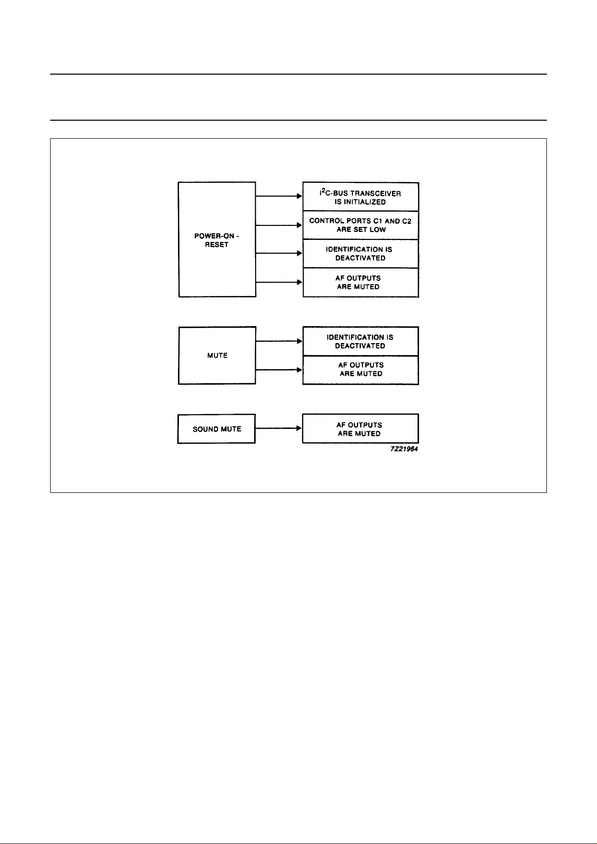
Muting
In this mode the AF outputs A1 to A4 are muted, and the identification circuit is deactivated (mono). The muting is active
after power-on reset or as a result of user control (via the mute input and bit CR3 of the control byte of the mute and port
control register; see Table 4).
Sound mute
If the switch register is set to (00) hex, (sound mute) only the AF outputs are muted, the identification circuit is still active
and can be read (status register) via the I
Power-on reset
2
C-bus.
2
C-bus control
2
C-bus.
TDA8415
The following actions are carried out by the internal power-on reset when it is active:
• The AF outputs are muted
• The identification circuit is deactivated (mono)
• The control ports (C1 and C2) are set LOW
2
• The I
When the power-on reset becomes passive the following occurs:
• The AF outputs are kept in the mute state until the contents of the switch register are changed from (00) hex via the
• The identification circuit is activated
• The control ports are LOW until the mute and control port register is changed (CR bits 10, 11, 20 and 21)
• The I2C-bus transceiver is activated
C-bus transceiver is initialized
I2C-bus
May 1989 6
Page 7
Philips Semiconductors Preliminary specification
TV and VTR stereo/dual sound processor
with integrated filters and I
2
C-bus control
TDA8415
Fig.3 Mute modes.
May 1989 7
Page 8
Philips Semiconductors Preliminary specification
TV and VTR stereo/dual sound processor
with integrated filters and I
Control ports
The general purpose control ports C1 and C2 can be set to LOW, HIGH or high impedance via the I2C-bus.
2
C-bus receiver and data handling
I
Bus specification
The TDA8415 is controlled, via the bidirectional 2-line I2C-bus, by a microcomputer. The two lines are a serial data line
(SDA) and a serial clock line (SCL). Both lines must be connected to a positive supply via a pull-up resistor. Data transfer
may be initiated only when the bus is not busy.
When the bus is free both lines are HIGH. The data on the SDA line must be stable during the HIGH period of the clock.
The HIGH or LOW state of the data line can only change when the clock signal on the SCL line is LOW. The set up and
hold times are specified in the CHARACTERISTICS.
A HIGH-to-LOW transition of the SDA line while SCL is HIGH is defined as the start condition (S). A LOW-to-HIGH
transition of the SDA line while SCL is HIGH is defined as the stop condition (P). The bus receiver will be reset on the
reception of a start condition. The bus is considered to be busy after the start condition. The bus is considered to be free
again after a stop condition.
2
C-BUS PROTOCOL OF THE TDA8415
The I
2
C-bus control
TDA8415
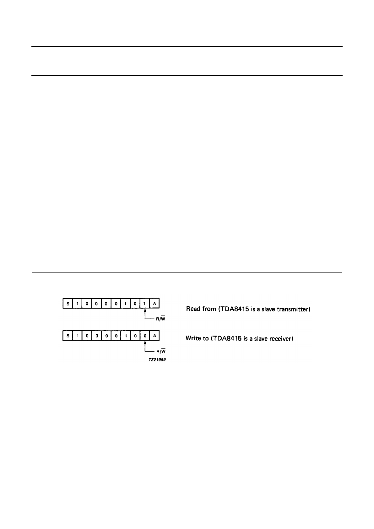
The TDA8415 is controlled by a microcomputer and can be written to or read from via the I2C-bus.
The first byte is the address and determines whether the TDA8415 is to be read from (status register) or written to (switch
register or mute and port control register).
Where S = start bit and A = acknowledge bit
Fig.4 Address byte.
May 1989 8
Page 9
Philips Semiconductors Preliminary specification
TV and VTR stereo/dual sound processor
with integrated filters and I
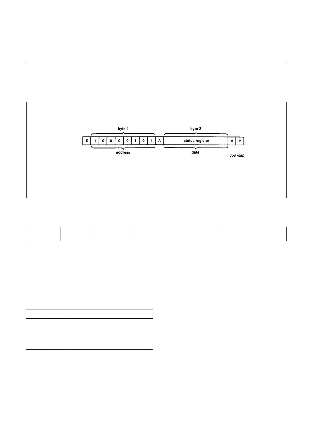
Reading the TDA8415
Reading the TDA8415 means reading the status register and the data stream will have the format as illustrated in Fig.5
below.
Where S = start bit; A = acknowledge bit and P = stop bit
2
C-bus control
Fig.5 Read format.
TDA8415
The second byte, the contents of the status register, is defined by Table 2.
Table 2 Status register
D7
PONRES
PONRES = power on reset
1 = power on reset active after switching on or power breakdown
0 = after reading the status register
ST = stereo transmission
DS = dual sound transmission
The truth table for the ST and DS bits is provided by Table 3.
Table 3 Truth table for ST and DS bits
ST DS definition
0 0 mono transmission
0 1 dual sound transmission
1 0 stereo transmission
1 1 not possible
D6
ST
D5
DS
D4
0
D3
0
D2
0
D1
0
D0
0
May 1989 9
Page 10
Philips Semiconductors Preliminary specification
TV and VTR stereo/dual sound processor
with integrated filters and I
Writing to the TDA8415
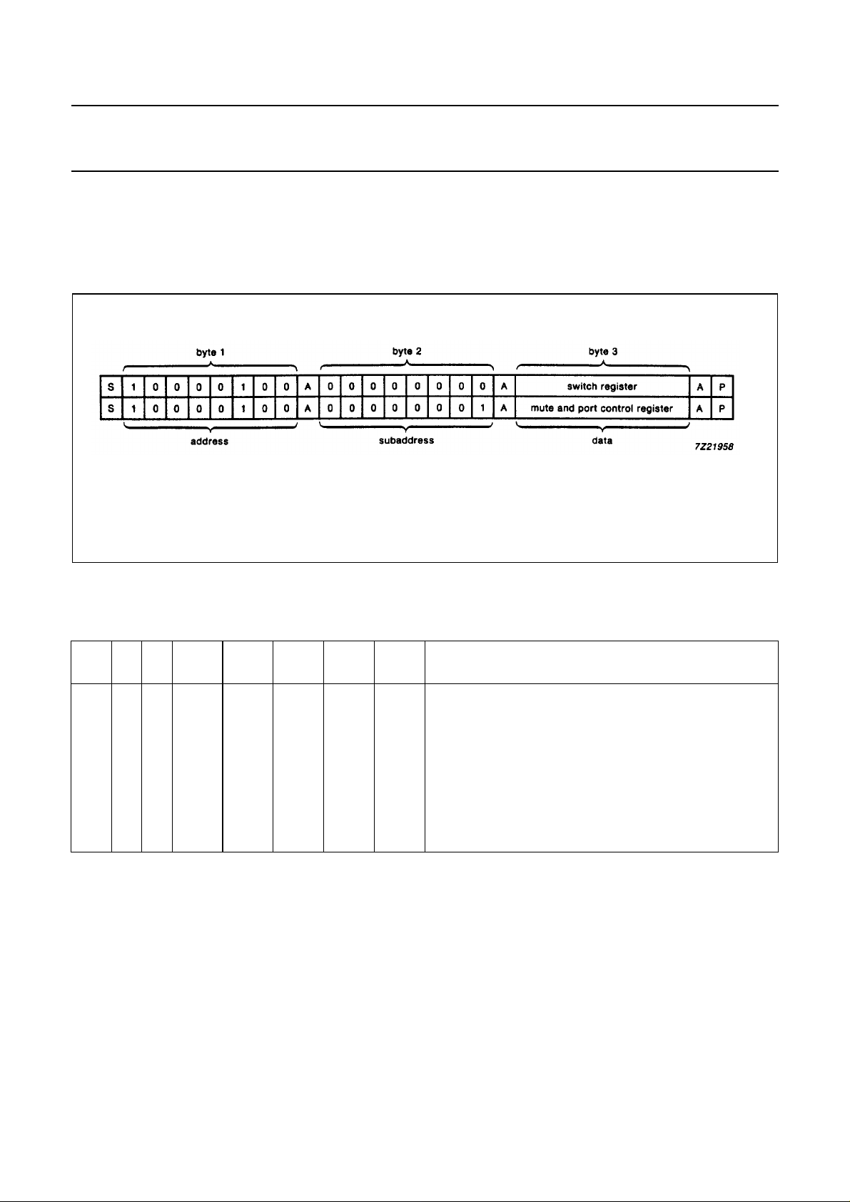
Writing to the TDA8415 means, writing to either the switch register or the mute and port control register. Which one is to
be addressed is defined by the subaddress (the second byte) as illustrated by Fig.6 below. The third byte contains the
information to be stored in the specified register.
Where S = start bit; A = acknowledge bit and P = stop bit
2
C-bus control
Fig.6 Write format.
TDA8415
Table 4 defines the contents of the mute and port control register.
Table 4 Mute and port control register
D7 D6 D5
X X X 0 0 control port C1 = LOW
X X X 0 1 control port C1 = HIGH
X X X 1 X control port C1 = high impedance
X X X 0 0 control port C2 = LOW
X X X 0 1 control port C2 = HIGH
X X X 1 X control port C2 = high impedance
X X X 0 mute is active when pin 18 is LOW (default)
X X X 1 mute is active when pin 18 is HIGH
Note
1. Where: X = don’t care.
D4
CR3D3CR21D2CR20D1CR11D0CR10
definition
May 1989 10
Page 11

Philips Semiconductors Preliminary specification
TV and VTR stereo/dual sound processor
with integrated filters and I
Table 5 defines the contents of the switch register.
Table 5 Switch register
SWITCH
REGISTER
sound mute −−−−−no signal 0 0 0 0 0 0 0 0 (00)
mono M M M −−M M M M 0 0 0 1 0 0 0 0 (10)
stereo St L* R −−L R L R 0 0 1 0 1 0 1 0 (2A)
sound A DS A B −−A A A A 0 0 0 1 0 0 0 0 (10)
sound B DS A B −−B B B B 0 0 0 1 1 1 1 1 (1F)
dual sound DS A B −−A A B B 0 0 0 1 1 1 0 0 (1C)
INPUT OUTPUT D7 D6 D5 D4 D3 D2 D1 D0 (HEX)
E1 E2 E3 E4 A1 A2 A3 A4
St L* R −−L* L* L* L* 0 0 0 1 0 0 0 0 (10)
DS A B −−B B A A 0 0 0 1 0 0 1 1 (13)
2
C-bus control
TDA8415
dual sound DS A B −−A B A A 0 0 0 1 0 0 1 0 (12)
mix DS A B −−A A A B 0 0 0 1 1 0 0 0 (18)
DS A B −−A B A B 0 0 0 1 1 0 1 0 (1A)
DS A B −−B B A B 0 0 0 1 1 0 1 1 (1B)
DS A B −−A B B B 0 0 0 1 1 1 1 0 (1E)
external −− − E3 E4 E3 E3 E3 E3 0 1 1 1 0 0 0 0 (70)
−− − E3 E4 E4 E4 E4 E4 0 1 1 1 1 1 1 1 (7F)
−− − E3 E4 E3 E4 E3 E4 0 1 1 1 1 0 1 0 (7A)
−− − E3 E4 E4 E4 E3 E3 0 1 1 1 0 0 1 1 (73)
−− − E3 E4 E3 E3 E4 E4 0 1 1 1 1 1 0 0 (7C)
−− − E3 E4 E3 E4 E3 E3 0 1 1 1 0 0 1 0 (72)
−− − E3 E4 E3 E3 E3 E4 0 1 1 1 1 0 0 0 (78)
−− − E3 E4 E4 E4 E3 E4 0 1 1 1 1 0 1 1 (7B)
−− − E3 E4 E3 E4 E4 E4 0 1 1 1 1 1 1 0 (7E)
Note
1. Where: M = mono; St = stereo. DS = dual sound; R = right; L = left; L * = (L+R)/2; A = sound A; B = sound B.
May 1989 11
Page 12

Philips Semiconductors Preliminary specification
TV and VTR stereo/dual sound processor
with integrated filters and I
2
C-bus control
RATINGS
Limiting values in accordance with Absolute Maximum System (IEC 134)
PARAMETER SYMBOL MIN. TYP. MAX. UNIT
Supply voltage
(1)
VP=V
15-16
−−13.2 V
Output current
pins 11, 12, 13, 14 I
pins 1 and 19 (sink) I
(source) −I
Input voltage (not pin 18) V
Input voltage pin 18 V
Output voltage V
Total power dissipation P
O
O
O
I
I=V18-16
O
tot
−−10 mA
−−7mA
−−3mA
0 − V
−−7V
0 − V
−−1W
ESD protection (each pin) (0 Ω/200 pF) 500 −−V
Operating ambient temperature range T
Storage temperature range T
amb
stg
0 − +70 °C
−40 − +150 °C
Note
1. Supply voltage may be applied only when both pins 5 and 15 are connected to ground.
TDA8415
P
P
V
V
May 1989 12
Page 13

Philips Semiconductors Preliminary specification
TV and VTR stereo/dual sound processor
with integrated filters and I
2
C-bus control
CHARACTERISTICS
= 12 V; T
V
P
=25°C. Measurement conditions (see Fig.7): reference level is 1 V (RMS); test frequency = 3.183 kHz;
amb
noise measurement in accordance with DIN 45405, CCIR 468-3; oscillator frequency = 10 MHz; pre-emphasis time
constant = 50 µs.
PARAMETER CONDITIONS SYMBOL MIN. TYP. MAX. UNIT
Supplies
Supply voltage V
Supply current I
P=V15-16
P=I15
10.8 12 13.2 V
− 10 − mA
DC levels
pins 7 - 14 and 17 V
pin 4 V
n-16
4-5
− 3.25 − V
− 2 − V
Bus transceiver
Clock frequency
2
C-bus) note 1 f
(I
CLK
0.7 − 100 kHz
CLOCK SCL (PIN 3)
Input voltage LOW V
Input voltage HIGH V
Timing LOW period t
Timing HIGH period t
Rise time t
Fall time t
Input current LOW −I
Input current HIGH I
IL
IH
LOW
HIGH
r
f
IL
IH
−0.3 − 1.5 V
3 − 5V
4.7 −−µs
4 −−µs
−− 1µs
−− 0.3 µs
−− 10 µA
−− 10 µA
DATA SDA (PIN 2)
Input voltage LOW V
Input voltage HIGH V
Rise time t
Fall time t
Data set-up time t
Input current LOW −I
Input current HIGH I
Output current LOW I
IL
IH
r
f
SU; DAT
IL
IH
OL
−0.3 − 1.5 V
3 − 5V
−− 1µs
−− 0.3 µs
0.25 −−µs
−− 10 µA
−− 10 µA
3 −−mA
Mute port (pin 18)
Input voltage LOW note 2 V
Input voltage HIGH note 2 V
IL
IH
−0.3 − 1.5 V
3 − 5V
TDA8415
May 1989 13
Page 14

Philips Semiconductors Preliminary specification
TV and VTR stereo/dual sound processor
with integrated filters and I
2
C-bus control
PARAMETER CONDITIONS SYMBOL MIN. TYP. MAX. UNIT
Control ports
(pins 1 and 19)
Output voltage LOW note 3 V
Output voltage HIGH note 3 V
Output impedance 3-state Z
Output current LOW I
Output current HIGH −I
OL
OH
o
OL
OH
−− 0.5 V
4.5 − 5V
1 −−MΩ
1 −−mA
1 −−mA
AF stages and identification
(pins 7 to 14)
Input impedance
(pins 7 to 10) Z
Input voltage E1 V
Input voltage E2 V
i
I
I
150 200 − kΩ
−− 0.7 V
−− 1V
Input voltage E2 for
identification
note 4 V
i
2.5 −−mV
active (RMS value)
Voltage gain 7-15/output note 5 G
Voltage gain 8-15/output note 5 G
v
v
5.9 6 6.1 dB
8.9 9 9.1 dB
Voltage gain
9, 10−15/output G
v
−0.1 0 0.1 dB
Crosstalk attenuation notes 6 to 8
dual mode α
stereo mode α
ds
s
70 75 − dB
30 50 − dB
Output impedance
(pins 11 to 14) Z
o
400 500 600 Ω
De-emphasis time
constant note 9 49.5 50 50.5 µs
Frequency response note 6 ∆f −1 − 1dB
Total harmonic
distortion note 10 THD −− 0.2 %
Capacitive load
(pins 11 to 14) C
L
−− 1.5 nF
Output signal
(RMS value)
THD ≤ 0.2% V
o
−− 2V
(pins 11 to 14)
Ripple rejection note 11 RR 50 66 − dB
Noise from I2C-bus NR −− −80 dB
Signal-to-noise ratio (S+W)/W 70 −−dBV
TDA8415
CCIR
May 1989 14
Page 15

Philips Semiconductors Preliminary specification
TV and VTR stereo/dual sound processor
with integrated filters and I
PARAMETER CONDITIONS SYMBOL MIN. TYP. MAX. UNIT
AF stages and identification
(continued)
Signal suppression
during mute note 6 SS 70 75 − dB
Change of output
DC voltages level
between any two
modes
Oscillator
Oscillator frequency f
External oscillator
signal (RMS value) V
Quartz series resistor R1 −− 100 Ω
Impedance Z
Capacitance C
Notes to the characteristics
1. Full specification of I2C−bus will be supplied on request.
2. Programmable mute state. If the CR3 bit of the mute and port control register is LOW, the mute is active LOW; if it
is HIGH, the mute input is active HIGH.
3. Output current IO≈ 1 mA.
4. Unmodulated.
5. f = 400 Hz; RL=1 MΩ.
6. 40 Hz ≤ f ≤ 15 kHz.
7. In dual mode: A(B)-signal into B(A)-channel.
In stereo mode: R-signal into left, L-signal = 0, reference is 1 V RMS.
8. Source impedance |ZS| < 1 kΩ.
9. Equivalent to an output level of −3 dB at f = 3.183 kHz.
10. Vo= 1 V RMS; f = 1 kHz.
11. Test circuit see Fig.7.
2
C-bus control
OSC
4-5
i
OSC
−− 30 mV
− 10 − MHz
1.7 −−V
−−1.2 + j9.3 − kΩ
− 1.7 − pF
TDA8415
May 1989 15
Page 16
Philips Semiconductors Preliminary specification
TV and VTR stereo/dual sound processor
with integrated filters and I
2
C-bus control
TDA8415
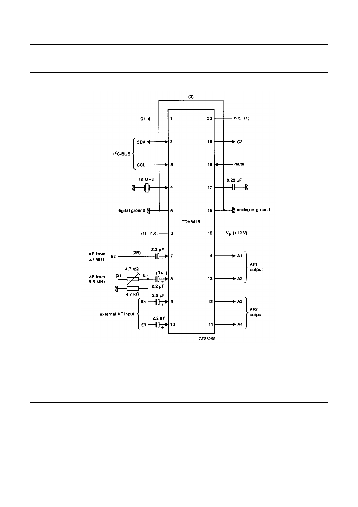
(1) These pins are not connected internally and should not be connected on the printed circuit board in order to maintain compatibility
with future devices.
(2) This potentiometer has to be adjusted to achieve the best stereo separation.
(3) Direct connection between pins 5 and 16 is needed.
Fig.7 Application and test circuit.
May 1989 16
Page 17
Philips Semiconductors Preliminary specification
TV and VTR stereo/dual sound processor
with integrated filters and I
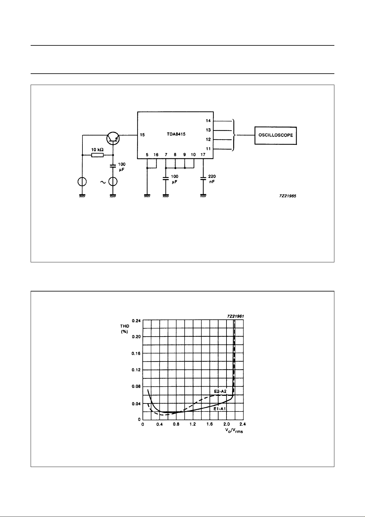
Voltage input = supply voltage + pulse voltage at 70 Hz = 12 V± 50 mV (p-p).
2
C-bus control
TDA8415
Fig.8 Ripple rejection test circuit.
Fig.9 Total harmonic distortion diagram (stereo mode).
May 1989 17
Page 18
Philips Semiconductors Preliminary specification
TV and VTR stereo/dual sound processor
with integrated filters and I
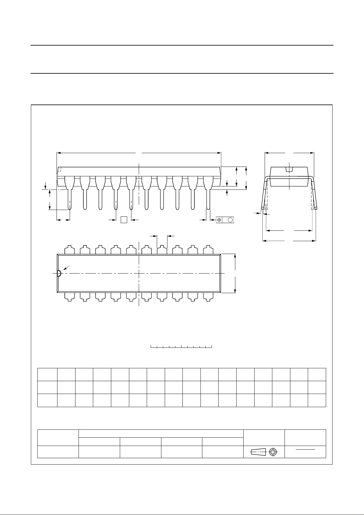
PACKAGE OUTLINE
DIP20: plastic dual in-line package; 20 leads (300 mil)
seating plane
L
Z
20
2
C-bus control
D
e
b
TDA8415
SOT146-1
M
E
A
2
A
A
1
w M
b
1
11
c
(e )
1
M
H
pin 1 index
1
0 5 10 mm
scale
DIMENSIONS (inch dimensions are derived from the original mm dimensions)
A
A
A
UNIT
inches
Note
1. Plastic or metal protrusions of 0.25 mm maximum per side are not included.
max.
mm
OUTLINE
VERSION
SOT146-1
1 2
min.
max.
1.73
1.30
0.068
0.051
IEC JEDEC EIAJ
b
b
1
0.53
0.38
0.021
0.015
0.36
0.23
0.014
0.009
REFERENCES
cD E e M
(1) (1)
26.92
26.54
1.060
1.045
SC603
6.40
6.22
0.25
0.24
E
10
(1)
M
e
L
1
3.60
8.25
3.05
7.80
0.14
0.32
0.12
0.31
EUROPEAN
PROJECTION
H
E
10.0
0.2542.54 7.62
8.3
0.39
0.010.10 0.30
0.33
ISSUE DATE
w
92-11-17
95-05-24
Z
max.
2.04.2 0.51 3.2
0.0780.17 0.020 0.13
May 1989 18
Page 19
Philips Semiconductors Preliminary specification
TV and VTR stereo/dual sound processor
with integrated filters and I
SOLDERING
Introduction
There is no soldering method that is ideal for all IC
packages. Wave soldering is often preferred when
through-hole and surface mounted components are mixed
on one printed-circuit board. However, wave soldering is
not always suitable for surface mounted ICs, or for
printed-circuits with high population densities. In these
situations reflow soldering is often used.
This text gives a very brief insight to a complex technology.
A more in-depth account of soldering ICs can be found in
“IC Package Databook”
our
Soldering by dipping or by wave
The maximum permissible temperature of the solder is
260 °C; solder at this temperature must not be in contact
DEFINITIONS
(order code 9398 652 90011).
2
C-bus control
TDA8415
with the joint for more than 5 seconds. The total contact
time of successive solder waves must not exceed
5 seconds.
The device may be mounted up to the seating plane, but
the temperature of the plastic body must not exceed the
specified maximum storage temperature (T
printed-circuit board has been pre-heated, forced cooling
may be necessary immediately after soldering to keep the
temperature within the permissible limit.
Repairing soldered joints
Apply a low voltage soldering iron (less than 24 V) to the
lead(s) of the package, below the seating plane or not
more than 2 mm above it. If the temperature of the
soldering iron bit is less than 300 °C it may remain in
contact for up to 10 seconds. If the bit temperature is
between 300 and 400 °C, contact may be up to 5 seconds.
stg max
). If the
Data sheet status
Objective specification This data sheet contains target or goal specifications for product development.
Preliminary specification This data sheet contains preliminary data; supplementary data may be published later.
Product specification This data sheet contains final product specifications.
Limiting values
Limiting values given are in accordance with the Absolute Maximum Rating System (IEC 134). Stress above one or
more of the limiting values may cause permanent damage to the device. These are stress ratings only and operation
of the device at these or at any other conditions above those given in the Characteristics sections of the specification
is not implied. Exposure to limiting values for extended periods may affect device reliability.
Application information
Where application information is given, it is advisory and does not form part of the specification.
LIFE SUPPORT APPLICATIONS
These products are not designed for use in life support appliances, devices, or systems where malfunction of these
products can reasonably be expected to result in personal injury. Philips customers using or selling these products for
use in such applications do so at their own risk and agree to fully indemnify Philips for any damages resulting from such
improper use or sale.
2
PURCHASE OF PHILIPS I
C COMPONENTS
Purchase of Philips I
components in the I2C system provided the system conforms to the I2C specification defined by
Philips. This specification can be ordered using the code 9398 393 40011.
May 1989 19
2
C components conveys a license under the Philips’ I2C patent to use the
 Loading...