

Page 1

INTEGRATED CIRCUITS
DATA SH EET
TDA8366
2
I
C-bus controlled PAL/NTSC TV
processor
Objective specification
File under Integrated Circuits, IC02
Philips Semiconductors
January 1995
Page 2

Philips Semiconductors Objective specification
I2C-bus controlled PAL/NTSC TV
processor
FEATURES
• Multistandard vision IF circuit (positive and
negative modulation)
• Video identification circuit in the IF circuit which is
independent of the synchronization for stable On Screen
Display (OSD) under ‘no-signal’ conditions
• Source selection with 2 Colour Video Blanking
Synchronization (CVBS) inputs and a Y/C (or extra
CVBS) input
• Output signals of the video switch circuit for the teletext
decoder and a Picture-In-Picture (PIP) processor
• Integrated chrominance trap and bandpass filters
(automatically calibrated)
• Integrated luminance delay line
• Asymmetrical peaking in the luminance channel with a
(defeatable) noise coring function
• PAL/NTSC colour decoder with automatic search
system
• Easy interfacing with the TDA8395 (SECAM decoder)
for multistandard applications
• RGB control circuit with black-current stabilization and
white point adjustment; to obtain a good grey scale
tracking the black-current ratio of the 3 guns depends on
the white point adjustment
• Linear RGB inputs and fast blanking
• Horizontal synchronization with two control loops and
alignment-free horizontal oscillator
• Vertical count-down circuit
• Geometry correction by means of modulation of the
vertical and EW drive
2
C-bus control of various functions
• I
• Low dissipation (850 mW)
• Small amount of peripheral components compared with
competition ICs
• Only one adjustment (vision IF demodulator)
• Y, U and V inputs and outputs.
TDA8366
GENERAL DESCRIPTION
The TDA8366 is an I
processor. The circuit has been designed for use with the
baseband chrominance delay line TDA4665 and for
DC-coupled vertical and East-West (EW) output stages.
The device can process both CVBS and Y/C input signals
and has a linear RGB-input with fast blanking.
The peaking circuit generates asymmetrical overshoots
(the amplitude of the ‘black’ overshoots is approximately
2 times higher as the one of the ‘white’ overshoots) and
contains a (defeatable) coring function.
The RGB control circuit contains a black-current stabilizer
circuit with internal clamp capacitors. The white point of the
picture tube is adjusted via the I
The deflection control circuit provides a drive pulse for the
horizontal output stage, a differential sawtooth current for
the vertical output stage and an East-West drive current for
the East-West output stage.These signals can be
manipulated for geometry correction of the picture.
The supply voltage for the IC is 8 V. The IC is available in
an SDIP package with 52 pins and in a QFP package with
64 pins (see Chapter “Ordering information”).
The pin numbers indicated in this document are
referenced to the SDIP52; SOT247-1 package; unless
otherwise indicated.
2
C-bus controlled PAL/NTSC TV
2
C-bus.
January 1995 2
Page 3
Philips Semiconductors Objective specification
I2C-bus controlled PAL/NTSC TV
TDA8366
processor
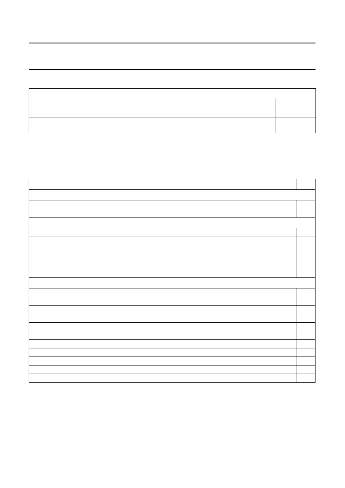
ORDERING INFORMATION
TYPE NUMBER
NAME DESCRIPTION VERSION
TDA8366 SDIP52 plastic shrink dual in-line package; 52 leads (600 mil) SOT247-1
(1)
TDA8366H QFP64
plastic quad flat package; 64 leads (lead length 1.95 mm);
body 14 × 20 × 2.8 mm
Note
1. When using IR reflow soldering it is recommended that the Drypack instructions in the
(order number 9398 510 63011) are followed.
QUICK REFERENCE DATA
SYMBOL PARAMETER MIN. TYP. MAX. UNIT
Supply
V
P
I
P
supply voltage − 8.0 − V
supply current − 100 − mA
Input voltages
V
46,47(rms)
V
15(p-p)
V
9(p-p)
V
8(p-p)
video IF amplifier sensitivity (RMS value) − 70 −µV
external CVBS input (peak-to-peak value) − 1.0 − V
S-VHS luminance input voltage (peak-to-peak value) − 1.0 − V
S-VHS chroma input voltage (burst amplitude)
(peak-to-peak value)
V
21,22,23(p-p)
RGB inputs (peak-to-peak value) − 0.7 − V
Output signals
V
o(p-p)
I
52
V
36(p-p)
V
13(p-p)
V
28(p-p)
V
27(p-p)
V
26
V
19,18,17(p-p)
I
38
I
44,45
I
43
demodulated CVBS output (peak-to-peak value) − 2.5 − V
tuner AGC output current range 0 − 5mA
TXT output voltage (peak-to-peak value) − 1.0 − V
PIP output voltage (peak-to-peak value) − 1.0 − V
−(R−Y) output voltage (peak-to-peak value) − 525 − mV
−(B−Y) output voltage (peak-to-peak value) − 675 − mV
Y output voltage − 450 − mV
RGB output signal amplitudes (peak-to-peak value) − 2.0 − V
horizontal output current 10 −−mA
vertical output current 1 −−mA
EW drive output current 0.5 −−mA
PACKAGE
“Quality Reference Handbook”
− 0.3 − V
SOT319-2
January 1995 3
Page 4
Philips Semiconductors Objective specification
I2C-bus controlled PAL/NTSC TV
processor
BLOCK DIAGRAM
(pos)
(neg)
VDR
VDR
EHTO
EWD
DIG
DEC
FBI
SCO
PH2LF
BG
DEC
HOUT
43
EW GEOMETRY
HORIZONTAL
2nd LOOP AND
ref
7310 35 40 39 37 38
AND
VCO
48
OUTPUT
CONTROL
49
45
44
VERTICAL
GEOMETRY
DIVIDER
VERTICAL
HORIZONTAL/
SYNC
SEPARATOR
AND 1st LOOP
VSC
50
ref
I
BLKIN
16
BLACK
CURRENT
STABILIZER
WHITE
SYNC
VERTICAL
SEPARATOR
BCLIN
20
191817
BRI CONTR
POINT
ref
BO
RO
GO
AND
OUTPUT
RGB MATRIX
AND
DELAY
PEAKING
FILTER
TUNING
AND
SWITCH
RGB INPUT
AND
G-Y MATRIX
SAT CONTROL
28 27 30 29 26 25 21 22 23 24
PAL/NTSC
DECODER
34 33 32
MLA745 - 1
DET
RYO BYO BYIRYI
RI GI BI
RGBIN
LUMIN
3.6
MHz
4.4
MHz
TDA8366
LUMOUT
TDA4661
XTAL2 XTAL1
PH1LF
SCL SDA
P2
V ( 8 V)
P1
V ( 8 V)
2
I C-BUS
56 41
TRANSCEIVER
TOP
AGC FOR IF
AND TUNER
51
52
(TUNER)
AGCOUT
POL
AGC
DEC
2 x 4 bits
17 x 6 bits
CONTROL DACs
POL
IF AMPLIFIER
AND DEMODULATOR
2
46
47
IFDEM2
IFIN1
IFIN2
TDA8366
VIDEO
AMPLIFIER
1
IFDEM1
BANDPASSTRAP
MUTE
VIDEO MUTE
IDENT
AFC AND
SAMPLE AND HOLD
AFC
HUE
SW SAT
S-VHS - SWITCH
SW
CVBS - SWITCH
VIDEO
IDENTIFICATION
8 9 13 36 14 31
411 15
4212
FT
DEC
INT
CVBSIFVO
GND2
GND1
PIPO
EXT
CVBS
CVBS/TXT
CVBS/Y
CHROMA
TRAP
SOUND
ref
SEC
handbook, full pagewidth
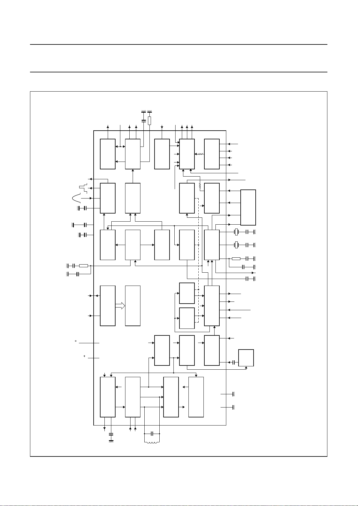
Fig.1 Block diagram (SDIP52; SOT247-1).
January 1995 4
Page 5

Philips Semiconductors Objective specification
I2C-bus controlled PAL/NTSC TV
processor
PINNING
SYMBOL
SDIP52 QFP64
IFDEM1 1 11 IF demodulator tuned circuit 1
IFDEM2 2 12 IF demodulator tuned circuit 2
DEC
DIG
IFVO 4 14 IF video output
SCL 5 16 serial clock input
SDA 6 17 serial data input/output
DEC
BG
CHROMA 8 20 chrominance input (S-VHS)
CVBS/Y 9 21 external CVBS/Y input
V
P1
CVBS
INT
10 22 main supply voltage 1 (+8 V)
11 29 internal CVBS input
GND1 12 25 ground 1
PIPO 13 27 picture-in-picture output
DEC
CVBS
FT
EXT
14 28 decoupling filter tuning
15 24 external CVBS input
BLKIN 16 30 black-current input
BO 17 31 blue output
GO 18 32 green output
RO 19 33 red output
BCLIN 20 35 beam current limiter input
RI 21 37 red input for insertion
GI 22 38 green input for insertion
BI 23 39 blue input for insertion
RGBIN 24 40 RGB insertion input
LUMIN 25 42 luminance input
LUMOUT 26 43 luminance output
BYO 27 44 (B−Y) signal output
RYO 28 45 (R−Y) signal output
BYI 29 46 (B−Y) signal input
RYI 30 47 (R−Y) signal input
SEC
ref
31 48 SECAM reference output
XTAL1 32 49 3.58 MHz crystal connection
XTAL2 33 50 4.43/3.58 MHz crystal connection
DET 34 52 loop filter phase detector
V
P2
35 54 horizontal oscillator supply voltage (+8 V)
CVBS/TXT 36 55 CVBS/TXT output
SCO 37 56 sandcastle output
HOUT 38 57 horizontal output
PIN
DESCRIPTION
3 13 decoupling digital supply
7 18 bandgap decoupling
TDA8366
January 1995 5
Page 6

Philips Semiconductors Objective specification
I2C-bus controlled PAL/NTSC TV
processor
SYMBOL
FBI 39 58 flyback input
PH2LF 40 59 phase-2 filter
PH1LF 41 60 phase-1 filter
GND2 42 26 ground 2
EWD 43 63 east-west drive output
VDR
(pos)
VDR
(neg)
IFIN1 46 2 IF input 1
IFIN2 47 3 IF input 2
EHTO 48 4 EHT/overvoltage protection input
VSC 49 5 vertical sawtooth capacitor
I
ref
DEC
AGC
AGCOUT 52 8 tuner AGC output
n.c. − 9 not connected
n.c. − 10 not connected
n.c. − 15 not connected
n.c. − 19 not connected
n.c. − 34 not connected
n.c. − 36 not connected
n.c. − 41 not connected
n.c. − 51 not connected
n.c. − 53 not connected
V
P3
GND3 − 61 ground 3
GND4 − 62 ground 4
SDIP52 QFP64
44 64 vertical drive 1 positive output
45 1 vertical drive 2 negative output
50 6 reference current input
51 7 AGC decoupling capacitor
PIN
DESCRIPTION
− 23 supply voltage 3 (+8 V)
TDA8366
The pin numbers mentioned in the rest of this document are referenced to the SDIP52 (SOT247-1) package.
January 1995 6
Page 7

Philips Semiconductors Objective specification
I2C-bus controlled PAL/NTSC TV
processor
handbook, halfpage
DEC
CHROMA
CVBS
CVBS
LUMOUT
IFDEM1
IFDEM2
DEC
CVBS/Y
DEC
RGBIN
LUMIN
1
2
3
DIG
4
IFVO
SCL
5
6
SDA
7
BG
8
9
V
10
P1
11
INT
12
GND1
PIPO
13 40
14
FT
15
EXT
16
BLKIN
17
BO
18
GO
19
RO
20
BCLIN
21
RI
22
GI
23
BI
24
25
26
TDA8366
MLA737 - 1
52
51
50
49
48
47
46
45
44
43
42
41
39
38
37
36
35
34
33
32
31
30
29
28
27
AGCOUT
DEC
AGC
I
ref
VSC
EHTO
IFIN2
IFIN1
VDR
(neg)
VDR
(pos)
EWD
GND2
PH1LF
PH2LF
FBI
HOUT
SCO
CVBS/TXT
V
P2
DET
XTAL2
XTAL1
SEC
ref
RYI
BYI
RYO
BYO
TDA8366
Fig.2 Pin configuration (SDIP52).
January 1995 7
Page 8

Philips Semiconductors Objective specification
I2C-bus controlled PAL/NTSC TV
processor
handbook, full pagewidth
VDR
(neg)
IFIN1
IFIN2
EHTO
VSC
I
DEC
AGC
AGCOUT
n.c.
n.c.
IFDEM1
IFDEM2
DEC
DIG
IFVO
ref
(pos)
VDR
EWD
GND4
64
63
62
1
2
3
4
5
6
7
8
9
10
11
12
13
14
GND3
61
PH1LF
60
TDA8366H
PH2LF
59
FBI
58
HOUT
57
SCO
56
P2
V
CVBS/TXT
55
54
n.c.
53
DET
52
51
50
49
48
47
46
45
44
43
42
41
40
39
38
n.c.
XTAL2
XTAL1
SEC
ref
RYI
BYI
RYO
BYO
LUMOUT
LUMIN
n.c.
RGBIN
BI
GI
TDA8366
n.c.
15
SCL
16
SDA
17
DEC
BG
n.c.
18
19
20
21
CVBS/Y
CHROMA
22
P1
V
24
EXT
CVBS
25
GND1
23
P3
V
Fig.3 Pin configuration (QFP64).
January 1995 8
26
GND2
27
PIPO
28
FT
DEC
29
INT
CVBS
30
BLKIN
31
BO
32
GO
37
36
35
34
33
MLC756
RI
n.c.
BCLIN
n.c.
RO
Page 9

Philips Semiconductors Objective specification
I2C-bus controlled PAL/NTSC TV
processor
FUNCTIONAL DESCRIPTION
Vision IF amplifier
The IF-amplifier contains 3 AC-coupled control stages with
a total gain control range which is in excess of 66 dB. The
sensitivity of the circuit is comparable with that of modern
IF-ICs. The reference carrier for the video demodulator is
obtained by means of passive regeneration of the picture
carrier. The external reference tuned circuit is the only
remaining adjustment of the IC.
The polarity of the demodulator can be switched via the
2
I
C-bus in such a way that the circuit is suitable for both
positive and negative modulated signals.
The AFC-circuit is driven with the same reference signal as
the video demodulator. To avoid that the video content
disturbs the AFC operation a sample-and-hold circuit is
applied for signals with negative modulation. The capacitor
for this function is internal. The AFC information is supplied
to the tuning system via the I2C-bus.
The AGC-detector operates on top-sync or top white-level
depending on the polarity of the demodulator. The
demodulation polarity is switched via the I2C-bus. The
AGC detector time-constant capacitor is connected
externally (this mainly because of the flexibility of the
application). The time-constant of the AGC system during
positive modulation is rather long to avoid visible variations
of the signal amplitude. To obtain an acceptable speed of
the AGC system a circuit has been included which detects
whether the AGC detector is activated every frame period.
When during 3 frame periods no action is detected the
speed of the system is increased.
The circuit contains a video identification circuit which is
independent of the synchronization circuit. Therefore
search tuning is possible when the display section of the
receiver is used as a monitor. The identification output is
supplied to the tuning system via the I2C-bus. The
information of this identification circuit can also be used to
switch the phase-1 (ϕ1) loop to a low gain when no signal
is received so that a stable OSD display is obtained. The
coupling of the video identification circuit with the ϕ1loop
can be switched on and off via the I2C-bus.
TDA8366
Synchronization circuit
The sync separator is preceded by a controlled amplifier
which adjusts the sync pulse amplitude to a fixed level.
These pulses are fed to the slicing stage which is operating
at 50% of the amplitude.
The separated sync pulses are fed to the first phase
detector and to the coincidence detector. This coincidence
detector is only used to detect whether the line oscillator is
synchronized and not for transmitter identification. The first
Phase-Locked Loop (PLL) has a very high-statical
steepness so that the phase of the picture is independent
of the line frequency.
The line oscillator is running at twice the line frequency.
The oscillator capacitor is internal. Because of the spreads
of internal components an automatic adjustment circuit
has been added to the IC. It compares the oscillator
frequency with that of the crystal oscillator in the colour
decoder.
To protect the horizontal output transistor the horizontal
drive is switched-off when a power-on-reset is detected.
The frequency of the oscillator is calibrated again when all
subaddress bytes have been sent. When the oscillator has
the right frequency the calibration stops and the horizontal
drive is switched-on again via the soft start procedure
(standby bit in normal mode). When the IC is switched-on
the same procedure is followed.
When the coincidence detector indicates an out-of-lock
situation the calibration procedure is repeated.
The circuit has a second control loop to generate the drive
pulses for the horizontal driver stage. During the start-up
procedure the duty cycle of the horizontal output pulse
increases from 0 to 50% in approximately 100 lines.
The vertical sawtooth generator drives the vertical output
and EW correction drive circuits. The geometry processing
circuits provide control of horizontal shift, EW width, EW
parabola/width ratio, EW corner/parabola ratio, trapezium
correction, vertical shift, vertical slope, vertical amplitude,
and the S-correction. All these controls can be set via the
2
C-bus. The geometry processor has a differential current
I
January 1995 9
Page 10

Philips Semiconductors Objective specification
I2C-bus controlled PAL/NTSC TV
processor
output for the vertical drive signal and a single-ended
output for the EW drive. Both the vertical drive and the EW
drive outputs can be modulated for EHT compensation.
The EHT compensation pin is also used for overvoltage
protection.
The geometry processor also offers the possibilities for
vertical compression (for display of 16 : 9 pictures on a
4 : 3 screen) and vertical expansion (for display of
4 : 3 pictures on a 16 : 9 screen with full picture width, or
for display of ‘letter-box’ transmissions on a 4 : 3 screen
with full picture height). For the expand mode it is possible
to shift the picture vertically (only one fixed position).
Also the de-interlace of the vertical output can be set via
the I2C-bus.
To avoid damage of the picture tube when the vertical
deflection fails the guard output current of the TDA8350
can be supplied to the sandcastle output. When a failure is
detected the RGB-outputs are blanked and a bit is set
(NDF) in the status byte of the I2C-bus. When no vertical
deflection output stage is connected this guard circuit will
also blank the output signals. This can be overruled by
means of the EVG bit of subaddress 0A (see Table 1).
TDA8366
Video switches
The circuit has two CVBS inputs and an Super-Video
Home System (S-VHS) input. The input can be chosen by
2
the I
C-bus. The input selector also has a position in which
CVBS
S-VHS input. When the input selector is in this position it
switches to the S-VHS input if the S-VHS detector detects
sync pulses on the S-VHS luminance input. The S-VHS
detector output can be read by the I2C-bus. When the
S-VHS option is not used the luminance input can be used
as a second input for external CVBS signals. The choice is
made via the CVS-bit (see Table 1).
The video switch circuit has two outputs which can be
programmed in a different way. The input signal for the
decoder is also available on the TXT output. Therefore this
signal can be used to drive the teletext decoder and the
SECAM add-on decoder. The signal on the PIP output can
be chosen independent of the TXT output. If S-VHS is
selected for one of the outputs the luminance and
chrominance signals are added so that a CVBS signal is
obtained again.
Colour decoder
is processed, unless there is a signal on the
EXT
Integrated video filters
The circuit contains a chrominance bandpass and trap
circuit. The chrominance trap filter in the luminance path is
designed for a symmetrical step response behaviour. The
filters are realized by means of gyrator circuits and they
are automatically tuned by comparing the tuning frequency
with the crystal frequency of the decoder. The luminance
delay line and the delay for the peaking circuit are also
realized by means of gyrator circuits.
It is possible to connect a Colour Transient Improvement
(CTI) or Picture Signal Improvement (PSI) IC to the
TDA8366. Therefore the luminance signal which has
passed the filter and delay line circuit is externally
available. The output signal of the transient improvement
circuit must be supplied to the luminance input circuit.
When the CTI function is not required the two pins must be
AC-coupled.
The colour decoder contains an alignment-free crystal
oscillator, a killer circuit and the colour difference
demodulators. The 90° phase shift for the reference signal
is made internally. The demodulation angle and gain ratio
for the colour difference signals for PAL and NTSC are
adapted to the standard.
The colour decoder is very flexible. Together with the
SECAM decoder TDA8395 an automatic multistandard
decoder can be designed.
Which standard the IC can decode depends on the
external crystals. If a 4.4 MHz and a 3.5 MHz crystal are
used PAL 4.4, NTSC 4.4, NTSC 3.5 and PAL 3.5 can be
decoded. If two 3.5 MHz crystals are used PAL N and M
can be decoded. If one crystal is connected only
PAL/NTSC 4.4 or PAL/NTSC 3.5 can be decoded. The
crystal frequency of the decoder is used to tune the line
oscillator. Therefore the value of the crystal frequency
must be given to the IC via the I
2
C-bus.
January 1995 10
Page 11

Philips Semiconductors Objective specification
I2C-bus controlled PAL/NTSC TV
processor
RGB output circuit and black-current stabilization
The colour-difference signals are matrixed with the
luminance signal to obtain the RGB-signals. For the
RGB-inputs linear amplifiers have been chosen so that the
circuit is suited for signals coming from the SCART
connector. The contrast and brightness control operate on
internal and external signals.
The output signal has an amplitude of approximately 2 V
black-to-white at nominal input signals and nominal
settings of the controls.
The black current stabilization is realized by means of a
feedback from the video output amplifiers to the RGB
control circuit. The ‘black current’ of the 3 guns of the
picture tube is internally measured and stabilized. The
black level control is active during 4 lines at the end of the
vertical blanking. During the first line the leakage current is
measured and the following 3 lines the 3 guns are
adjusted to the required level. The maximum acceptable
leakage current is ±100 µA. The nominal value of the
‘black current’ is 10 µA. The ratio of the currents for the
various guns automatically tracks with the white point
adjustment so that the back-ground colour is the same as
the adjusted white point.
TDA8366
visible on the screen. As soon as the current supplied to
the measuring input exceeds a value of 190 µA the
stabilization circuit is activated. After a waiting time of
approximately 0.8 s the blanking and the beam current
limiting input pin are released. The remaining switch-on
behaviour of the picture is determined by the external time
constant of the beam current limiting network.
2
C-BUS SPECIFICATION
I
handbook, halfpage
X =don’t care.
Valid subaddresses: 00 to 13; subaddress FE is reserved
for test purposes. Auto-increment mode is available for
subaddresses.
A6 A5 A4 A3 A2 A1 A0
1000101X
R/W
MLA743
Fig.4 Slave address (8A).
The input impedance of the ‘black-current’ measuring pin
is 15 kΩ. Therefore the beam current during scan will
cause the input voltage to exceed the supply voltage. The
internal protection will start conducting so that the
excessive current is bypassed.
When the TV receiver is switched-on the black current
stabilization circuit is not active, the RGB outputs are
blanked and beam current limiting input pin is
short-circuited. Only during the measuring lines will the
outputs supply a voltage of 5 V to the video output stage
so that it can be detected if the picture tube is warming up.
These pulses are switched-on after a waiting time of
approximately 0.5 s. This ensures that the vertical
deflection is activated so that the measuring pulses are not
Start-up procedure
Read the status bytes until POR = 0 and send all
subaddress bytes. The horizontal output signal is
switched-on when the oscillator is calibrated. It is possible
to have the horizontal output signal available before
calibration. Then the SFM bit must be set to logic 0.
Each time before the data in the IC is refreshed, the status
bytes must be read. If POR = 1, the procedure mentioned
above must be carried out to restart the IC.
When this procedure is not followed the horizontal
frequency may be incorrect after power-up or after a
power dip.
January 1995 11
Page 12

Philips Semiconductors Objective specification
I2C-bus controlled PAL/NTSC TV
TDA8366
processor
Inputs
Table 1 Input status bits; note 1
FUNCTION
Source select 00 INA INB INC IND FOA FOB XA XB
Decoder mode 01 FORF FORS DL STB POC CM2 CM1 CM0
Hue 02 X X A5 A4 A3 A2 A1 A0
Horizontal shift (HS) 03 X X A5 A4 A3 A2 A1 A0
EW width (EW) 04 X X A5 A4 A3 A2 A1 A0
EW parabola/width (PW) 05 X X A5 A4 A3 A2 A1 A0
EW corner parabola (CP) 06 X X A5 A4 A3 A2 A1 A0
EW trapezium (TC) 07 X X A5 A4 A3 A2 A1 A0
Vertical slope (VS) 08 NCIN X A5 A4 A3 A2 A1 A0
Vertical amplitude (VA) 09 VID LBM A5 A4 A3 A2 A1 A0
S-correction (SC) 0A HCO EVG A5 A4 A3 A2 A1 A0
Vertical shift (VSH) 0B SBL PRD A5 A4 A3 A2 A1 A0
White point R 0C EXP CL A5 A4 A3 A2 A1 A0
White point G 0D SFM CVS A5 A4 A3 A2 A1 A0
White point B 0E MAT PHL A5 A4 A3 A2 A1 A0
Peaking 0F YD3 YD2 YD1 YD0 A3 A2 A1 A0
Brightness 10 RBL COR A5 A4 A3 A2 A1 A0
Saturation 11 IE1 X A5 A4 A3 A2 A1 A0
Contrast 12 AFW IFS A5 A4 A3 A2 A1 A0
AGC take-over 13 MOD VSW A5 A4 A3 A2 A1 A0
SUBADDRESS
(HEX)
D7 D6 D5 D4 D3 D2 D1 D0
DATA BYTE
Note
1. X = don’t care.
Table 2 Output status bits; note 1
FUNCTION
Output status bytes 00 POR FSI STS SL XPR CD2 CD1 CD0
Note
1. X = don’t care.
January 1995 12
SUBADDRESS
(HEX)
01 NDF IN1 X IFI AFA AFB X X
D7 D6 D5 D4 D3 D2 D1 D0
DATA BYTE
Page 13
Philips Semiconductors Objective specification
I2C-bus controlled PAL/NTSC TV
processor
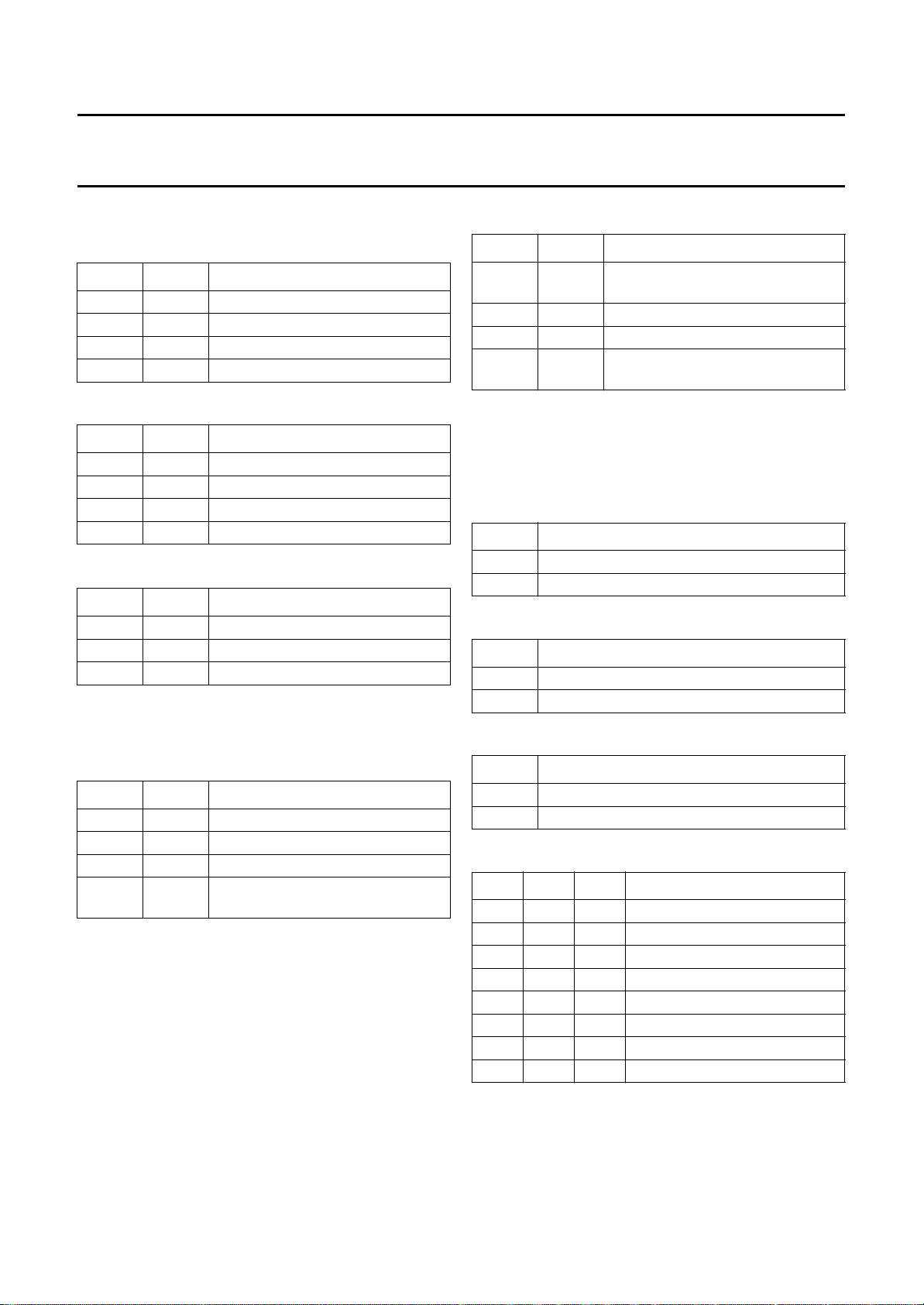
INPUT CONTROL BITS
Table 3 Source select 1
INA INB DECODER AND TXT
0 0 CVBS
0 1 CVBS
1 0 S-VHS
1 1 S-VHS (CVBS
Table 4 Source select 2
INC IND PIP
0 0 CVBS
0 1 CVBS
1 0 S-VHS
1 1 S-VHS (CVBS
Table 5 Phase 1 (ϕ1) time constant
FOA FOB
(1)
0 0 normal
0 1 slow
1 X fast
Note
1. X = don’t care.
Table 6 Crystal indication
XA XB CRYSTAL
0 0 two 3.6 MHz
0 1 one 3.6 MHz (pin 32)
1 0 one 4.4 MHz (pin 33)
1 1 3.6 MHz (pin 32) and 4.4 MHz
(pin 33)
INT
EXT
INT
EXT
)
EXT
)
EXT
MODE
TDA8366
Table 7 Forced field frequency
FORF FORS FIELD FREQUENCY
0 0 auto (60 Hz when line not
synchronized)
0 1 60 Hz; note 1
1 0 50 Hz; note 1
1 1 auto (50 Hz when line not
synchronized)
Note
1. When the forced mode is selected the divider will only
switch to that position when the horizontal oscillator is
not synchronized.
Table 8 Interlace
DL STATUS
0 interlace
1 de-interlace
Table 9 Standby
STB MODE
0 standby
1 normal
Table 10 Synchronization mode
POC MODE
0 active
1 not active
Table 11 Colour decoder mode
CM2 CM1 CM0 DECODER MODE
0 0 0 not forced, own intelligence
0 0 1 forced NTSC 3.6 MHz
0 1 0 forced PAL 4.4 MHz
0 1 1 forced SECAM
1 0 0 forced NTSC 4.4 MHz
1 0 1 forced PAL 3.6 MHz (pin 32)
1 1 0 forced PAL 3.6 MHz (pin 33)
1 1 1 no function
January 1995 13
Page 14

Philips Semiconductors Objective specification
I2C-bus controlled PAL/NTSC TV
processor
Table 12 Vertical divider mode
NCIN VERTICAL DIVIDER MODE
0 normal operation
1 switched to search window
Table 13 Video ident mode
VID VIDEO IDENT MODE
0 ϕ
1 not active
Table 14 Long blanking mode
LBM BLANKING MODE
0 adapted to standard (50 or 60 Hz)
1 fixed in accordance with 50 Hz standard
Table 15 EHT tracking mode
loop switched on and off
1
TDA8366
Table 20 Horizontal frequency during switch-on
SFM START-UP FREQUENCY
0 maximum
1 nominal
Table 21 Condition Y/C input
CVS Y-INPUT MODE
0 switched to Y/C mode
1 switched to CVBS mode
Table 22 PAL/NTSC matrix
MAT MATRIX
0 adapted to standard
1PAL
Table 23 Colour crystal PLL
HCO TRACKING MODE
0 EHT tracking only on vertical
1 EHT tracking on vertical and EW
Table 16 Enable vertical guard (RGB blanking)
EVG VERTICAL GUARD MODE
0 not active
1 active
Table 17 Service blanking
SBL SERVICE BLANKING MODE
0off
1on
Table 18 Overvoltage input mode
PRD OVERVOLTAGE MODE
0 detection mode
1 protection mode
Table 19 Vertical deflection mode
PHL STATE
0 PLL closed
1 oscillator free-running
Table 24 Y-delay adjustment; note 1
YD0 to YD3 Y-DELAY
YD3 YD3 ∗ 160 ns +
YD2 YD2 ∗ 80 ns +
YD1 YD1 ∗ 40 ns +
YD0 YD0 ∗ 40 ns
Note
1. For an equal delay of the luminance and chrominance
signal the delay must be set at a value of 160 ns. This
is only valid for a CVBS signal without group
delay distortions.
Table 25 RGB blanking
RBL RGB BLANKING
0 not active
1 active
EXP CL VERTICAL DEFLECTION MODE
0 0 normal
0 1 compress
1 0 expand
1 1 expand and lift
January 1995 14
Table 26 Noise coring (peaking)
COR NOISE CORING
0off
1on
Page 15
Philips Semiconductors Objective specification
I2C-bus controlled PAL/NTSC TV
processor
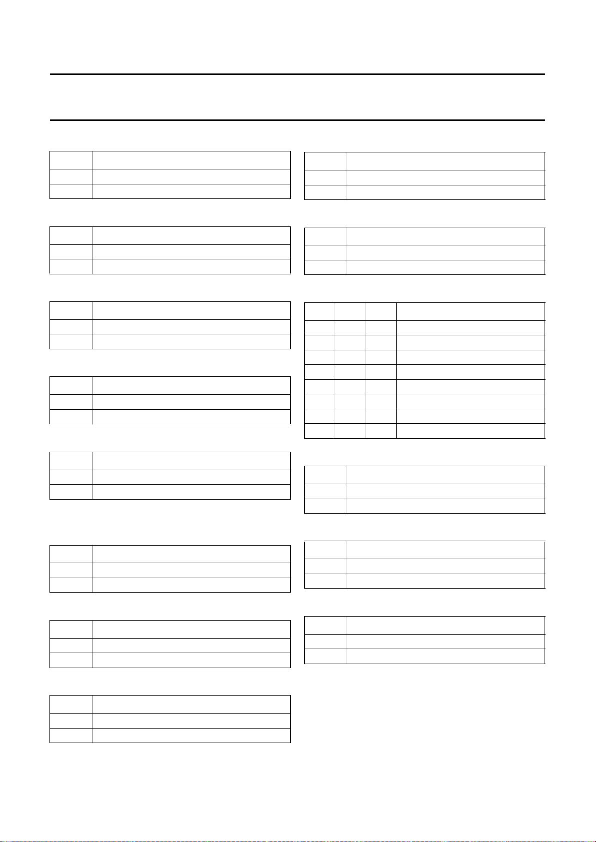
Table 27 Enable fast blanking
IE1 FAST BLANKING
0 not active
1 active
Table 28 AFC window
AFW AFC WINDOW
0 normal
1 enlarged
Table 29 IF sensitivity
IFS IF SENSITIVITY
0 normal
1 reduced
Table 30 Modulation standard
MOD MODULATION
0 negative
1 positive
Table 31 Video mute
VSW STATE
0 normal operation
1 IF-video signal switched off
O
UTPUT CONTROL BITS
Table 32 Power-on-reset
POR MODE
0 normal
1 power-down
TDA8366
Table 35 Phase 1 (ϕ1) lock indication
SL INDICATION
0 not locked
1 locked
Table 36 X-ray protection
XPR OVERVOLTAGE
0 no overvoltage detected
1 overvoltage detected
Table 37 Colour decoder mode
CD2 CD1 CD0 STANDARD
0 0 0 no colour standard identified
0 0 1 NTSC 3.6 MHz
0 1 0 PAL 4.4 MHz
0 1 1 SECAM
1 0 0 NTSC 4.4 MHz
1 0 1 PAL 3.6 MHz (pin 32)
1 1 0 PAL 3.6 MHz (pin 33)
1 1 1 spare
Table 38 Output vertical guard
NDF VERTICAL OUTPUT STAGE
0OK
1 failure
Table 39 Indication RGB insertion
IN1 RGB INSERTION
0 no (pin 24 LOW)
1 yes (pin 24 HIGH)
Table 33 Field frequency indication
FSI FREQUENCY
050Hz
160Hz
Table 34 S-VHS status
STS S-VHS INPUT
0 no signal
1 signal
January 1995 15
Table 40 Output video identification
IFI VIDEO SIGNAL
0 no video signal identified
1 video signal identified
Page 16

Philips Semiconductors Objective specification
I2C-bus controlled PAL/NTSC TV
TDA8366
processor
Table 41 AFC output
AFA AFB CONDITION
0 0 outside window; too low
0 1 outside window; too high
1 0 in window; below reference
1 1 in window; above reference
LIMITING VALUES
In accordance with the Absolute Maximum Rating System (IEC 134).
SYMBOL PARAMETER CONDITIONS MIN. MAX. UNIT
V
P
T
stg
T
amb
T
sol
T
j
V
es
supply voltage − 9.0 V
storage temperature −25 +150 °C
operating ambient temperature 0 70 °C
soldering temperature for 5 s − 260 °C
operating junction temperature − 150 °C
electrostatic handling HBM; all pins; notes 1 and 2 −2000 +2000 V
MM; all pins; notes 1 and 3 −200 +200 V
Notes
1. All pins are protected against ESD by means of internal clamping diodes.
2. Human Body Model (HBM): R = 1.5 kΩ; C = 100 pF.
3. Machine Model (MM): R = 0 Ω; C = 200 pF.
THERMAL CHARACTERISTICS
SYMBOL PARAMETER VALUE UNIT
R
th j-a
thermal resistance from junction to ambient in free air
SDIP52 40 K/W
QFP64 50 K/W
QUALITY SPECIFICATION
In accordance with
“SNW-FQ-611E”
. The number of the
quality specification can be found in the
Reference Handbook”
. The handbook can be ordered
using the code 9398 510 63011.
Latch-up
• I
• I
≥ 100 mA or ≥1.5V
trigger
≤−100 mA or ≤−0.5V
trigger
DD(max)
DD(max)
.
“Quality
Following pins do not meet the above specification:
Pin 7: −90 mA
Pin 17: 90 mA
Pin 18: 90 mA
Pin 19: 90 mA
Pin 24: −90 mA
Pin 34: 60 mA
Pin 49: −90 mA
Pin 50: ±90 mA.
January 1995 16
Page 17
Philips Semiconductors Objective specification
I2C-bus controlled PAL/NTSC TV
TDA8366
processor
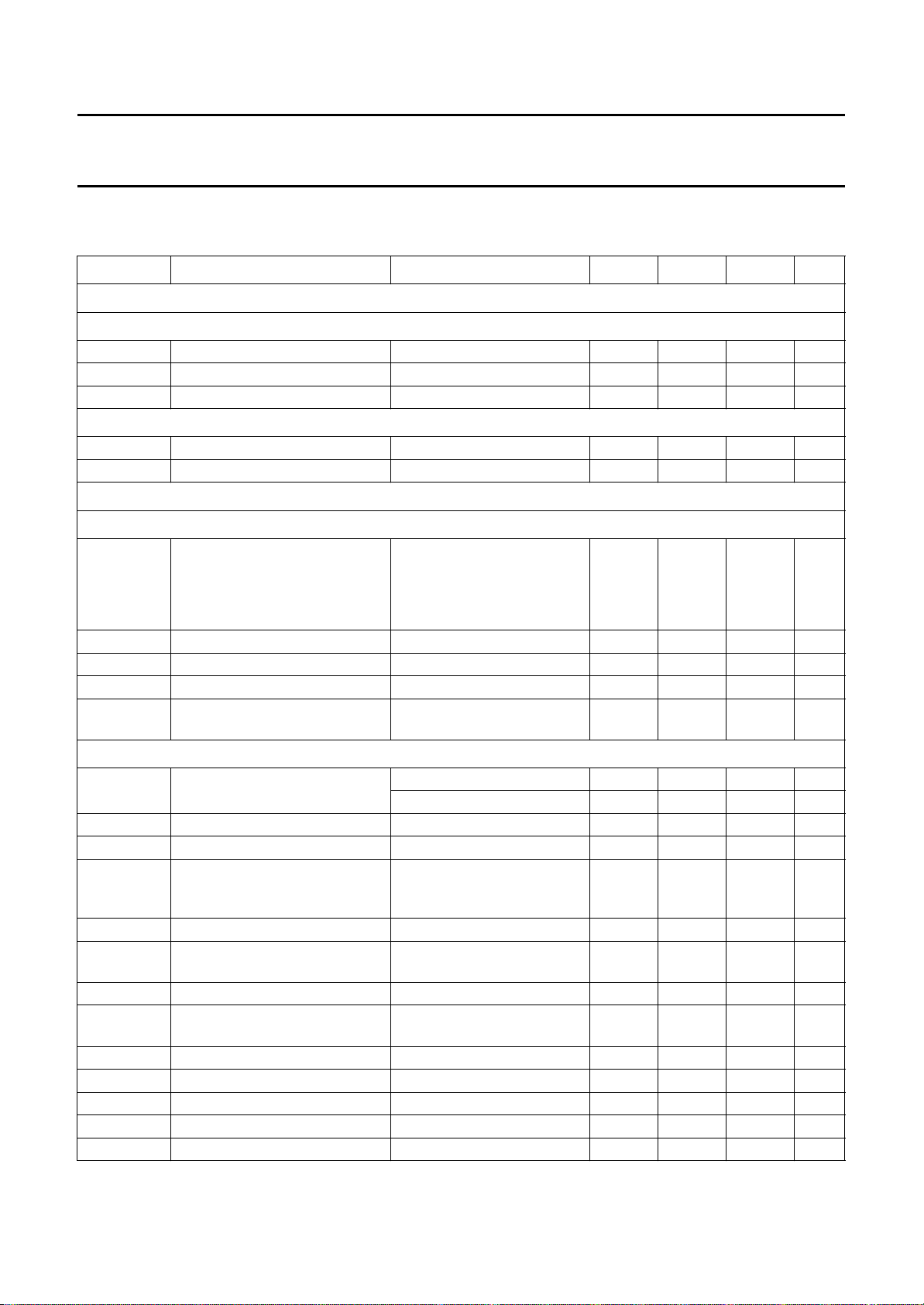
CHARACTERISTICS
V
=8V; T
P
SYMBOL PARAMETER CONDITIONS MIN. TYP. MAX. UNIT
Supplies
M
AIN SUPPLY (PIN 10)
V
P1
I
P1
P
tot
HORIZONTAL OSCILLATOR SUPPLY (PIN 35)
V
P2
I
P2
IF circuit
V
ISION IF AMPLIFIER INPUTS (PINS 46 AND 47)
V
i(rms)
R
I
C
I
G
cr
V
i max(rms)
VIDEO AMPLIFIER OUTPUT (PIN 4); note 3
V
o
V
4
V
4
∆V
4
Z
o
I
bias
I
source(max)
B bandwidth of demodulated
G
diff
ϕ
diff
NL
vid
V
th
V
ins
=25°C; unless otherwise specified.
amb
supply voltage 7.2 8.0 8.8 V
supply current − 100 − mA
total power dissipation − 850 − W
supply voltage 7.2 8.0 8.8 V
supply current − 6 − mA
input sensitivity (RMS value) note 1
= 38.90 MHz − 70 100 µV
f
i
= 45.75 MHz − 70 100 µV
f
i
= 58.75 MHz − 70 100 µV
f
i
input resistance (differential) note 2 − 2 − kΩ
input capacitance (differential) note 2 − 3 − pF
gain control range 64 −−dB
maximum input signal
100 150 − mV
(RMS value)
zero signal output level negative modulation; note 4 − 4.7 − V
positive modulation; note 4 − 2.0 − V
top sync level negative modulation 1.9 2.0 2.1 V
white level positive modulation − 4.5 − V
difference in amplitude between
− 015%
negative and positive
modulation
video output impedance − 50 −Ω
internal bias current of NPN
1.0 −−mA
emitter follower output transistor
maximum source current −−5mA
at −3dB 6 9 − MHz
output signal
differential gain note 5 − 25%
differential phase notes 5 and 6 −−5 deg
video non-linearity note 7 −−5%
white spot threshold level − 5.0 − V
white spot insertion level − 3.3 − V
January 1995 17
Page 18
Philips Semiconductors Objective specification
I2C-bus controlled PAL/NTSC TV
TDA8366
processor
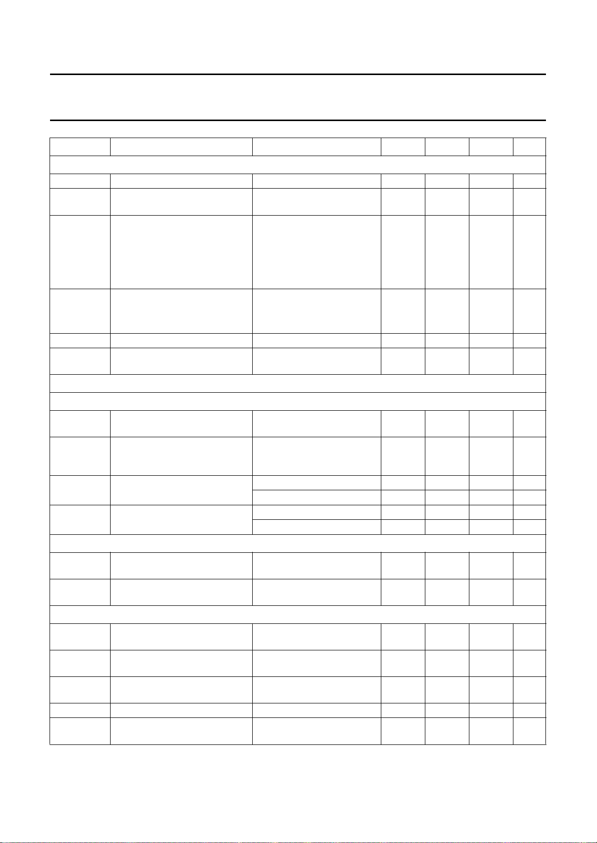
SYMBOL PARAMETER CONDITIONS MIN. TYP. MAX. UNIT
VIDEO AMPLIFIER OUTPUT (CONTINUED)
N
clamp
N
ins
δ
mod
S/N signal-to-noise ratio notes 6 and 9
V
4
V
4
IF AND TUNER AGC; note 10
noise inverter clamping level − 1.4 − V
noise inverter insertion level
− 2.6 − V
(identical to black level)
intermodulation notes 6 and 8
blue V
yellow V
= 0.92 or 1.1 MHz 60 66 − dB
o
= 2.66 or 3.3 MHz 60 66 − dB
V
o
= 0.92 or 1.1 MHz 56 62 − dB
o
= 2.66 or 3.3 MHz 60 66 − dB
V
o
=10mV 52 60 − dB
V
i
end of control range 52 61 − dB
residual carrier signal note6 − 5.5 − mV
residual 2nd harmonic of carrier
note 6 − 2.5 − mV
signal
timing of IF-AGC with a 2.2µF capacitor (pin 51)
modulated video interference 30% AM for 1 mV to 100 mV;
t
inc
response time to an IF input
signal amplitude increase of
52 dB
t
dec
response to an IF input signal
amplitude decrease of 52 dB
I
L
allowed leakage current of the
AGC capacitor
Tuner take-over adjustment (via I2C-bus)
V
51min(rms)
minimum starting level for tuner
take-over (RMS value)
V
51max(rms)
maximum starting level for tuner
take-over (RMS value)
Tuner control output (pin 52)
V
52max
maximum tuner AGC output
voltage
V
52(sat)
I
52max
output saturation voltage minimum tuner gain;
maximum tuner AGC output
swing
I
L
∆V
i
leakage current RF AGC −−1µA
input signal variation for
complete tuner control
−−10 %
0 to 200 Hz (system B/G)
positive and negative
− 2 − ms
modulation
negative modulation − 50 − ms
positive modulation − 100 − ms
negative modulation −−10 µA
positive modulation −−200 nA
− 0.4 0.8 mV
40 80 − mV
maximum tuner gain; note 2 −−V
+1 V
P
−−300 mV
I47=2mA
5 −−mA
0.5 2 4 dB
January 1995 18
Page 19
Philips Semiconductors Objective specification
I2C-bus controlled PAL/NTSC TV
TDA8366
processor
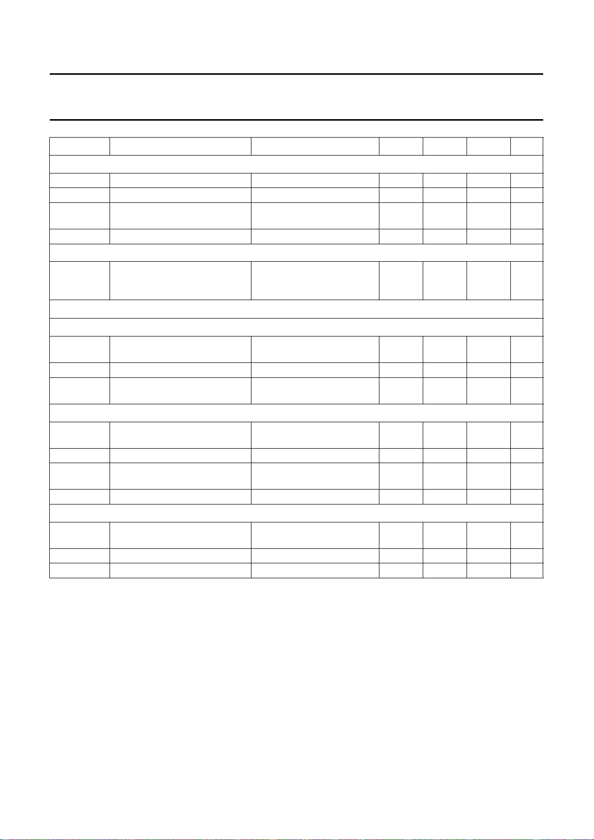
SYMBOL PARAMETER CONDITIONS MIN. TYP. MAX. UNIT
AFC OUTPUT (VIA I2C-BUS); note 11
RES AFC resolution − 2 − bits
W
sen
W
senL
f
os
VIDEO IDENTIFICATION OUTPUT (VIA I2C-BUS)
t
d
CVBS and S-VHS input switch
I
NTERNAL AND EXTERNAL CVBS INPUTS (PINS 11 AND 15)
V
11(p-p)
I
11
SS
CVBS
S-VHS INPUT (PINS 8 AND 9)
V
9(p-p)
I
9(p-p)
V
8
I
8
TXT AND PIP OUTPUT SIGNALS (PINS 36 AND 13)
V
o(p-p)
Z
o
V
TS
window sensitivity 65 80 100 kHz
window sensitivity in large
195 240 300 kHz
window mode
AFC offset note 6 −−50 kHz
delay time of identification after
−−10 ms
the AGC has stabilized on a
new transmitter
CVBS input voltage
note 12 − 1.0 1.4 V
(peak-to-peak value)
CVBS input current − 4 −µA
suppression of non-selected
notes 6 and 13 50 −−dB
CVBS input signal
luminance input voltage
− 1.0 1.4 V
(peak-to-peak value)
luminance input current − 4 −µA
chrominance input voltage
note 14 − 0.3 0.45 V
(burst amplitude)
chrominance input current − 4 −µA
output signal amplitude
− 1.0 − V
(peak-to-peak value)
output impedance −−250 Ω
top sync level − 2.5 − V
January 1995 19
Page 20
Philips Semiconductors Objective specification
I2C-bus controlled PAL/NTSC TV
TDA8366
processor
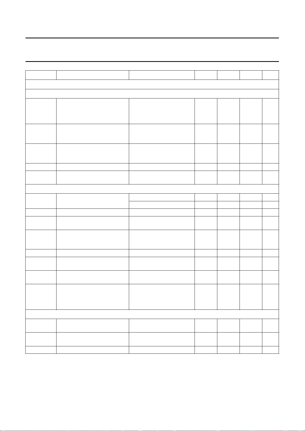
SYMBOL PARAMETER CONDITIONS MIN. TYP. MAX. UNIT
RGB inputs, colour difference inputs, luminance inputs and outputs
RGB INPUTS (PINS 21, 22 AND 23)
V
21,22,23(p-p)
input signal amplitude for an
output signal of 2 V
(black-to-white) (peak-to-peak
value)
V
21,22,23(p-p)
input signal amplitude before
clipping occurs (peak-to-peak
value)
∆V
o
difference between black level
of internal and external signals
at the outputs
I
21,22,23
∆t
d
input currents no clamping; note 2 −−0.5 µA
delay difference for the three
channels
FAST BLANKING (PIN 24)
V
i
V
24(max)
t
d
input voltage no data insertion −−0.4 V
maximum input pulse insertion −−3.0 V
delay time from RGB in to
RGB out
∆t
d
delay difference between
insertion to RGB out and
RGB in to RGB out
I
24
SS
int
input current −−0.2 mA
suppression of internal RGB
signals
SS
ext
suppression of external RGB
signals
V
I
input voltage to blank the RGB
outputs to facilitate ‘On Screen
Display’ signals being applied to
the outputs
COLOUR DIFFERENCE INPUT SIGNALS (PINS 29 AND 30)
V
30(p-p)
input signal amplitude (R−Y)
(peak-to-peak value)
V
29(p-p)
input signal amplitude (B−Y)
(peak-to-peak value)
I
29,30
input current for both inputs note 2 − 0.1 1.0 µA
note 15 − 0.7 0.8 V
note 6 1.0 −−V
−−20 mV
note 6 − 020ns
data insertion 0.9 −−V
data insertion; note 6 − 100 − ns
data insertion; note 6 − 50 − ns
notes 6 and 12; insertion;
55 −−dB
fi= 0 to 5 MHz
notes 6 and 12; no insertion;
55 −−dB
fi= 0 to 5 MHz
4 −−V
note 2 − 1.05 − V
note 2 − 1.35 − V
January 1995 20
Page 21
Philips Semiconductors Objective specification
I2C-bus controlled PAL/NTSC TV
TDA8366
processor
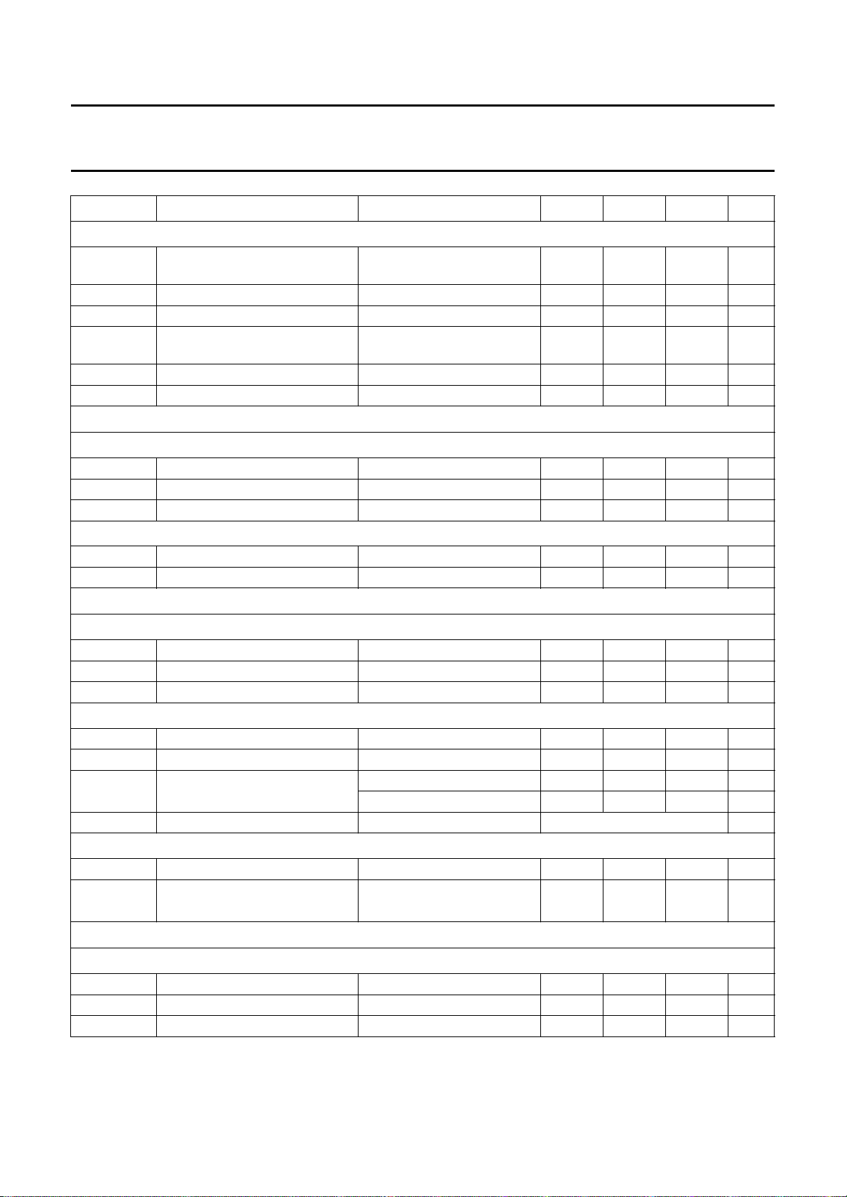
SYMBOL PARAMETER CONDITIONS MIN. TYP. MAX. UNIT
LUMINANCE INPUTS AND OUTPUTS (PINS 25 AND 26)
V
26(p-p)
output signal amplitude
(peak-to-peak value)
V
TS
Z
o
V
25(p-p)
top sync level − 2.5 − V
output impedance − 250 −Ω
input signal amplitude
(peak-to-peak value)
I
clamp
I
i
clamp current during burst key pulse − 200 −µA
input current no clamp −−0.5 µA
Chrominance filters
C
HROMINANCE TRAP CIRCUIT
f
trap
trap frequency − f
QF trap quality factor note 16 − 2 −
SR colour subcarrier rejection 20 −−dB
HROMINANCE BANDPASS CIRCUIT
C
f
c
centre frequency − f
QBP bandpass quality factor − 3 −
top sync-white − 0.45 0.63 V
− 0.45 − V
osc
osc
− MHz
− MHz
Delay line and peaking circuit
Y DELAY LINE
t
d
t
d1
delay time note 6 − 480 − ns
tuning range delay time 8 steps −160 − +160 ns
B bandwidth of internal delay line note 6 5 −−MHz
EAKING CONTROL; note 17
P
f
t
c(p)
W
peaking centre frequency − 3 − MHz
width of preshoot or overshoot note 2 − 160 − ns
OS overshoot positive − 20 − %
negative − 36 − %
peaking control curve 16 steps see Fig.5
ORING STAGE
C
S coring range − 15 − IRE
G
W
wave gain − 1.8 −
negative half wave gain
-------------------------------------------------------------positive half wave gain
Horizontal synchronization circuits
S
YNC VIDEO INPUT (PINS 9, 11 AND 15)
V
9,11,15
SL
SL
HS
VS
sync pulse amplitude note 2 50 300 − mV
slicing level for horizontal sync note 18 − 50 − %
slicing level for vertical sync − 30 − %
January 1995 21
Page 22
Philips Semiconductors Objective specification
I2C-bus controlled PAL/NTSC TV
TDA8366
processor
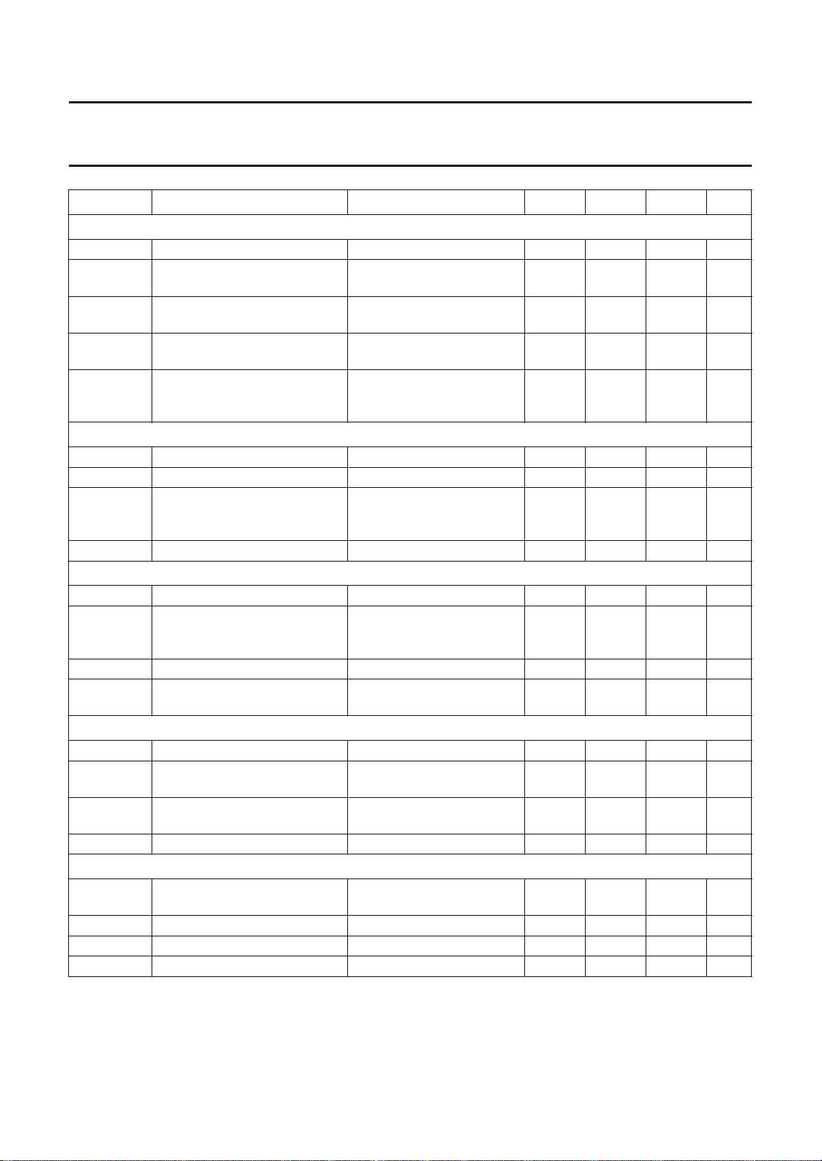
SYMBOL PARAMETER CONDITIONS MIN. TYP. MAX. UNIT
HORIZONTAL OSCILLATOR
f
fr
∆f
fr
∆f/∆V
P
∆f
(max)
∆f
osc(max)
FIRST CONTROL LOOP (FILTER CONNECTED TO PIN 41); note 19
f
HR
f
CR
S/N signal-to-noise ratio of the video
HYS hysteresis at the switching point − 1 − dB
ECOND CONTROL LOOP (CAPACITOR CONNECTED TO PIN 40)
S
∆ϕ
/∆ϕ
i
o
t
cr
t
shift
ORIZONTAL OUTPUT (PIN 38); note 20
H
V
OL
I
O(max)
V
O(max)
δ duty factor note 6 − 50 − %
LYBACK PULSE INPUT (PIN 39)
F
V
HSW
V
ϕ2(SW)
V
39(max)
Z
i
free running frequency − 15625 − Hz
spread on free running
−−±2%
frequency
frequency variation with respect
VP= 8.0 V ±10%; note 6 − 0.2 0.5 %
to the supply voltage
frequency variation with
T
= 0 to 70 °C; note 6 −−80 Hz
amb
temperature
maximum frequency deviation
−−75 %
at the start of the horizontal
output
holding range PLL −±0.9 ±1.2 kHz
catching range PLL note 6 ±0.6 ±0.9 − kHz
− 20 − dB
input signal at which the time
constant is switched
control sensitivity − 150 −µs/µs
control range from start of
11 12 −µs
horizontal output to flyback at
nominal shift position
horizontal shift range 63 steps ±2 −−µs
control sensitivity for dynamic
− 5.3 −µs/V
compensation
LOW level output voltage IO=10mA −−0.3 V
maximum allowed output
10 −−mA
current
maximum allowed output
−−V
P
V
voltage
switching level for horizontal
− 0.4 − V
blanking
switching level for phase-2 loop − 4.0 − V
maximum input voltage note 2 − 8.0 − V
input impedance note 2 − 10 − MΩ
January 1995 22
Page 23
Philips Semiconductors Objective specification
I2C-bus controlled PAL/NTSC TV
TDA8366
processor
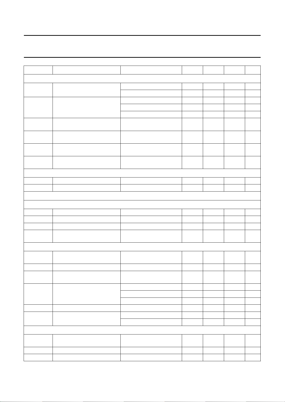
SYMBOL PARAMETER CONDITIONS MIN. TYP. MAX. UNIT
SANDCASTLE PULSE OUTPUT (PIN 37)
V
37
t
W
V
clamp
I
37(min)
I
37(max)
t
d
SOFT START; note 21
δ
df
t
ss
Vertical synchronization and geometry correction
output voltage during burst key 4.8 5.3 5.8 V
during blanking 1.8 2.0 2.2 V
pulse width burst key pulse 3.3 3.5 3.7 µs
vertical blanking (50 Hz) − 25 − lines
vertical blanking (60 Hz) − 21 − lines
clamp level for vertical guard
− 2.7 − V
detection
minimum input current to
−−0.5 mA
activate guard detection
maximum allowable input
2.5 −−mA
current
delay of start of burst key to
− 5.4 −µs
start of sync
duty factor control range 0 − 50 %
soft start time − 100 − lines
V
ERTICAL OSCILLATOR; note 22
f
f
fr
lock
free running frequency − 50/60 − Hz
locking range 45 − 64.5 Hz
divider value not locked − 625/525 − lines
locking range 488 − 722 lines/
frame
ERTICAL RAMP GENERATOR (PIN 49)
V
V
49(p-p)
I
dis
I
charge
sawtooth amplitude
(peak-to-peak value)
discharge current − 1 − mA
charge current set by external
VS = 1FH;
− 3.5 − V
C=100nF;R=39kΩ
note 23 − 19 −µA
resistor
VS vertical slope control range (63 steps) −14 − +14 %
compress mode − 75 − %
expand mode − 133 − %
∆I
V
49
49L
charge current increase f = 60 Hz − 20 − %
LOW level of ramp normal or expand mode − 2.07 − V
compress mode − 2.55 − V
ERTICAL DRIVE OUTPUTS (PINS 44 AND 45)
V
I
diff(p-p)
differential output current
VA = 1FH − 1 − mA
(peak-to-peak value)
I
CM
V
o
common mode current − 400 −µA
output voltage range 0 − 4.0 V
January 1995 23
Page 24
Philips Semiconductors Objective specification
I2C-bus controlled PAL/NTSC TV
TDA8366
processor
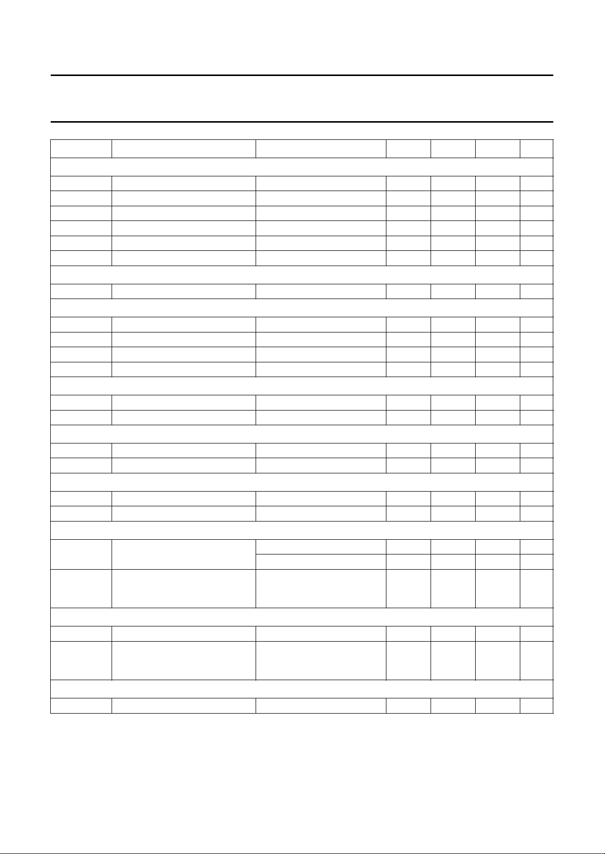
SYMBOL PARAMETER CONDITIONS MIN. TYP. MAX. UNIT
EHT TRACKING/OVERVOLTAGE PROTECTION (PIN 48)
∆V
48
SMR scan modulation range −6 − +6 %
ϕ
vert
ϕ
EW
I
eq
V
48
DE-INTERLACE
EW WIDTH
CR control range 63 steps 100 − 80 %
I
eq
V
o
I
o
EW PARABOLA/WIDTH
CR control range 63 steps 0 − 24 %
I
eq
EW CORNER/PARABOLA
CR control range 63 steps −44 − 0%
I
eq
EW TRAPEZIUM
CR control range 63 steps −4 − +4 %
I
eq
VERTICAL AMPLITUDE
CR control range 63 steps; SC = 00H 80 − 120 %
I
eqdiff(p-p)
VERTICAL SHIFT
CR control range 63 steps −4 − +4 %
I
eqdiff(p-p)
S-CORRECTION
CR control range 63 steps 0 − 25 %
input voltage 1.2 − 2.8 V
vertical sensitivity − 7.5 − %/V
EW sensitivity when switched-on −−7.5 − %/V
EW equivalent output current +120 −−120 µA
overvoltage detection level − 3.9 − V
first field delay − 0.5H −
equivalent output current 0 − 400 µA
EW output voltage range 1.0 − 8.0 V
EW output current range 0 − 900 µA
equivalent output current EW = 3FH 0 − 480 µA
equivalent output current PW = 3FH; EW = 3FH −210 − 0 µA
equivalent output current −80 − +80 µA
63 steps; SC = 3FH 86 − 112 %
equivalent differential vertical
SC = 00H 800 − 1200 µA
drive output current
(peak-to-peak value)
equivalent differential vertical
−40 − +40 µA
drive output current
(peak-to-peak value)
January 1995 24
Page 25
Philips Semiconductors Objective specification
I2C-bus controlled PAL/NTSC TV
TDA8366
processor
SYMBOL PARAMETER CONDITIONS MIN. TYP. MAX. UNIT
Colour demodulation part
CHROMINANCE AMPLIFIER
ACC
cr
∆V change in amplitude of the
THR
on
HYS
off
ACL
CIRCUIT
REFERENCE PART
Phase-locked loop;
f
CR
∆ϕ phase shift for a ±400 Hz
Oscillator
TC
osc
∆f
osc
R
i
C
i
HUE CONTROL
HUE
cr
∆HUE hue variation for ±10% V
∆HUE/∆T hue variation with temperature T
ACC control range note 24 26 −−dB
−−2dB
output signals over the ACC
range
threshold colour killer ON −23 −26 −29 dB
hysteresis colour killer OFF strong signal conditions;
− +3 − dB
S/N ≥ 40 dB; note 6
noisy input signals; note 6 − +1 − dB
chrominance burst ratio at
2.3 − 2.7
which the ACL starts to operate
note 25
catching range 300 500 − Hz
note 6 −−2 deg
deviation of the oscillator
frequency
temperature coefficient of the
note 6 − 2.0 2.5 Hz/K
oscillator frequency
oscillator frequency deviation
note 6; VP=8V±10% −−250 Hz
with respect to the supply
input resistance pin 32; f = 3.58 MHz; note 2 − 1.5 − kΩ
pin 33; f = 4.43 MHz; note 2 − 1.0 − kΩ
input capacitance pins 32 and 33; note 2 −−10 pF
hue control range 63 steps; see Fig.6 ±35 ±40 − deg
P
note 6 − 0 − deg
= 0 to 70 °C; note 6 − 0 − deg
amb
January 1995 25
Page 26
Philips Semiconductors Objective specification
I2C-bus controlled PAL/NTSC TV
TDA8366
processor
SYMBOL PARAMETER CONDITIONS MIN. TYP. MAX. UNIT
DEMODULATORS (PINS 27 AND 28)
V
28(p-p)
(R−Y) output signal amplitude
(peak-to-peak value)
V
27(p-p)
(B−Y) output signal amplitude
(peak-to-peak value)
G gain between both
demodulators G(B−Y) and
G(R−Y)
∆V spread of signal amplitude ratio
PAL/NTSC
Z
o
output impedance (R−Y)/(B−Y)
output
B bandwidth of demodulators −3 dB; note 27 − 650 − kHz
V
27,28(p-p)
residual carrier output
(peak-to-peak value)
V
28(p-p)
H/2 ripple at (R−Y) output
(peak-to-peak value)
/∆T change of output signal
∆V
o
amplitude with temperature
∆V
o
/∆V
change of output signal
P
amplitude with supply voltage
ϕ
e
phase error in the demodulated
signals
COLOUR DIFFERENCE MATRICES IN CONTROL CIRCUIT
note 26 − 0.525 − V
note 26 − 0.675 − V
1.60 1.78 1.96
note 6 −1 − +1 dB
note 6 − 500 −Ω
f=f
; (R−Y) output 5 mV
osc
; (B−Y) output −−5mV
f=f
osc
f=2f
f=2f
; (R−Y) output 5 mV
osc
; (B−Y) output −−5mV
osc
−−25 mV
note 6 − 0.1 − %/K
note 6 −−±0.1 dB
−−±5 deg
PAL or (SECAM mode with TDA8395); (R−Y) and (B−Y) not affected
(G−Y)/(R−Y) ratio of demodulated signals −−0.51
−
±10%
(G−Y)/(B−Y) ratio of demodulated signals −−0.19
−
±25%
NTSC mode; the colour-difference matrix results in the following signals (nominal hue setting)
(B−Y) (B−Y) signal (B−Y)
(R−Y) (R−Y) signal 1.39(R−Y) − 0.07(B−Y)
(G−Y) (G−Y) signal −0.46(R−Y) − 0.15(B−Y)
January 1995 26
Page 27
Philips Semiconductors Objective specification
I2C-bus controlled PAL/NTSC TV
TDA8366
processor
SYMBOL PARAMETER CONDITIONS MIN. TYP. MAX. UNIT
REFERENCE SIGNAL OUTPUT FOR TDA8395 (PIN 31)
f
ref
V
31(p-p)
V
o
I
31
Control part
S
ATURATION CONTROL; note 15
SAT
cr
CONTRAST CONTROL; note 15
CON
cr
RIGHTNESS CONTROL
B
BRI
cr
RGB AMPLIFIERS (PINS 17, 18 AND 19)
V
17,18,19(p-p)
V
BWmax(p-p)
V
RED(p-p)
V
blank
I
bias
I
o
Z
o
reference frequency − 4.43 − MHz
output signal amplitude
0.2 0.25 0.3 V
(peak-to-peak value)
output level PAL/NTSC identified − 1.5 − V
no PAL/NTSC identified;
− 5.0 − V
SECAM (by TDA8395)
identified
required current to stop
150 −−µA
PAL/NTSC identification circuit
during SECAM
saturation control range 63 steps; seeFig.7 52 −−dB
contrast control range 63 steps − 20 − dB
tracking between the three
see Fig.8 −−0.5 dB
channels over a control range of
10 dB
brightness control range 63 steps; see Fig.9 −±0.7 − V
output signal amplitude
(peak-to-peak value)
at nominal luminance input
signal, nominal contrast and
tbf 2.0 tbf V
white-point adjustment;
note 15
at maximum white point
− 3.0 − V
setting
maximum signal amplitude
(black-to-white)
note 28 − 2.6 − V
at maximum white point
− 3.6 − V
setting
output signal amplitude for the
‘red’ channel (peak-to-peak
value)
at nominal settings for
contrast and saturation
control and no luminance
tbf 2.1 tbf V
signal to the input (R−Y, PAL)
blanking level at the RGB
0.7 0.8 0.9 V
outputs
internal bias current of NPN
− 1.5 − mA
emitter follower output transistor
available output current − 5 − mA
output impedance − 150 −Ω
January 1995 27
Page 28
Philips Semiconductors Objective specification
I2C-bus controlled PAL/NTSC TV
TDA8366
processor
SYMBOL PARAMETER CONDITIONS MIN. TYP. MAX. UNIT
RGB AMPLIFIERS (CONTINUED)
CR
bl
control range of the
black-current stabilization
V
bl
black level shift with picture
content
V
o
output voltage of the 4-L pulse
after switch-on
∆bl/∆T variation of black level with
temperature
∆bl relative variation in black level
between the three channels
during variations of
supply voltage (±10%) nominal controls −−tbf mV
saturation (50 dB) nominal contrast −−tbf mV
contrast (20 dB) nominal saturation −−tbf mV
brightness (±0.5 V) nominal controls −−tbf mV
temperature (range 40 °C) −−tbf mV
S/N signal-to-noise ratio of the
output signals
V
res(p-p)
residual voltage at the RGB
outputs (peak-to-peak value)
B bandwidth of output signals RGB input; at −3dB 8 −−MHz
HITE-POINT ADJUSTMENT
W
I2C-bus setting for nominal gain HEX code − 20H −
G
inc(max)
G
dec(max)
maximum increase of the gain HEX code 3FH 40 50 60 %
maximum decrease of the gain HEX code 00H 40 50 60 %
BLACK-CURRENT STABILIZATION (PIN 16); note 30
I
bias
bias current for the picture tube
cathode
I
leak
I
scan(max)
acceptable leakage current − 100 −µA
maximum current during scan − 0.3 − mA
nominal brightness and
−−±1V
white-point adjustment (with
respect to the measuring
pulse); V
blk
= 2.5 V
note 6 −−20 mV
− 4.2 − V
note 6 − 1.0 − mV/K
note 6
RGB input; note 29 60 −−dB
CVBS input; note 29 50 −−dB
at f
at 2f
osc
plus higher
osc
−−15 mV
−−15 mV
harmonics in RGB outputs
CVBS input; at −3 dB;
= 3.58 MHz
f
osc
CVBS input; at −3 dB;
= 4.43 MHz
f
osc
− 2.8 − MHz
− 3.5 − MHz
S-VHS input; at −3dB 5 −−MHz
− 10 −µA
January 1995 28
Page 29
Philips Semiconductors Objective specification
I2C-bus controlled PAL/NTSC TV
TDA8366
processor
SYMBOL PARAMETER CONDITIONS MIN. TYP. MAX. UNIT
EAM CURRENT LIMITING (PIN 20); note 28
B
V
CR
contrast reduction starting
voltage
V
diffCR
voltage difference for full
contrast reduction
V
BR
brightness reduction starting
voltage
V
diffBR
voltage difference for full
brightness reduction
V
bias
I
ch(int)
I
disch
internal bias voltage − 4.5 − V
internal charge current − 40 −µA
discharge current due to
‘peak-white limiting’
Notes
1. On set AGC.
2. This parameter is not tested during production and is just given as application information for the designer of the
television receiver.
3. Measured at 10 mV (RMS) top sync input signal.
4. So called projected zero point, i.e. with switched demodulator.
5. Measured in accordance with the test line given in Fig.10. For the differential phase test the peak white setting is
reduced to 87%.
a) The differential gain is expressed as a percentage of the difference in peak amplitudes between the largest and
smallest value relative to the subcarrier amplitude at blanking level.
b) The phase difference is defined as the difference in degrees between the largest and smallest phase angle.
6. This parameter is not tested during production but is guaranteed by the design and qualified by means of matrix
batches which are made in the pilot production period.
7. This figure is valid for the complete video signal amplitude (peak white-to-black), see Fig.11.
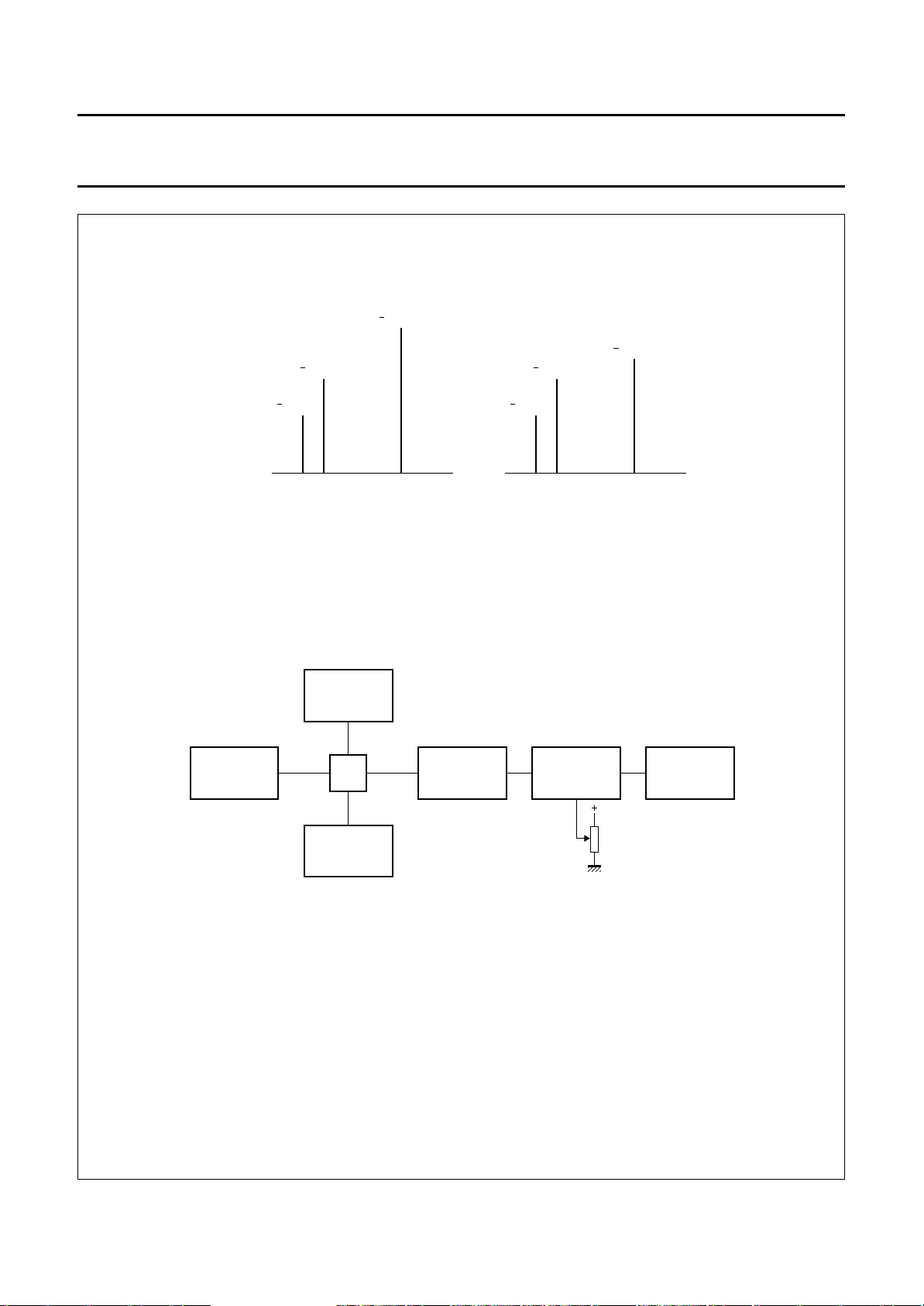
8. The test set-up and input conditions are given in Fig.12. The figures are measured with an input signal of
10 mV RMS.
9. Measured with a source impedance of 75 Ω, where:
− 4 − V
− 2 − V
− 3 − V
− 2 − V
− 200 −µA
S/N = 20 log
--------------------------------------------------------V
m rms()
10. To obtain a good noise immunity of the AGC circuit the AGC detector is gated during the sync pulse. This gating is
switched-off during the vertical retrace to avoid disturbances of the signal amplitude due to phase errors of the
incoming video signal which are caused by the head-switching of VCRs.
January 1995 29
V
(black-to-white)
O
B = 5 MHz()
Page 30

Philips Semiconductors Objective specification
I2C-bus controlled PAL/NTSC TV
TDA8366
processor
11. The AFC slope is directly related to the Q-factor of the demodulator tuned circuit. The given AFC steepness is
obtained with a Q-factor of 60. The AFC off-set is tested with a double sideband input signal and with the reference
tuned circuit tuned to minimum AGC voltage (optimum tuning for the demodulator).
2
The tuning information is supplied to the tuning system via the I
The first bit indicates whether the tuning is within the given window. The second bit indicates the direction of the
tuning. Bit indications:
a) AFA = 1; tuning inside window.
b) AFA = 0; tuning outside window.
c) AFB = 1; tuning too high.
d) AFB = 0; tuning too low.
To improve the speed of search tuning systems the AFC window can be increased to about 240 kHz. The width of
the window can be set by means of the AFW bit in subaddress 03.
12. Signal with negative-going sync. Amplitude includes sync pulse amplitude.
13. This parameter is measured at nominal settings of the various controls.
14. Indicated is a signal for a colour bar with 75% saturation (chroma : burst ratio = 2.2 : 1).
15. Nominal contrast is specified with the DAC in position 20H. Nominal saturation as maximum −10 dB. In the nominal
brightness setting the black level at the outputs is identical to the level of the black-current measuring pulses.
16. The −3 dB bandwidth of the circuit can be calculated by means of the following equation:
1
f
f
=
3dB–
17. Valid for a signal amplitude on the Y-input of 0.7 V black-to-white (100 IRE) with a rise time (10% to 90%) of 70 ns
and the video switch in the Y/C mode. During production the peaking function is not tested by measuring the
overshoots but by measuring the frequency response of the Y output.
18. The slicing level is independent of sync pulse amplitude. The given percentage is the distance between the slicing
level and the black level (back porch).
19. To obtain a good performance for both weak signal and VCR playback the time constant of the first control loop is
switched depending on the input signal condition and the condition of the I
noise detector and the time constant is switched to ‘slow’ when too much noise is present in the signal. In the ‘fast’
mode during the vertical retrace time the phase detector current is increased 50% so that phase errors due to
head-switching of the VCR are corrected as soon as possible. Switching between the two modes can be
automatically or overruled by the I2C-bus.
The circuit contains a video identification circuit which is independent of first loop. This identification circuit can be
used to close or open the first control loop when a video signal is present or not present on the input. This enables
a stable On Screen Display (OSD) when just noise is present at the input. The coupling of the video identification
circuit with the first loop can be defeated via the I2C-bus.
When the horizontal PLL is set to the ‘slow’ mode (via I2C-bus bits FOA and FOB) or during weak signal conditions
in the ‘automatic’ mode the phase detector is gated to obtain a good noise immunity. The width of the gating pulse
is 5.7 µs.
The output current of the phase detector in the various conditions are shown in Table 42.
20. During the start-up period of the oscillator the duty factor of the output pulse rises gradually from 0% to 50% (time
approximately 100 lines).
21. The start-up frequency depends on the SFM bit in the I2C-bus protocol. When SFM = 0 the frequency starts at a high
(non calibrated) value. When SFM = 1 the output signal will only be available after calibration.
1
–
osc
------- -
2Q
C-bus. Two bits have been reserved for this function.
2
C-bus. Therefore the circuit contains a
January 1995 30
Page 31

Philips Semiconductors Objective specification
I2C-bus controlled PAL/NTSC TV
TDA8366
processor
22. The timing pulses for the vertical ramp generator are obtained from the horizontal oscillator via a divider circuit. This
divider circuit has 3 modes of operation:
a) Search mode ‘large window’.
This mode is switched on when the circuit is not synchronized or when a non-standard signal (number of lines per
frame in the 50 Hz mode is between 311 and 314 and in the 60 Hz mode between 261 and 264). In the search mode
the divider can be triggered between line 244 and line 361 (approximately 45 to 64.5 Hz).
b) Standard mode ‘narrow window’.
This mode is switched on when more than 15 succeeding vertical sync pulses are detected in the narrow window.
When the circuit is in the standard mode and a vertical sync pulse is missing the retrace of the vertical ramp generator
is started at the end of the window. Consequently, the disturbance of the picture is very small. The circuit will switch
back to the search window when, for 6 successive vertical periods, no sync pulses are found within the window.
c) Standard TV-norm (divider ratio 525 (60 Hz) or 625 (50 Hz).
When the system is switched to the narrow window it is checked whether the incoming vertical sync pulses are in
accordance with the TV-norm. When 15 standard TV-norm pulses are counted the divider system is switched to the
standard divider ratio mode. In this mode the divider is always reset at the standard value even if the vertical sync
pulse is missing.
When 3 vertical sync pulses are missed the system switches back to the narrow window and when also in this
window no sync pulses are found (condition 3 missing pulses) the system switches over to the search window.
The vertical divider needs some waiting time during channel-switching of the tuner. When a fast reaction of the
divider is required during channel-switching the system can be forced to the search window by means of the NCIN bit
in subaddress 08.
23. Conditions: frequency is 50 Hz; normal mode; VS = 1F.
24. At a chrominance input voltage of 660 mV (p-p) (colour bar with 75% saturation i.e. burst signal amplitude
300 mV (p-p)) the dynamic range of the ACC is +6 and −20 dB.
25. All frequency variations are referenced to 3.58 or 4.43 MHz carrier frequency.
All oscillator specifications are measured with the Philips crystal series 9922 520.
If the spurious response of the 4.43 MHz crystal is lower than −1 dB with respect to the fundamental frequency for a
damping resistance of 1 kΩ, oscillation at the fundamental frequency is guaranteed.
The spurious response of the 3.58 MHz crystal must be lower than −1 dB with respect to the fundamental frequency
for a damping resistance of 1.5 kΩ.
The catching and detuning range are measured for nominal crystal parameters. These are:
a) Load resonance frequency f0= 4.433619 or 3.579545 MHz; CL= 20 pF.
b) Motional capacitance C1= 20.6 fF (4.43 MHz crystal) or 14.7 fF (3.58 MHz crystal).
c) Parallel capacitance C0= 5.5 pF (4.43 MHz crystal) or 4.5 pF (3.58 MHz crystal).
The actual load capacitance in the application should be CL= 18 pF to account for parasitic capacitances on and
off chip.
Philips Components has developed a special crystal which is tuned to the correct frequency in an application without
series capacitance (code number 9922 520 0038X; see Table 43). This has the advantage that the tuning (catching)
range is increased with approximately 50% without negative effects on spurious responses. When the catching range
of 300 Hz is considered too low this special crystal is a suitable alternative.
The free-running frequency of the oscillator can be checked by opening the colour PLL via the I2C-bus. In that
condition the colour killer is not active so that the frequency off-set is visible on the screen. When two crystals are
connected to the IC the circuit must be forced to one of the crystals during this test to prevent the oscillator switching
continuously between the two frequencies.
January 1995 31
Page 32
Philips Semiconductors Objective specification
I2C-bus controlled PAL/NTSC TV
TDA8366
processor
26. The (R−Y) and(B−Y) signals are demodulated with a phase difference of the reference carrier of 90° and a gain ratio
BY–()
-------------------- RY–()
27. This parameter indicates the bandwidth of the complete chrominance circuit including the chrominance bandpass
filter. The bandwidth of the low-pass filter of the demodulator is approximately 1 MHz.
28. At nominal setting of the gain control. When this amplitude is exceeded the peak-white limiting circuit will reduce the
contrast. The control voltage is generated via the external capacitor connected to the beam-current limiting input.
29. Signal-to-noise ratio (S/N) is specified as peak-to-peak signal with respect to RMS noise (bandwidth 5 MHz).
30. This is a current input. The indicated value of the nominal bias current is obtained at the nominal setting of the gain
(white point) control. The actual value of the bias current depends on the gain control setting of each channel. As a
result the ‘black-current’ of each gun is adapted to the white point setting so that the back-ground colour will follow
the white point adjustment.
Table 42 Output current of the phase detector in the various conditions
VID POC FOA FOB IDENT COIN NOISE SCAN V-RETR GATING MODE
− 0 0 0 yes yes yes 30 30 yes auto
− 0 0 0 yes no − 180 270 no auto
− 0 0 1 yes yes − 30 30 yes slow
− 0 0 1 yes no − 180 270 no slow
− 01−yes −−180 270 no fast
00−−no −−6 6 no OSD
− 1 −−−−−−−−off
1.78=
. The matrixing to the required signals is achieved in the control part.
2
C-BUS COMMANDS IC CONDITIONS ϕ-1 CURRENT/MODE
I
Table 43 Code numbers for special crystals
SYSTEM
PAL-N 3.582056 9922 520 00381
NTSC-M 3.579545 9922 520 00382
PAL-M 3.575611 9922 520 00383
PAL-B/G 4.433619 9922 520 00384
FREQUENCY
(MHz)
CODE NUMBER
January 1995 32
Page 33
Philips Semiconductors Objective specification
I2C-bus controlled PAL/NTSC TV
processor
50
(%)
30
10
10
30
50
048C10
DAC (HEX)
MLA738 - 1
F
50
(deg)
30
10
10
30
50
010203040
DAC (HEX)
TDA8366
MLA739 - 1
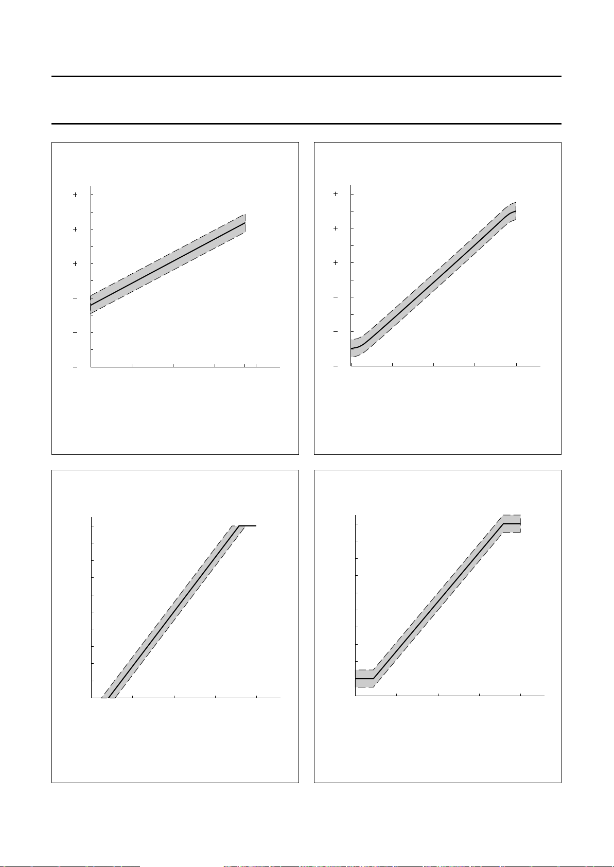
Overshoot in direction ‘black’.
Fig.5 Peaking control curve.
250
(%)
225
200
175
150
125
100
75
50
25
0
010203040
DAC (HEX)
MLA740 - 1
Fig.6 Hue control curve.
100
(%)
90
80
70
60
50
40
30
20
10
010203040
DAC (HEX)
MLA741 - 1
Fig.7 Saturation control curve. Fig.8 Contrast control curve.
January 1995 33
Page 34
Philips Semiconductors Objective specification
I2C-bus controlled PAL/NTSC TV
processor
MLA742 - 1
0.7
(V)
0.35
0
0.35
0.7
0
010203040
DAC (HEX)
MBC212
TDA8366
16 %
for negative modulation
100% = 10% rest carrier
100%
92%
30%
Relative variation with respect to the measuring pulse.
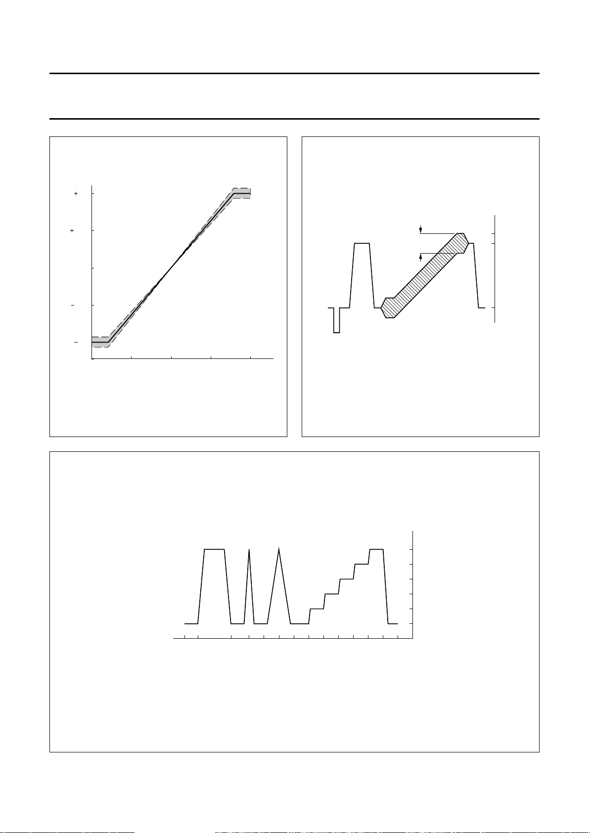
Fig.9 Brightness control curve.
MBC211
Fig.10 Video output signal.
100%
86%
72%
58%
44%
30%
µs
646056524844403632221210 26
January 1995 34
Fig.11 Test signal waveform.
Page 35
Philips Semiconductors Objective specification
I2C-bus controlled PAL/NTSC TV
processor
3.2 dB
13.2 dB
30 dB
SC CC PC
BLUE
13.2 dB
30 dB
SC CC PC
YELLOW
TDA8366
10 dB
MBC213
PC
SC Σ
CC
Input signal conditions: SC = sound carrier; CC = colour carrier; PC = picture carrier.
All amplitudes with respect to top sync level.
at 3.58 or 4.4 MHz
V
Value at 0.92 or 1.1 MHz 20 log
Value at 2.66 or 3.3 MHz 20 log
=
O
-----------------------------------------------------------at 0.92 or 1.1 MHz
V
O
at 3.58 or 4.4 MHz
V
O
------------------------------------------------------------
V
at 2.66 or 3.3 MHz
O
ATTENUATOR
3.6 dB+=
TEST
CIRCUIT
SPECTRUM
ANALYZER
gain setting
adjusted for blue
MBC210
January 1995 35
Fig.12 Test set-up intermodulation.
Page 36
Philips Semiconductors Objective specification
I2C-bus controlled PAL/NTSC TV
processor
TEST AND APPLICATION INFORMATION
handbook, full pagewidth
QSS IF
from
tuner
SAW
FILTER
IFDEM2
IFDEM1
2
4.4
MHz
2
1
47 and 46
33 3132
3.6
MHz
SOUND
TRAP
36
CVBS/
TXT
BAND
PASS
BAND
PASS
CVBS
EXT
SEC
CVBS/Y
CHROMA
TDA8366
28 27 30 29
RYO BYO BYI SCORYI
ref
STEREO AND CONTROL
RI GI BI RGBIN
21 22 23 24
658915411
37
L
R
SCL
SDA
RO
19
GO
18
BO
17
16 BLKIN
20 BCLIN
43
EWD
VDR
44
VDR
45
HOUT
38
39
to text decoder
TDA8366
(pos)
(neg)
FBI
TDA8395
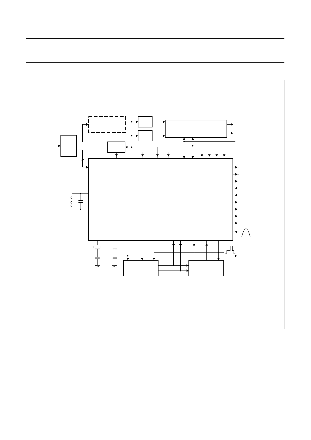
Fig.13 Application diagram.
East-West output stage
In order to obtain correct tracking of the vertical and
horizontal EHT-correction, the EW output stage should be
dimensioned as illustrated in Fig.14.
Resistor REW determines the gain of the EW output stage.
Resistor Rc determines the reference current for both the
vertical sawtooth generator and the geometry processor.
January 1995 36
TDA4661
The preferred value of R
is 39 kΩ which results in a
c
reference current of 100 µA (V
The value of R
EW
R
c
R
Example: With V
EW
V
×=
---------------------- 18 V
must be:
scan
×
ref
= 3.9 V; Rc=39kΩ and V
ref
then REW=68kΩ.
= 3.9 V).
ref
MLA746 - 1
scan
= 120 V
Page 37
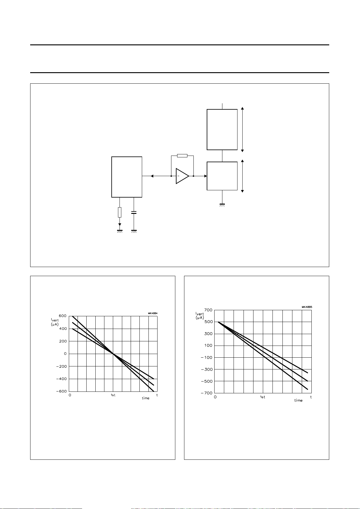
Philips Semiconductors Objective specification
I2C-bus controlled PAL/NTSC TV
processor
handbook, full pagewidth
TDA8366
43
EWD
4950
V
ref
R
39 kΩ
(2%)
I
c
ref
C
saw
100 nF
(5%)
R
ew
EW output
stage
V
DD
HORIZONTAL
DEFLECTION
STAGE
DIODE
MODULATOR
MLA744 - 1
V
V
TDA8366
scan
EW
Fig.14 East-West output stage.
VA = 0, 31H and 63H; VSH = 31H; SC = 0.
Fig.15 Control range of vertical amplitude.
January 1995 37
VS = 0, 31H and 63H; VA = 31H; VHS = 31H; SC = 0.
Fig.16 Control range of vertical slope.
Page 38
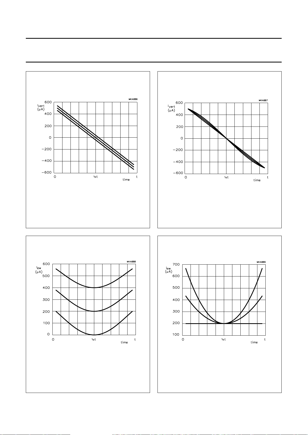
Philips Semiconductors Objective specification
I2C-bus controlled PAL/NTSC TV
processor
TDA8366
VSH = 0, 31H and 63H; VA = 31H; SC = 0.
Fig.17 Control range of vertical shift.
SC = 0, 31H and 63H; VA = 31H; VHS = 31H.
Fig.18 Control range of S-correction.
EW = 0, 31H and 63H; PW = 31H; CP = 31H.
Fig.19 Control range of EW width.
January 1995 38
PW = 0, 31H and 63H; EW = 31H; CP = 31H.
Fig.20 Control range of EW parabola/width ratio.
Page 39
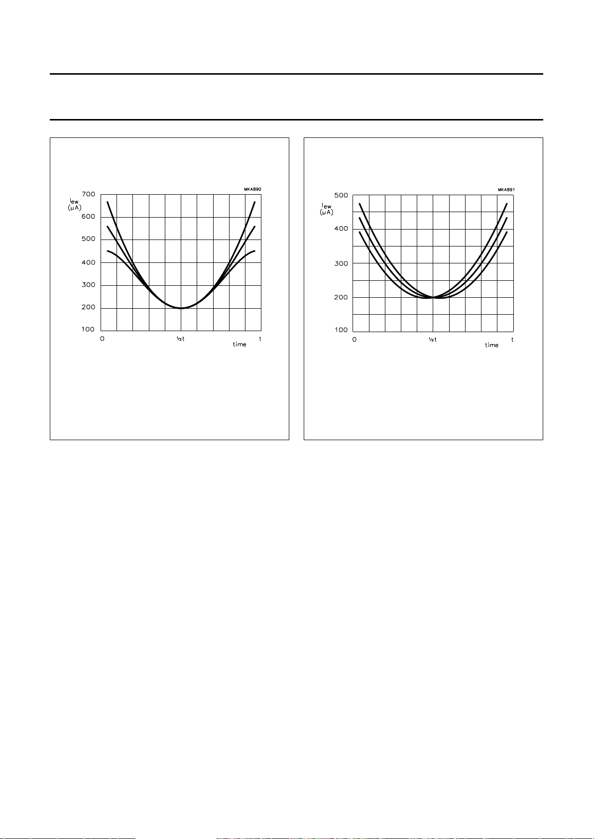
Philips Semiconductors Objective specification
I2C-bus controlled PAL/NTSC TV
processor
TDA8366
CP = 0, 31H and 63H; EW = 31H; PW = 63H.
Fig.21 Control range of EW corner/parabola ratio.
TC = 0, 31H and 63H; EW = 31H; PW = 31H.
Fig.22 Control range of EW trapezium correction.
January 1995 39
Page 40

Philips Semiconductors Objective specification
I2C-bus controlled PAL/NTSC TV
processor
Adjustment of geometry control parameters
The deflection processor of the TDA8366 offers nine
control parameters for picture alignment:
• Vertical picture alignment
– S-correction
– vertical amplitude
– vertical slope
– vertical shift
• Horizontal picture alignment
– horizontal shift
– EW width
– EW parabola/width
– EW corner/parabola
– EW trapezium correction.
It is important to notice that the TDA8366 is designed for
use with a DC-coupled vertical deflection stage. This is the
reason why a vertical linearity alignment is not necessary
(and therefore not available).
For a particular combination of picture tube type, vertical
output stage and EW output stage it is determined which
are the required values for the settings of S-correction, EW
parabola/width ratio and EW corner/parabola ratio. These
parameters can be preset via the I
any additional adjustment. The rest of the parameters are
preset with the mid-value of their control range (i.e. 1FH),
or with the values obtained by previous TV-set
adjustments.
The vertical shift control is meant for compensation of
off-sets in the external vertical output stage or in the
picture tube. It can be shown that without compensation
these off-sets will result in a certain linearity error,
especially with picture tubes that need large S-correction.
The total linearity error is in first order approximation
proportional to the value of the off-set, and to the square of
the S-correction needed. The necessity to use the vertical
shift alignment depends on the expected off-sets in vertical
output stage and picture tube, on the required value of the
S-correction, and on the demands upon vertical linearity.
2
C-bus, and do not need
TDA8366
For adjustment of the vertical shift and vertical slope
independent of each other, a special service blanking
mode can be entered by setting the SBL bit HIGH. In this
mode the RGB-outputs are blanked during the second half
of the picture. There are 2 different methods for alignment
of the picture in vertical direction. Both methods make use
of the service blanking mode.
The first method is recommended for picture tubes that
have a marking for the middle of the screen. With the
vertical shift control the last line of the visible picture is
positioned exactly in the middle of the screen. After this
adjustment the vertical shift should not be changed. The
top of the picture is placed by adjustment of the vertical
amplitude, and the bottom by adjustment of the vertical
slope.
The second method is recommended for picture tubes that
have no marking for the middle of the screen. For this
method a video signal is required in which the middle of the
picture is indicated (e.g. the white line in the circle test
pattern). With the vertical slope control the beginning of the
blanking is positioned exactly on the middle of the picture.
Then the top and bottom of the picture are placed
symmetrical with respect to the middle of the screen by
adjustment of the vertical amplitude and vertical shift.
After this adjustment the vertical shift has the right setting
and should not be changed.
If the vertical shift alignment is not required VSH should be
set to its mid-value (i.e. VSH = 1F). Then the top of the
picture is placed by adjustment of the vertical amplitude
and the bottom by adjustment of the vertical slope. After
the vertical picture alignment the picture is positioned in
the horizontal direction by adjustment of the EW width and
the horizontal shift. Finally (if necessary) the left- and
right-hand sides of the picture are aligned in parallel by
adjusting the EW trapezium control.
After adjustment of the picture for normal vertical
deflection as described, no additional adjustment is
necessary for the compress and expand mode. If required
a small correction of the picture height can be made by
adjusting the vertical slope. This will not effect the linearity.
January 1995 40
Page 41
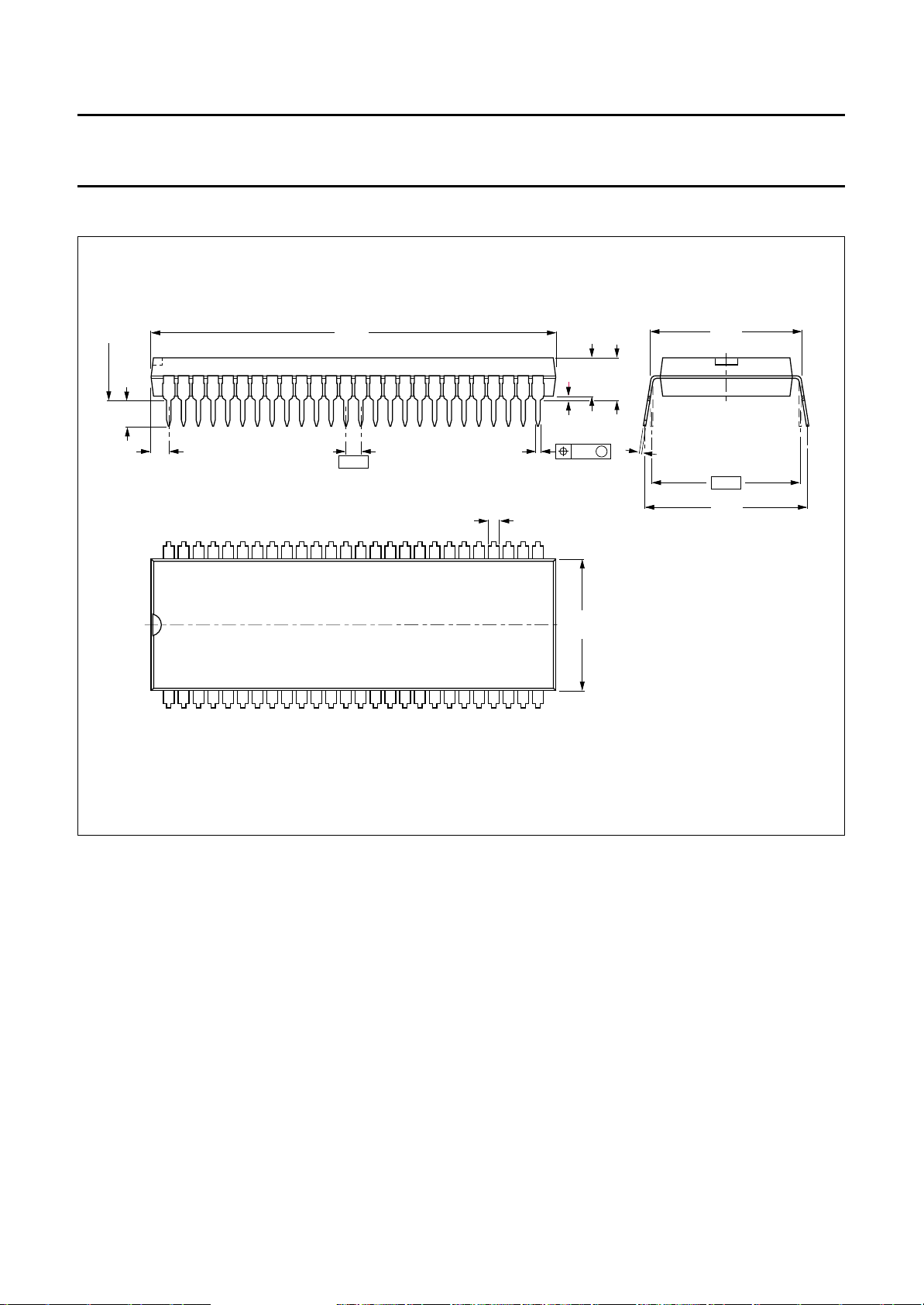
Philips Semiconductors Objective specification
I2C-bus controlled PAL/NTSC TV
processor
PACKAGE OUTLINES
handbook, full pagewidth
seating plane
3.2
2.8
1.73
max
52
47.92
47.02
1.778
(25x)
1.3 max
0.53
max
27
0.51
min
4.57
max
0.18 M
TDA8366
15.80
15.24
5.08
max
0.32 max
15.24
17.15
15.90
MSA267
1
Dimensions in mm.
14.1
13.7
26
Fig.23 Plastic shrink dual in-line package; 52 leads (600 mil) SDIP52; SOT247-1.
January 1995 41
Page 42
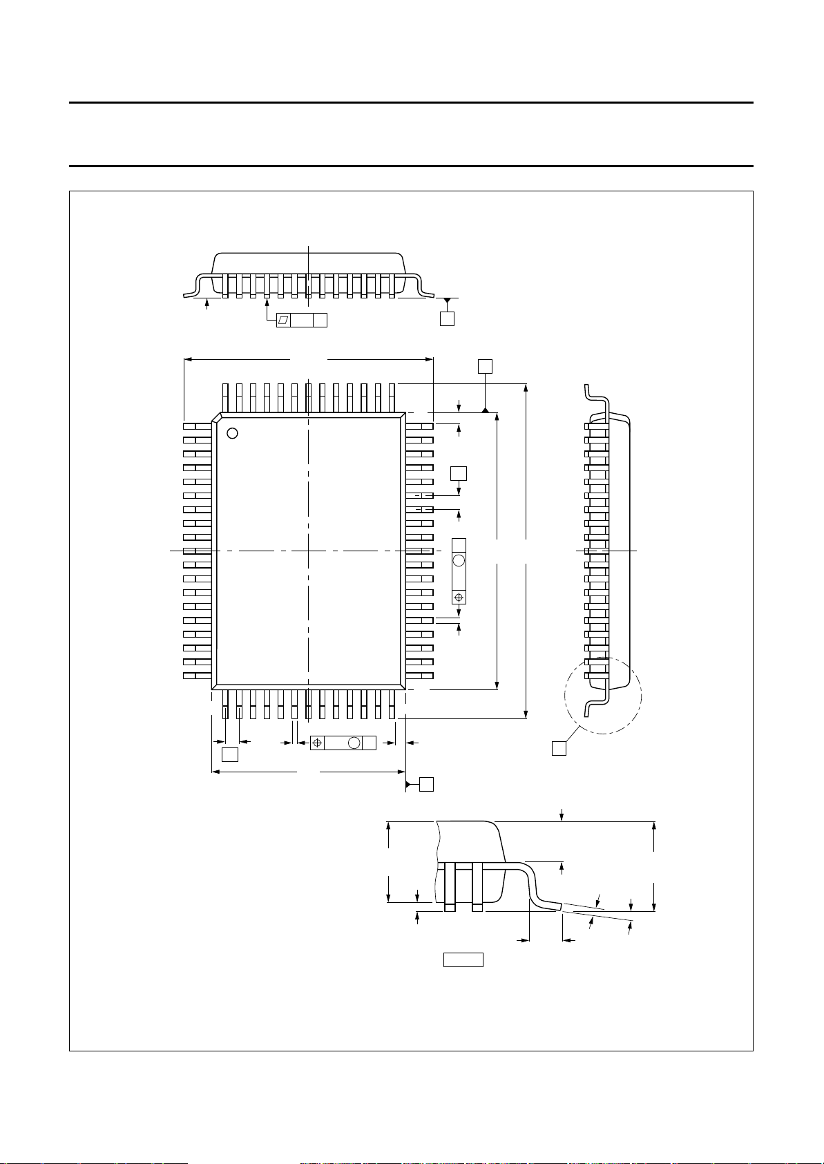
Philips Semiconductors Objective specification
I2C-bus controlled PAL/NTSC TV
processor
handbook, full pagewidth
seating plane
64 52
1
pin 1 index
0.10
18.2
17.6
S
TDA8366
S
B
51
1.2
(4x)
0.8
1.0
B
20.1
24.2
19.9
23.6
0.20 M
0.50
0.35
2.90
2.65
33
3220
1.2
0.25
0.05
0.8
A
(4x)
detail X
1.0
0.6
X
1.4
1.2
0.25
0.14
0 to 7
MSA327
3.2
2.7
o
19
1.0
0.50
0.35
0.20 M A
14.1
13.9
Dimensions in mm.
Fig.24 Plastic quad flat package; 64 leads (lead length 1.95 mm); body 14 × 20 × 2.8 mm.
January 1995 42
Page 43

Philips Semiconductors Objective specification
I2C-bus controlled PAL/NTSC TV
processor
SOLDERING
Plastic dual in-line packages
Y DIP OR WAVE
B
The maximum permissible temperature of the solder is
260 °C; this temperature must not be in contact with the
joint for more than 5 s. The total contact time of successive
solder waves must not exceed 5 s.
The device may be mounted up to the seating plane, but
the temperature of the plastic body must not exceed the
specified storage maximum. If the printed-circuit board has
been pre-heated, forced cooling may be necessary
immediately after soldering to keep the temperature within
the permissible limit.
EPAIRING SOLDERED JOINTS
R
Apply a low voltage soldering iron below the seating plane
(or not more than 2 mm above it). If its temperature is
below 300 °C, it must not be in contact for more than 10 s;
if between 300 and 400 °C, for not more than 5 s.
Plastic quad flat-packs
YWAVE
B
During placement and before soldering, the component
must be fixed with a droplet of adhesive. After curing the
adhesive, the component can be soldered. The adhesive
can be applied by screen printing, pin transfer or syringe
dispensing.
Maximum permissible solder temperature is 260 °C, and
maximum duration of package immersion in solder bath is
10 s, if allowed to cool to less than 150 °C within 6 s.
Typical dwell time is 4 s at 250 °C.
TDA8366
A modified wave soldering technique is recommended
using two solder waves (dual-wave), in which a turbulent
wave with high upward pressure is followed by a smooth
laminar wave. Using a mildly-activated flux eliminates the
need for removal of corrosive residues in most
applications.
Y SOLDER PASTE REFLOW
B
Reflow soldering requires the solder paste (a suspension
of fine solder particles, flux and binding agent) to be
applied to the substrate by screen printing, stencilling or
pressure-syringe dispensing before device placement.
Several techniques exist for reflowing; for example,
thermal conduction by heated belt, infrared, and
vapour-phase reflow. Dwell times vary between 50 and
300 s according to method. Typical reflow temperatures
range from 215 to 250 °C.
Preheating is necessary to dry the paste and evaporate
the binding agent. Preheating duration: 45 min at 45 °C.
EPAIRING SOLDERED JOINTS (BY HAND-HELD SOLDERING
R
IRON OR PULSE
Fix the component by first soldering two, diagonally
opposite, end pins. Apply the heating tool to the flat part of
the pin only. Contact time must be limited to 10 s at up to
300 °C. When using proper tools, all other pins can be
soldered in one operation within 2 to 5 s at between 270
and 320 °C. (Pulse-heated soldering is not recommended
for SO packages.)
For pulse-heated solder tool (resistance) soldering of VSO
packages, solder is applied to the substrate by dipping or
by an extra thick tin/lead plating before package
placement.
-HEATED SOLDER TOOL)
January 1995 43
Page 44

Philips Semiconductors Objective specification
I2C-bus controlled PAL/NTSC TV
TDA8366
processor
DEFINITIONS
Data sheet status
Objective specification This data sheet contains target or goal specifications for product development.
Preliminary specification This data sheet contains preliminary data; supplementary data may be published later.
Product specification This data sheet contains final product specifications.
Limiting values
Limiting values given are in accordance with the Absolute Maximum Rating System (IEC 134). Stress above one or
more of the limiting values may cause permanent damage to the device. These are stress ratings only and operation
of the device at these or at any other conditions above those given in the Characteristics sections of the specification
is not implied. Exposure to limiting values for extended periods may affect device reliability.
Application information
Where application information is given, it is advisory and does not form part of the specification.
LIFE SUPPORT APPLICATIONS
These products are not designed for use in life support appliances, devices, or systems where malfunction of these
products can reasonably be expected to result in personal injury. Philips customers using or selling these products for
use in such applications do so at their own risk and agree to fully indemnify Philips for any damages resulting from such
improper use or sale.
PURCHASE OF PHILIPS I
Purchase of Philips I
components in the I2C system provided the system conforms to the I2C specification defined by
Philips. This specification can be ordered using the code 9398 393 40011.
2
C COMPONENTS
2
C components conveys a license under the Philips’ I2C patent to use the
January 1995 44
 Loading...