

Page 1

INTEGRATED CIRCUITS
DATA SH EET
TDA8351A
DC-coupled vertical deflection
output circuit
Objective specification
File under Integrated Circuits, IC02
Philips Semiconductors
January 1995
Page 2

Philips Semiconductors Objective specification
DC-coupled vertical deflection
TDA8351A
output circuit
FEATURES
• Few external components
• Highly efficient fully DC-coupled vertical output bridge
circuit
• Vertical flyback switch
• Guard circuit
• Protection against:
– short-circuit of the output pins (9 and 5)
– short-circuit of the output pins to V
P
• Temperature (thermal) protection
• High EMC immunity because of common mode inputs
• A guard signal in zoom mode.
QUICK REFERENCE DATA
SYMBOL PARAMETER CONDITIONS MIN. TYP. MAX. UNIT
DC supply
V
P
I
q
supply voltage 9 16 25 V
quiescent supply current − 30 − mA
Vertical circuit
I
O(p-p)
output current
(peak-to-peak value)
I
diff(p-p)
differential input current
(peak-to-peak value)
V
diff(p-p)
differential input voltage
(peak-to-peak value)
GENERAL DESCRIPTION
The TDA8351A is a power circuit for use in 90° and 110°
colour deflection systems for field frequencies of 50 to
120 Hz. The circuit provides a DC driven vertical deflection
output circuit, operating as a highly efficient class G
system.
−−3A
− 600 −µA
− 1.8 − V
Flyback switch
I
M
V
FB
peak output current t ≤ 1.5 ms −−±1.5 A
flyback supply voltage −−50 V
note 1 −−60 V
Thermal data (in accordance with IEC 747-1)
T
stg
T
amb
T
vj
storage temperature −55 − +150 °C
operating ambient temperature −25 − +75 °C
virtual junction −−150 °C
Note
1. A flyback supply voltage of>50 V up to 60 V is allowed in application. A 220 nF capacitor in series with a 22 Ω resistor
(dependent on I
and the inductance of the coil) has to be connected between pin 7 and ground. The decoupling
O
capacitor of VFB has to be connected between pin 9 and pin 5. This supply voltage line must have a resistance of
33 Ω (see application circuit Fig.5).
January 1995 2
Page 3
Philips Semiconductors Objective specification
DC-coupled vertical deflection
TDA8351A
output circuit
ORDERING INFORMATION
SOURCE
PACKAGE
V
FB
TYPE NUMBER
NAME DESCRIPTION VERSION
TDA8351A DBS13P plastic DIL-bent-SIL power package; 13 leads (lead length 12 mm) SOT141-6
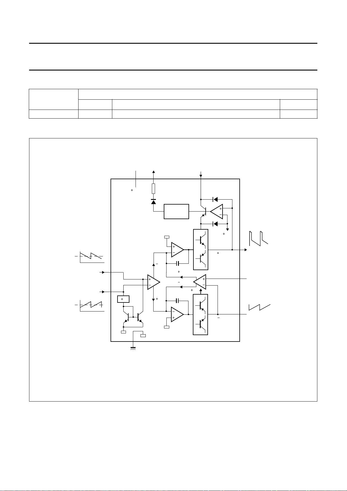
BLOCK DIAGRAM
V
V
O(guard)
handbook, full pagewidth
P
48
V
P
10
CURRENT
TDA8351A
I
drive(pos)
I
drive(neg)
1
2
V
7
GND
I
S
I
T
I
T
V
I
S
Fig.1 Block diagram.
V
P
9
V
V
O(A)
P
V
O(B)
MGC055
O(A)
3
V
I(fb)
5
V
O(B)
January 1995 3
Page 4
Philips Semiconductors Objective specification
DC-coupled vertical deflection
output circuit
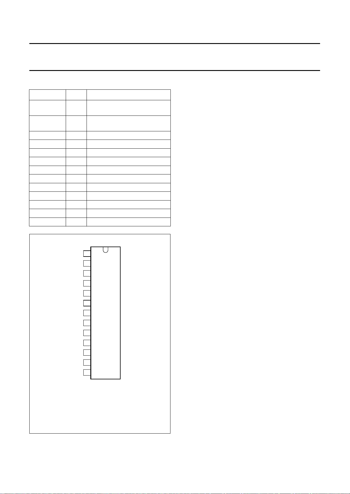
PINNING
SYMBOL PIN DESCRIPTION
I
drive(pos)
I
drive(neg)
V
I(fb)
V
P
V
O(B)
n.c. 6 not connected
GND 7 ground
V
FB
V
O(A)
V
O(guard)
n.c. 11 not connected
n.c. 12 not connected
n.c. 13 not connected
handbook, halfpage
1 input power-stage (positive);
includes I
signal bias
I(sb)
2 input power-stage (negative);
includes I
signal bias
I(sb)
3 input feedback voltage
4 supply voltage
5 output voltage B
8 input flyback supply voltage
9 output voltage A
10 guard output voltage
I
drive(pos)
I
drive(neg)
V
O(guard)
V
V
V
I(fb)
V
O(B)
n.c.
GND
V
FB
O(A)
n.c.
n.c.
n.c.
p
1
2
3
4
5
6
7
TDA8351A
8
9
10
11
12
13
MGC056
TDA8351A
FUNCTIONAL DESCRIPTION
The vertical driver circuit is a bridge configuration. The
deflection coil is connected between the output amplifiers,
which are driven in phase opposition. An external resistor
(RM) connected in series with the deflection coil provides
internal feedback information. The differential input circuit
is voltage driven. The input circuit has been adapted to
enable it to be used with the TDA9150, TDA9151B,
TDA9160A, TDA9162, TDA8366 and TDA8367 which
deliver symmetrical current signals. An external resistor
) connected between the differential input
(R
CON
determines the output current through the deflection coil.
The relationship between the differential input current and
the output current is defined by: I
The output current is adjustable from 0.5 A (p-p) to 3 A
(p-p) by varying RM. The maximum input differential
voltage is 1.8 V. In the application it is recommended that
V
= 1.5 V (typ). This is recommended because of the
diff
spread of input current and the spread in the value of
R
.
CON
The flyback voltage is determined by an additional supply
voltage VFB. The principle of operating with two supply
voltages (class G) makes it possible to fix the supply
voltage VP optimum for the scan voltage and the second
supply voltage VFB optimum for the flyback voltage. Using
this method, very high efficiency is achieved.
The supply voltage VFB is almost totally available as
flyback voltage across the coil, this being possible due to
the absence of a decoupling capacitor (not necessary, due
to the bridge configuration). The output circuit is fully
protected against the following:
• thermal protection
• short-circuit protection of the output pins (pins 5 and 9)
• short-circuit of the output pins to VP.
A guard circuit V
is provided. The guard circuit is
O(guard)
activated at the following conditions:
• during flyback
• during short-circuit of the coil and during short-circuit of
the output pins (pins 5 and 9) to VP or ground
• during open loop
• when the thermal protection is activated.
diff
× R
CON=Icoil
× RM.
The die has been glued to the metal block of the package. If the metal
block is not insulated from the heat sink, the heat sink may only be
connected directly to pin 7.
Fig.2 Pin configuration.
January 1995 4
This signal can be used for blanking the picture tube
screen.
Page 5
Philips Semiconductors Objective specification
DC-coupled vertical deflection
TDA8351A
output circuit
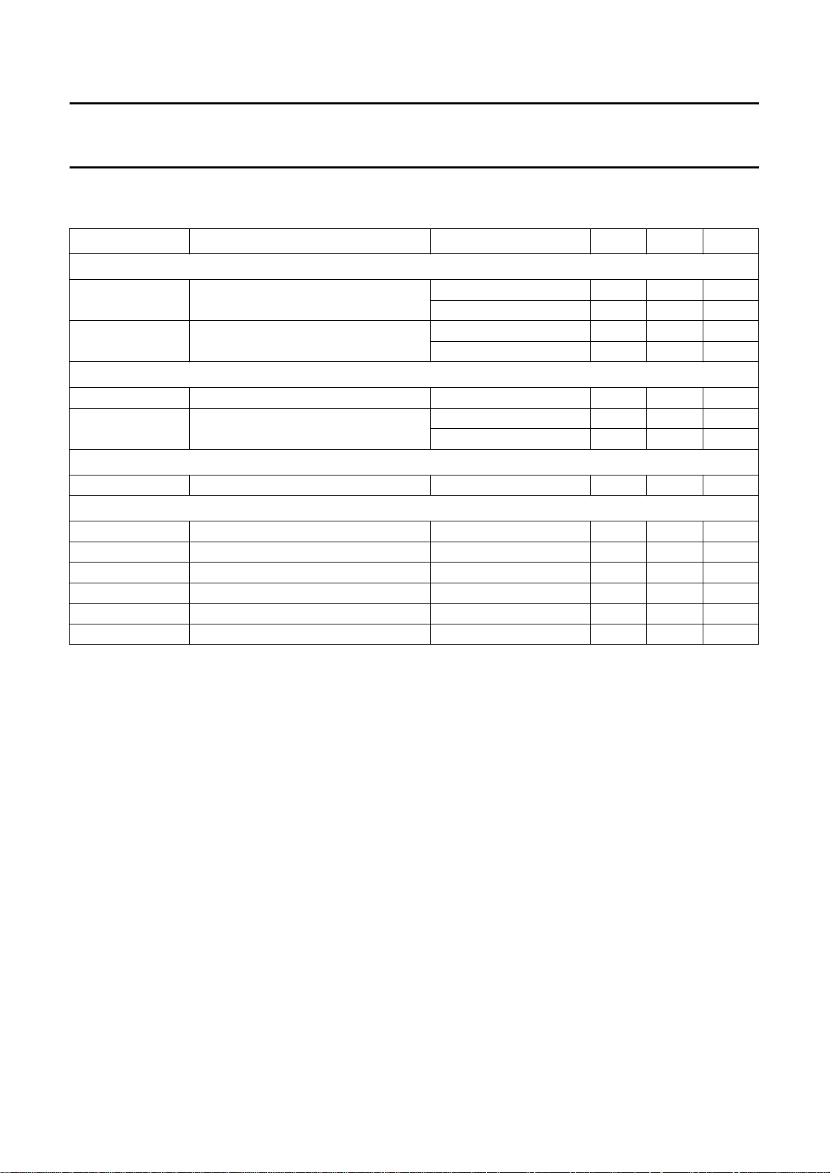
LIMITING VALUES
In accordance with the Absolute Maximum Rating System (IEC 134).
SYMBOL PARAMETER CONDITIONS MIN. MAX. UNIT
DC supply
V
P
V
FB
Vertical circuit
I
O(p-p)
V
O(A)
Flyback switch
I
M
Thermal data (in accordance with IEC 747-1)
T
stg
T
amb
T
vj
R
th vj-c
R
th vj-a
t
sc
supply voltage non-operating − 40 V
− 25 V
flyback supply voltage − 50 V
note 1 − 60 V
output current (peak-to-peak value) note 2 − 3A
output voltage (pin 7) − 52 V
note 1 − 62 V
peak output current −±1.5 A
storage temperature −55 +150 °C
operating ambient temperature −25 +75 °C
virtual junction temperature − 150 °C
resistance vj-case − 4 K/W
resistance vj-ambient in free air − 40 K/W
short-circuiting time note 3 − 1hr
Notes
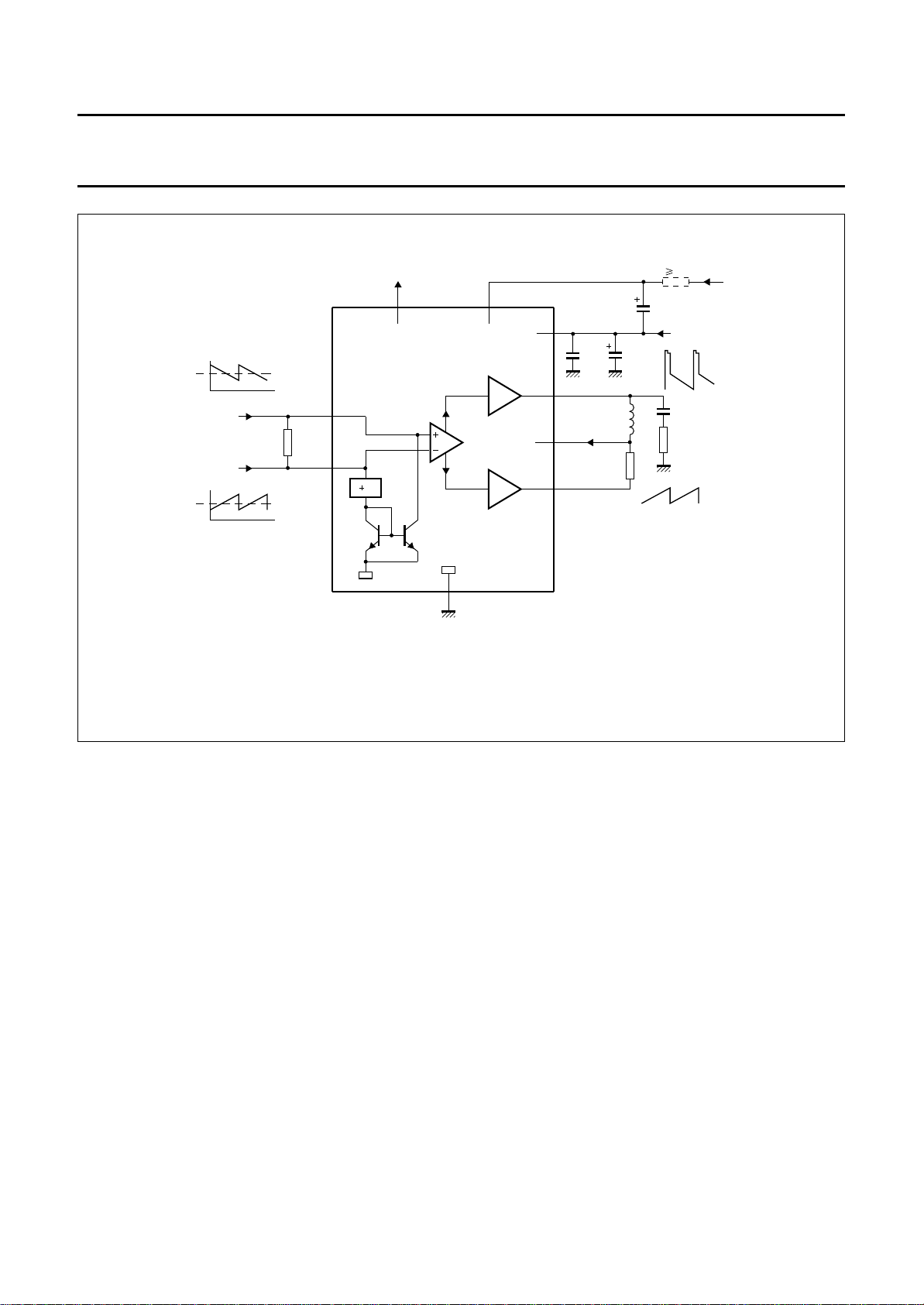
1. A flyback supply voltage of>50 V up to 60 V is allowed in application. A 220 nF capacitor in series with a 22 Ω resistor
(dependent on I
and the inductance of the coil) has to be connected between pin 7 and ground. The decoupling
O
capacitor of VFB has to be connected between pin 6 and pin 3. This supply voltage line must have a resistance of
33 Ω (see application circuit Fig.5).
2. IO maximum determined by current protection.
3. Up to VP=18V.
January 1995 5
Page 6
Philips Semiconductors Objective specification
DC-coupled vertical deflection
TDA8351A
output circuit
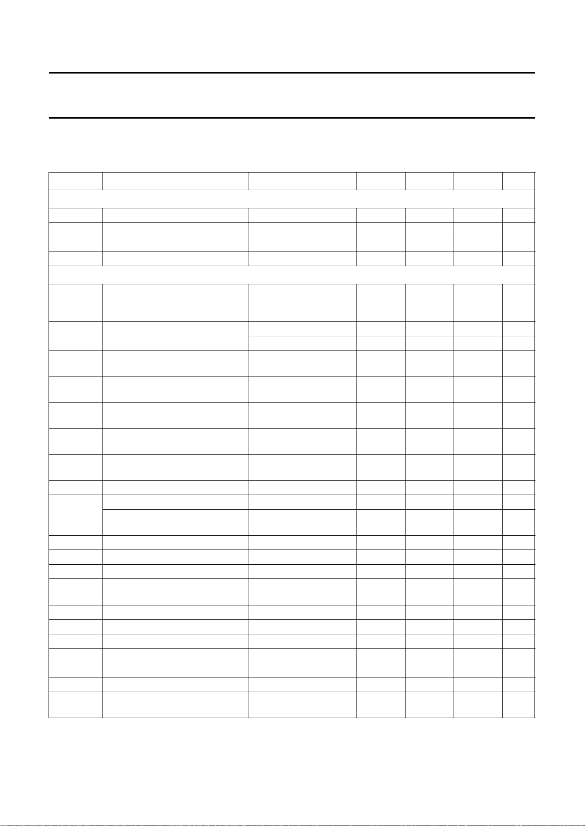
CHARACTERISTICS
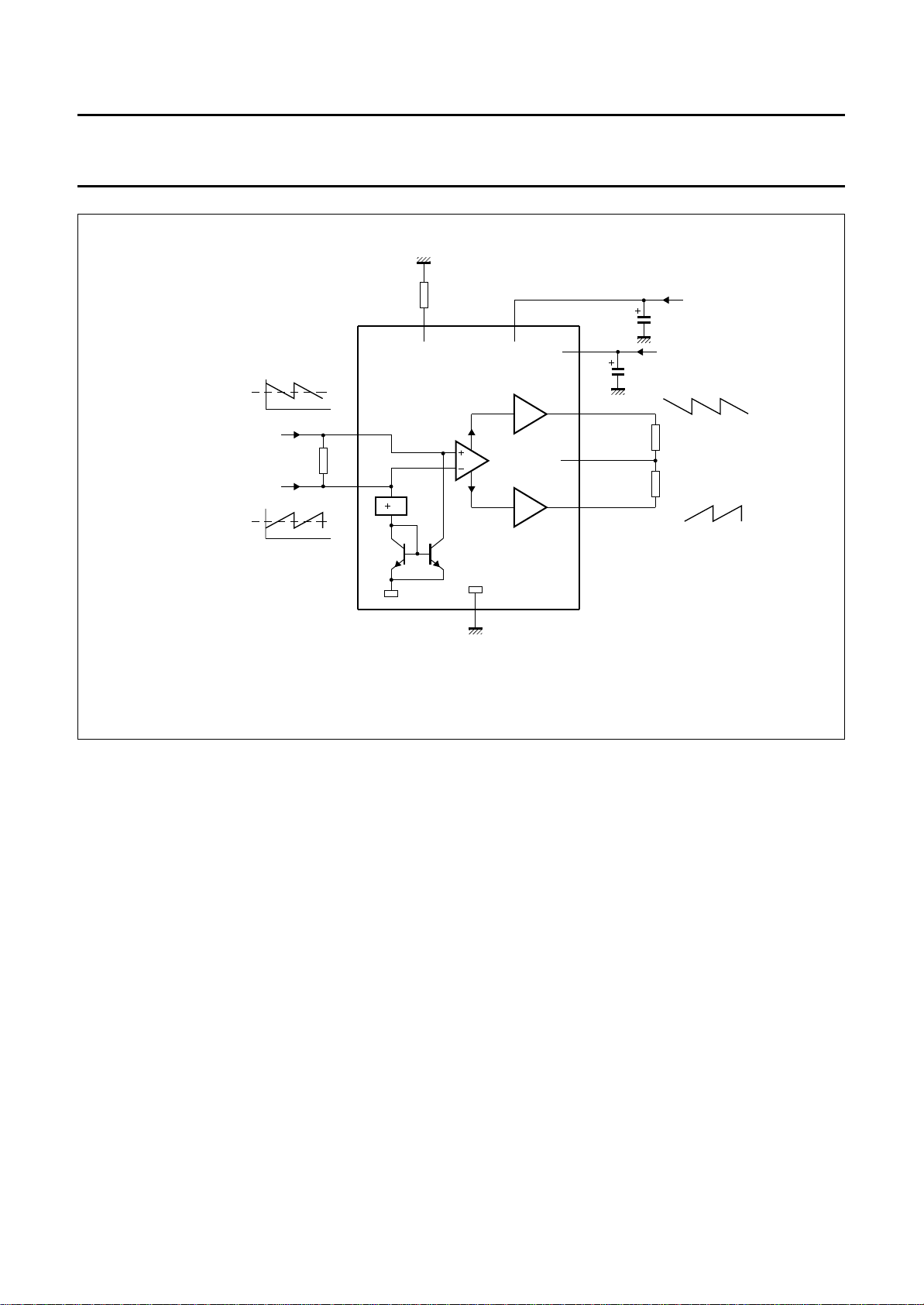
VP= 17.5 V; VFB= 45 V; fi= 50 Hz; I
specified.
SYMBOL PARAMETER CONDITIONS MIN. TYP. MAX. UNIT
DC supply
V
P
V
FB
I
P
operating supply voltage 9.0 − 25 V
flyback supply voltage V
supply current no signal; no load − 30 55 mA
Vertical circuit
V
O
output voltage swing (scan) I
LE linearity error I
V
O
V
DF
| output offset current I
|I
os
|V
| offset voltage at the input of the
os
output voltage swing (flyback)
V
O(A)-VO(B)
forward voltage of the internal
efficiency diode (V
O(A)-VFB
feedback amplifier (V
T output offset voltage as a function
∆V
os
of temperature
V
G
O(A)
vo
DC output voltage I
open-loop voltage gain (V
open loop voltage gain
; V
(V
7-4/V9-4
V
R
f
res
G
I
T current gain drift as a function of
∆G
c
voltage ratio V
frequency response (−3 dB) open loop; note 6 − 40 − Hz
current gain (IO/I
=0)
1-2
1-2/V9-4
) − 5000 −
diff
temperature
I
I(sb)
I
FB
signal bias current 50 400 500 µA
flyback supply current during scan −−100 µA
PSRR power supply ripple rejection note 7 − 80 − dB
V
I(DC)
V
I(CM)
I
bias
I
O(CM)
DC input voltage − 2.7 − V
common mode input voltage I
input bias current I
common mode output current ∆I
= 400 µA; T
I(sb)
)
I(fb)-VO(B)
7-4/V1-2
=25°C; measured in test circuit of Fig.3; unless otherwise
amb
− 50 V
− 60 V
note 1 V
= 0.6 mA (p-p);
diff
V
= 1.8 V (p-p);
diff
P
P
19.8 −−V
IO= 3 A (p-p)
= 3 A (p-p); note 2 − 12%
O
= 50 mA (p-p); note 2 − 12%
I
O
I
= 0.3 mA;
diff
− 39 − V
IO= 1.5 A (M)
IO= −1.5 A (M);
I
= 0.3 mA
diff
=0;
diff
I
=50to500µA
I(sb)
I
=0;
diff
)
I
=50to500µA
I(sb)
I
=0 −−72 µV/K
diff
= 0; note 3 − 8.0 − V
diff
−−1.5 V
−−30 mA
−−18 mV
) notes 4 and 5 − 80 − dB
note 4 − 80 − dB
− 0 − dB
−−10
=0 0 − 1.6 V
I(sb)
=0 − 0.1 0.5 µA
I(sb)
= 300 µA (p-p);
I(sb)
fi= 50 Hz; I
diff
=0
− 0.2 − mA
−4
K
January 1995 6
Page 7

Philips Semiconductors Objective specification
DC-coupled vertical deflection
TDA8351A
output circuit
SYMBOL PARAMETER CONDITIONS MIN. TYP. MAX. UNIT
Guard circuit
I
O
V
O(guard)
output current not active;
V
O(guard)
active; V
=0V
O(guard)
= 4.5 V 1 − 2.5 mA
output voltage on pin 8 IO= 100 µA −−5.5 V
allowable voltage on pin 8 maximum leakage
current = 10 µA;
Notes
1. A flyback supply voltage of>50 V up to 60 V is allowed in application. A 220 nF capacitor in series with a 22 Ω resistor
(dependent on I
and the inductance of the coil) has to be connected between pin 7 and ground. The decoupling
O
capacitor of VFB has to be connected between pin 9 and pin 5. This supply voltage line must have a resistance of
33 Ω (see application circuit Fig.5).
2. The linearity error is measured without S-correction and based on the same measurement principle as performed on
the screen. The measuring method is as follows:
Divide the output signal I
5-I9(VRM
) into 22 equal parts ranging from 1 to 22 inclusive. Measure the value of two
succeeding parts called one block starting with part 2 and 3 (block 1) and ending with part 20 and 21 (block 10). Thus
part 1 and 22 are unused. The equations for linearity error for adjacent blocks (LEAB) and not adjacent blocks (NAB)
are given below
a
–
kak1+()
LEAB
= NAB
----------------------------- a
3. Referenced to V
avg
;
.
P
a
maxamin
=
----------------------------- a
–
avg
4. V values within formulae, relate to voltages at or between relative pin numbers, i.e. V
pins 7 and 4 divided by voltage value across pins 1 and 2.
5. V
6. Frequency response V
7. At V
AC short-circuited.
9-4
= 500 mV eff; measured across RM; fi= 50 Hz.
(ripple)
is equal to frequency response V
9-5/V3-5
9-5/V1-2
−−50 µA
−−40 V
9-5/V1-2
= voltage value across
.
January 1995 7
Page 8
Philips Semiconductors Objective specification
DC-coupled vertical deflection
output circuit
handbook, full pagewidth
V
I
I(sb)
signal
bias
I
drive(pos)
I
drive(neg)
signal
bias
I
I(sb)
R
CON
3 kΩ
1
I
diff
2
O(guard)
TDA8351A
V
2.2 kΩ
10 8
FEEDBACK
INPUT
TDA8351A
V
FB
4
9
3
5
V
P
R = 6.0 Ω
R = 0.7 Ω
M
7
GND
Fig.3 Test diagram.
MGC057
January 1995 8
Page 9
Philips Semiconductors Objective specification
DC-coupled vertical deflection
output circuit
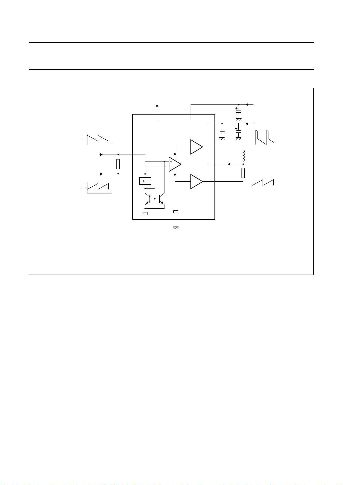
APPLICATION INFORMATION
handbook, full pagewidth
I
I(sb)
signal
bias
I
drive(pos)
R
CON
I
diff
I
drive(neg)
signal
bias
I
I(sb)
3 kΩ
V
O(guard)
1
2
10 8
TDA8351A
V
FEEDBACK
7
GND
INPUT
MGC058
TDA8351A
V
FB
4
100
nF
V
O(A)
9
I
(coil)
V
I(fb)
3
V
O(B)
5
V
P
deflection coil
AT6005/31
L = 8.63 mH
R = 5.0 Ω
R = 0.7 Ω
M
VP= 14 V; I
O(p-p)
= 2.14 A; I
= 400 µA; I
I(sb)
= 500 µA; VFB= 42 V; tFB= 0.6 ms.
diff(p-p)
Fig.4 Application diagram.
January 1995 9
Page 10
Philips Semiconductors Objective specification
DC-coupled vertical deflection
output circuit
handbook, full pagewidth
V
O(guard)
I
I(sb)
signal
bias
1
I
diff
2
signal
bias
I
I(sb)
I
drive(pos)
I
drive(neg)
R
CON
3 kΩ
10 8
TDA8351A
V
FEEDBACK
7
GND
INPUT
4
9
3
5
MGC059
100
nF
V
O(A)
V
I(fb)
R = 0.7 Ω
M
V
O(B)
I
(coil)
30
V
P
470 nF
20 Ω
TDA8351A
V
FB
deflection coil
AT6005/31
L = 8.63 mH
R = 5.0 Ω
VP= 14 V; I
O(p-p)
= 2.14 A; I
= 400 µA; I
I(sb)
= 500 µA; VFB= 60 V; tFB= 0.4 ms.
diff(p-p)
Fig.5 Application circuit; 50 V ≤ VFB≤ 60 V.
January 1995 10
Page 11
Philips Semiconductors Objective specification
DC-coupled vertical deflection
output circuit
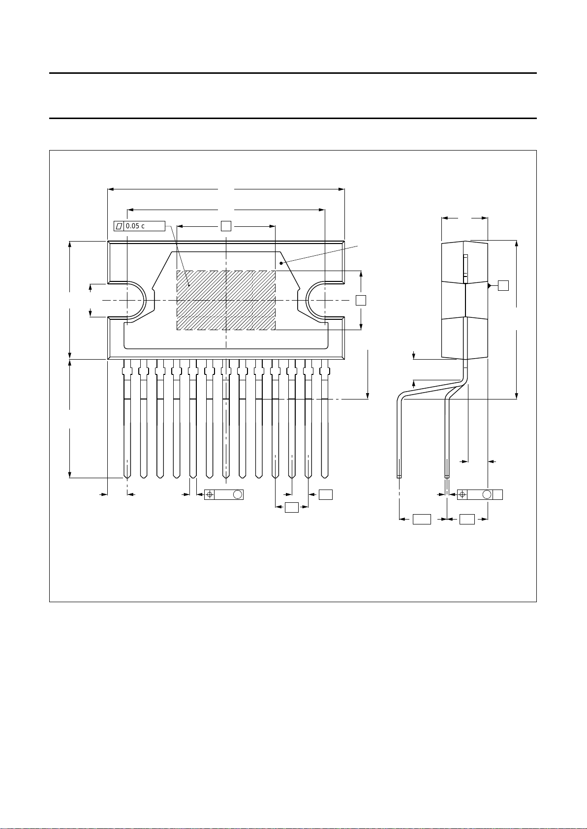
PACKAGE OUTLINE
handbook, full pagewidth
0.05 convex
3.4
12.4
3.1
11.6
987654321
10111213
24.4
23.6
20.0
19.6
10
mounting
base
6
seating plane
2.4
1.6
TDA8351A
4.7
4.1
A
17.0
15.5
13
11
2.20
1.45
Dimensions in mm.
Fig.6 Plastic DIL-bent-SIL power package; 13leads (lead length 12 mm); DBS13P; SOT141-6.
0.75
0.60
0.25
(13x)
2.1
1.8
M
3.4
1.7
(12x)
0.55
0.35
4.35.08
0.8
(13x)
M
A
MBC369
January 1995 11
Page 12

Philips Semiconductors Objective specification
DC-coupled vertical deflection
TDA8351A
output circuit
SOLDERING
Plastic DIL-bent-SIL packages
Y DIP OR WAVE
B
The maximum permissible temperature of the solder is
260 °C; this temperature must not be in contact with the
joint for more than 5 s. The total contact time of successive
solder waves must not exceed 5 s.
The device may be mounted up to the seating plane, but
the temperature of the plastic body must not exceed the
DEFINITIONS
Data sheet status
Objective specification This data sheet contains target or goal specifications for product development.
Preliminary specification This data sheet contains preliminary data; supplementary data may be published later.
Product specification This data sheet contains final product specifications.
Limiting values
Limiting values given are in accordance with the Absolute Maximum Rating System (IEC 134). Stress above one or
more of the limiting values may cause permanent damage to the device. These are stress ratings only and operation
of the device at these or at any other conditions above those given in the Characteristics sections of this specification
is not implied. Exposure to limiting values for extended periods may affect device reliability.
specified storage maximum. If the printed-circuit board has
been pre-heated, forced cooling may be necessary
immediately after soldering to keep the temperature within
the permissible limit.
EPAIRING SOLDERED JOINTS
R
Apply the soldering iron below the seating plane (or not
more than 2 mm above it). If its temperature is below
300 °C, it must not be in contact for more than 10 s; if
between 300 and 400 °C, for not more than 5 s.
Application information
Where application information is given, it is advisory and does not form part of the specification.
LIFE SUPPORT APPLICATIONS
These products are not designed for use in life support appliances, devices, or systems where malfunction of these
products can reasonably be expected to result in personal injury. Philips customers using or selling these products for
use in such applications do so at their own risk and agree to fully indemnify Philips for any damages resulting from such
improper use or sale.
January 1995 12
 Loading...