

Page 1

DATA SH EET
Preliminary specification
File under Integrated Circuits, IC02
September 1994
INTEGRATED CIRCUITS
Philips Semiconductors
TDA8315T
Integrated NTSC decoder
and sync processor
Page 2
September 1994 2
Philips Semiconductors Preliminary specification
Integrated NTSC decoder
and sync processor
TDA8315T
FEATURES
• CVBS or Y/C input
• Integrated chrominance trap and bandpass filters
(automatically calibrated)
• Integrated luminance delay line
• Alignment-free NTSC colour decoder
• Horizontal PLL with an alignment-free horizontal
oscillator
• Vertical count-down circuit
• Low dissipation (320 mW)
• Small amount of peripheral components compared with
competition ICs.
GENERAL DESCRIPTION
The TDA8315T is an alignment-free NTSC decoder/sync
processor. The device can be used for normal television
applications and for Picture-in-Picture (PIP) applications.
The input signal can be either CVBS or Y/C and at the
outputs the following signals are available:
Luminance signal
Colour difference signals (U and V)
Horizontal and vertical synchronization pulses
Back porch clamping pulse (burst-key pulse).
The supply voltage for the IC is 8 V. It is available in a
24-pin SO package.
QUICK REFERENCE DATA
ORDERING INFORMATION
SYMBOL PARAMETER MIN. TYP. MAX. UNIT
V
P
supply voltage (pins 11 and 12) 7.2 8.0 8.8 V
I
P
supply current − 40 − mA
Input voltages
V
13(p-p)
CVBS/Y input voltage (peak-to-peak value) − 1 − V
V
15(p-p)
chrominance input voltage (peak-to-peak value) − 0.3 − V
Output signals
V
O(b-w)
luminance output voltage (blank-to-white value) − 1.65 − V
V
21(p-p)
−U output voltage (peak-to-peak value) − 1.5 − V
V
20(p-p)
−V output voltage (peak-to-peak value) − 1.5 − V
V
2
horizontal sync pulse − 4 − V
V
7
vertical sync pulse − 4 − V
V
10
back porch clamping pulse − 4 − V
Control voltages
V
control
control voltages for Saturation and Hue 0 − 5V
TYPE NUMBER
PACKAGE
NAME DESCRIPTION VERSION
TDA8315T SO24 plastic small outline package; 24 leads; body width 7.5 mm SOT137-1
Page 3
September 1994 3
Philips Semiconductors Preliminary specification
Integrated NTSC decoder
and sync processor
TDA8315T
This text is here in white to force landscape pages to be rotated correctly when browsing through the pdf in the Acrobat reader.This text is here in
_white to force landscape pages to be rotated correctly when browsing through the pdf in the Acrobat reader.This text is here inThis text is here in
white to force landscape pages to be rotated correctly when browsing through the pdf in the Acrobat reader. white to force landscape pages to be ...
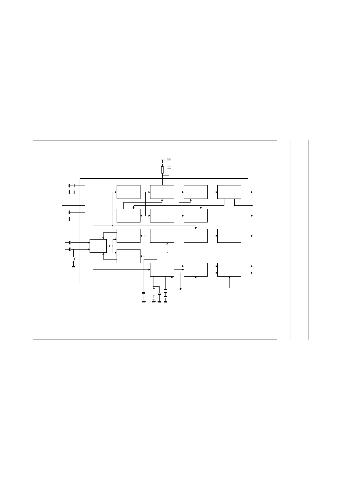
BLOCK DIAGRAM
Fig.1 Block diagram.
handbook, full pagewidth
MBE015
CHROMINANCE
BANDPASS
CHROMINANCE
TRAP
CVBS/Y
SWITCH
13
15
COINCIDENCE
DETECTOR
SYNC
SEPARATOR
PHASE
DETECTOR
VERTICAL
SYNC
SEPARATOR
OSCILLATOR
PLUS
CONTROL
H/V DIVIDER
FILTER
TUNING
NTSC
DECODER
14 22 24 18 17
MATRIX
U/V-SIGNALS
SATURATION
CONTROL
816
20
21
LUMINANCE
DELAY LINE
AMPLIFIER
19
7
2
PULSE
SHAPER
10
reference
4
PH1LF
9
DEC
DIG
11
V
P1
12
3
GND1
23
V
P2
GND2
5
DEC
BG
CVBS
CHROMA
CVBS/Y
switch
DEC
FT
PLL XTAL
HUE
SSC DEM
SW
SAT
V
U
Y
VOUT
CLAMP
HOUT
TDA8315T
Page 4
September 1994 4
Philips Semiconductors Preliminary specification
Integrated NTSC decoder
and sync processor
TDA8315T
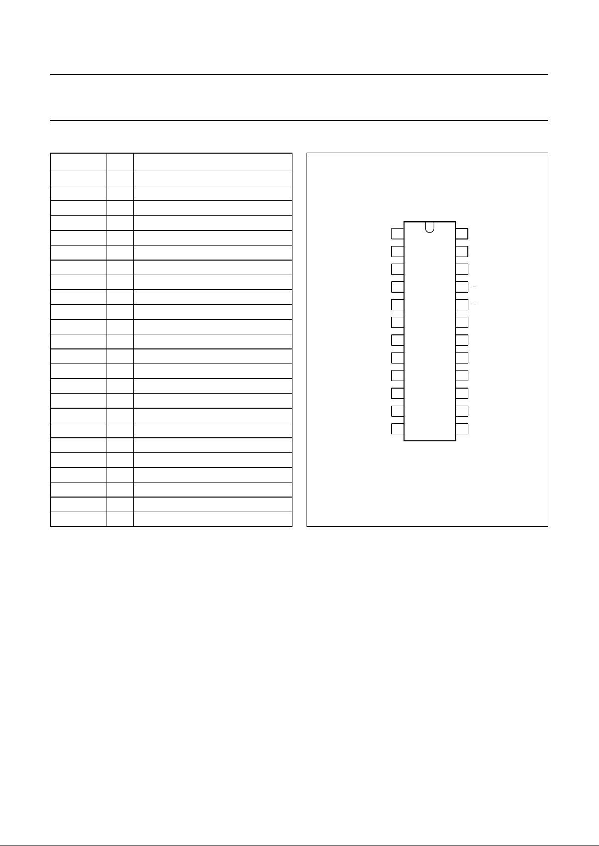
PINNING
Note
1. In the application the test pins must be connected to
ground.
SYMBOL PIN DESCRIPTION
TEST1
(1)
1 test pin 1
HOUT 2 horizontal output pulse
GND1 3 ground 1 (0 V)
PH1LF 4 phase 1 loop filter
DEC
BG
5 bandgap decoupling
TEST2
(1)
6 test pin 2
VOUT 7 vertical output pulse
DEM
SW
8 demodulation angle switch
DEC
DIG
9 decoupling digital supply
CLAMP 10 back porch clamping pulse
V
P1
11 supply voltage 1 (+8 V)
V
P2
12 supply voltage 2 (+8 V)
CVBS/Y 13 CVBS/Y input
DEC
FT
14 decoupling filter tuning
CHROMA 15 chrominance and switch input
SAT 16 saturation control input
SCS 17 sub-carrier signal output
HUE 18 hue control input
Y 19 Y output
−V20−V output
−U21−U output
PLL 22 PLL colour filter
GND2 23 ground 2 (0 V)
XTAL 24 3.58 MHz crystal connection
Fig.2 Pin configuration.
handbook, halfpage
1
2
3
4
5
6
7
8
9
10
11
12
24
23
22
21
20
19
18
17
16
15
14
13
XTAL
GND2
PLL
U
V
Y
HUE
SCS
SAT
P2
CHROMA
V
DIG
DEC
SW
DEM
DEC
BG
VOUT
TEST2
PH1LF
GND1
HOUT
TEST1
P1
CLAMP
V
CVBS/Y
DEC
FT
MBE016
TDA8315T
Page 5

September 1994 5
Philips Semiconductors Preliminary specification
Integrated NTSC decoder
and sync processor
TDA8315T
FUNCTIONAL DESCRIPTION
CVBS or Y/C input
The TDA8315T has a video input which can be switched
to CVBS (with internal chrominance bandpass and trap
filters) and to Y/C (without chrominance bandpass and
trap filters). The switching between CVBS and Y/C is
achieved by the DC level of the CHROMA input (pin 15).
Integrated video filters
The circuit contains a chrominance bandpass and trap
circuit. The filters are realised by gyrator circuits that are
automatically tuned by comparing the tuning frequency
with the crystal frequency of the decoder. The
chrominance trap can be switched off by the DC level of
the CHROMA input.
The luminance delay line is also realised by gyrator
circuits.
Colour decoder
The colour decoder contains an alignment-free crystal
oscillator, a colour killer circuit and colour difference
demodulators. The gain of the two colour difference signal
demodulators is identical and the phase angle of the
reference carrier signals is 90°. This phase shift is
achieved internally. It is possible to switch the demodulator
angle to 110° by an internal matrix circuit. The switching is
obtained externally via pin 8.
Synchronization circuit
The sync separator is preceded by a voltage controlled
amplifier which adjusts the sync pulse amplitude to a fixed
level. The sync pulses are then fed to the slicing stage
(separator) which operates at 50% of the amplitude.
The separated sync pulses are fed to the first phase
detector and to the coincidence detector. The coincidence
detector is used to detect whether the line oscillator is
synchronized. The PLL has a very high static steepness,
this ensures that the phase of the picture is independent of
the line frequency. The line oscillator operates at twice the
line frequency.
The oscillator network is internal. Because of the spread of
internal components an automatic adjustment circuit has
been added to the IC.
The circuit compares the oscillator frequency with that of
the crystal oscillator in the colour decoder. This results in
a free-running frequency which deviates less than 2% from
the typical value.
The horizontal output pulse is derived from the horizontal
oscillator via a pulse shaper. The pulse width of the output
pulse is 5.4 µs, the front edge of this pulse coincides with
the front edge of the sync pulse at the input.
The vertical output pulse is generated by a count-down
circuit. The pulse width is approximately 380 µs. Both the
horizontal and vertical pulses will always be available at
the outputs even when no input signal is available.
Page 6

September 1994 6
Philips Semiconductors Preliminary specification
Integrated NTSC decoder
and sync processor
TDA8315T
LIMITING VALUES
In accordance with the Absolute Maximum Rating System (IEC134).
THERMAL CHARACTERISTICS
CHARACTERISTICS
V
P
= 8 V; T
amb
=25°C; unless otherwise specified.
SYMBOL PARAMETER MIN. MAX. UNIT
V
P
supply voltage − 9.0 V
T
stg
storage temperature −25 +150 °C
T
amb
operating ambient temperature −25 +70 °C
T
sld
soldering temperature for 5 s − 260 °C
T
j
maximum operating junction temperature − 125 °C
SYMBOL PARAMETER VALUE UNIT
R
th j-a
thermal resistance from junction to ambient in free air ≤65 K/W
SYMBOL PARAMETER CONDITIONS MIN. TYP. MAX. UNIT
Supplies
V
P
supply voltage (pins 11 and 12) 7.2 8.0 8.8 V
I
P
supply current (pins 11 and 12) − 40 − mA
P
tot
total power dissipation − 320 − mW
CVBS or Y/C input
CVBS/Y
INPUT (PIN 13)
V
13(p-p)
CVBS/Y input voltage (peak-to-peak value) notes 1 and 2 − 1 1.4 V
I
13
CVBS/Y input current − 4 −µA
COMBINED CHROMINANCE AND SWITCH INPUT (PIN 15)
V
15(p-p)
chrominance input voltage
(peak-to-peak value)
notes 2 and 3 − 0.3 − V
V
15(p-p)
input signal amplitude before clipping
occurs (peak-to-peak value)
note 2 1 −−V
R
I
chrominance input resistance − 15 − kΩ
C
I
chrominance input capacitance note 4 −−5pF
V
15
DC input voltage for Y/C operation 345V
V
15
DC input voltage for CVBS operation −−1V
Chrominance filters and luminance delay line
C
HROMINANCE TRAP CIRCUIT
f
trap
trap frequency − 3.58 − MHz
B luminance signal bandwidth note 2 − 2.7 − MHz
SR colour subcarrier rejection 20 −−dB
Page 7

September 1994 7
Philips Semiconductors Preliminary specification
Integrated NTSC decoder
and sync processor
TDA8315T
CHROMINANCE BANDPASS CIRCUIT
f
c
centre frequency − 3.58 − MHz
QBP bandpass quality factor − 3 −
Y
DELAY LINE
t
d
delay time note 2 − 390 − ns
B bandwidth of internal delay line note 2 8 −−MHz
Y
OUTPUT SIGNAL (PIN19)
V
19(p-p)
output signal amplitude
(peak-to-peak value)
note 1 − 2.27 − V
Z
O
output impedance − 350 −Ω
V
19
top sync level − 2.85 − V
S/N signal-to-noise ratio notes 2 and 5 − 56 − dB
Colour decoder
C
HROMINANCE AMPLIFIER
ACC
cr
ACC control range note 6 24 −−dB
∆V change in amplitude of the output signals
over the ACC range
−−2dB
THR
on
threshold colour killer ON tbf −31 tbf dB
HYS
off
hysteresis colour killer OFF note 2
strong input signal S/N ≥ 40 dB − +3 − dB
noisy input signal − +1 − dB
ACL
CIRCUIT
chrominance burst ratio at which the ACL
starts to operate
2.3 − 2.7
REFERENCE PART
Phase-locked loop; note 7 (filter connected to pin 22)
f
CR
catching range 300 500 − Hz
∆ϕ phase shift for a ±400 Hz deviation of the
oscillator frequency
note 7 −−2 deg
Oscillator (pin 24)
TC
osc
temperature coefficient of f
osc
note 2 − 2.0 2.5 Hz/K
∆f
osc
f
osc
deviation with respect to V
P
note 2;
VP=8V±10%
−−250 Hz
R
I
input resistance note 4 − 1.5 − kΩ
C
I
input capacitance note 4 −−10 pF
HUE CONTROL INPUT (PIN 18)
HUE
cr
hue control range see also Fig.3 ±35 ±45 − deg
SATURATION CONTROL INPUT (PIN 16)
SAT
cr
saturation control range see also Fig.4 52 −−dB
SYMBOL PARAMETER CONDITIONS MIN. TYP. MAX. UNIT
Page 8

September 1994 8
Philips Semiconductors Preliminary specification
Integrated NTSC decoder
and sync processor
TDA8315T
DEMODULATOR OUTPUTS (PINS 20 AND 21)
B bandwidth of demodulators −3 dB; note 8 − 650 − kHz
∆VO/∆T change of output signal amplitude with
temperature
note 2 − 0.1 − %/K
∆V
O
/∆V
P
change of output signal amplitude with
supply voltage
note 2 −−±0.1 dB
G gain ratio of demodulator G(−U)/G(−V) 0.9 1.0 1.1
demodulator angle
pin 8 LOW 85 90 95 deg
pin 8 HIGH 105 110 115 deg
V
21(p-p)
−U output signal amplitude at nominal
saturation (peak-to-peak value)
note 9 − 1.5 − V
V
20(p-p)
−V output signal amplitude at nominal
saturation (peak-to-peak value)
note 9 − 1.5 − V
Z
O
output impedance (−U)/(−V) output −−500 Ω
V
O
DC output voltage − 3 − V
DEMODULATION ANGLE SWITCH INPUT (PIN 8)
V
8
input voltage for 90° angle −−1V
V
8
input voltage for 110° angle VP− 1 −−V
SUBCARRIER OUTPUT SIGNAL (PIN 17)
V
17(p-p)
output signal amplitude
(peak-to-peak value)
− 300 − mV
Z
O
output impedance − 250 −Ω
V
O
DC output voltage − 1.6 − V
Horizontal and vertical synchronization circuits
S
YNC VIDEO INPUT (PIN 13)
V
13
sync pulse amplitude note 4 50 300 − mV
SL slicing level note 10 − 50 − %
V
ERTICAL SYNC
t
W
width of the vertical sync pulse without sync
instability
note 1 1 22 −−µs
HORIZONTAL OSCILLATOR
f
fr
free-running frequency − 15734 − Hz
∆f
fr
spread on free running frequency −−±2%
∆f
osc
/∆V
P
frequency variation with respect to the
supply voltage
VP = 8 V±10%;
note 2
− 0.2 0.5 %
∆f
osc
/∆T frequency variation with temperature note 2 −−tbf Hz/K
SYMBOL PARAMETER CONDITIONS MIN. TYP. MAX. UNIT
Page 9

September 1994 9
Philips Semiconductors Preliminary specification
Integrated NTSC decoder
and sync processor
TDA8315T
HORIZONTAL PLL; NOTE 12 (FILTER CONNECTED TO PIN 4)
f
HR
holding range PLL −±0.9 ±1.2 kHz
f
CR
catching range PLL note 2 ±0.6 ±0.9 − kHz
S/N signal-to-noise ratio of the video input
signal at which the time constant is
switched
− 20 − dB
HYS hysteresis at the switching point − 3 − dB
HORIZONTAL OUTPUT (PIN 2)
V
OH
HIGH level output voltage IO= 2 mA 2.4 4.0 − V
V
OL
LOW level output voltage IO=2mA − 0.3 0.6 V
I
O(sink)
output sink current −−2mA
I
O(source)
output source current −−2mA
t
W
pulse width note 13 − 5.4 −µs
t
d
delay time between positive edge of the
horizontal output pulse and start of the
horizontal sync pulse at the input
− 0 −µs
BACK PORCH CLAMPING OUTPUT (PIN 10)
V
OH
HIGH level output voltage IO= 2 mA 2.4 4.0 − V
V
OL
LOW level output voltage IO=2mA − 0.3 0.6 V
I
O(sink)
output sink current −−2mA
I
O(source)
output source current −−2mA
t
W
pulse width 3.2 3.4 3.6 µs
t
d
delay time between start of clamping pulse
and start of the start sync pulse
5.2 5.4 5.6 µs
VERTICAL OUTPUT (PIN 7); NOTE 14
f
fr
free-running frequency − 60 − Hz
f
lock
locking range 54.6 − 64.5 Hz
divider value not locked − 525 −
locking range (lines/frame) 488 − 576
V
OH
HIGH level output voltage IO= 2 mA 2.4 4.0 − V
V
OL
LOW level output voltage IO=2mA − 0.3 0.6 V
I
O(sink)
output sink current −−2mA
I
O(source)
output source current −−2mA
t
W
pulse width (6 line periods) − 380 −µs
t
d
delay time between start of the vertical sync
pulse at the input and the positive edge of
the output pulse
− 37.5 −µs
SYMBOL PARAMETER CONDITIONS MIN. TYP. MAX. UNIT
Page 10

September 1994 10
Philips Semiconductors Preliminary specification
Integrated NTSC decoder
and sync processor
TDA8315T
Notes to the characteristics
1. Signal with negative-going sync. Amplitude includes sync pulse amplitude.
2. This parameter is not tested during production and is guaranteed by the design and qualified by matrix batches which
are made in the pilot production period.
3. Burst amplitude; for a colour bar with 75% saturation the chrominance signal amplitude is 660 mV (p-p).
4. This parameter is not tested during production and is just given as application information for the designer of the
television receiver.
5. The signal-to-noise ratio is specified as a peak-to-peak signal with respect to RMS noise (bandwidth 5 MHz).
6. At a chrominance input voltage of 660 mV (p-p) (colour bar with 75% saturation i.e. burst signal amplitude
300 mV (p-p)) the dynamic range of the ACC is +6 and −18 dB.
7. All frequency variations are referenced to 3.58 MHz carrier frequency.
All oscillator specifications are measured with the Philips crystal series 9922 520.
If the spurious response of the crystal is lower than −3 dB with respect to the fundamental frequency for a damping
resistance of 1.5 kΩ, oscillation at the fundamental frequency is guaranteed.
The catching and detuning range are measured for nominal crystal parameters. These are:
a) load resonance frequency f0 (CL = 20 pF) = 3.579545 MHz
b) motional capacitance CM = 14.5 fF
c) parallel capacitance C0 = 4.5 pF.
The actual load capacitance in the application should be CL = 18 pF to account for parasitic capacitances on
and off chip.
The free-running frequency of the oscillator can be checked by pulling the saturation control pin to the positive supply
rail. In that condition the colour killer is not active so that the frequency offset is visible on the screen.
8. This value indicates the bandwidth of the complete chrominance circuit including the chrominance bandpass filter.
The bandwidth of the demodulator low-pass filter is approximately 1 MHz.
9. Output signal amplitude for a standard colour bar signal with 75% saturation and a demodulation angle of 90°. For a
demodulation angle of 110° the −V signal amplitude will decrease to 1.2 V (p-p) and the−U signal amplitude remains
unchanged. The nominal saturation is specified as maximum −6 dB.
10. Slicing level independent of sync pulse amplitude. The slicing level of the vertical sync separator is 70% (slicing level
in direction of black level) during strong signal reception (no noise detected in the incoming signal) and 30% during
weak signal reception.
11. The horizontal and vertical sync are stable while processing Copy Guard signals and signals with phase shifted sync
pulses (stretched tapes). Trick mode conditions of the VCR will also not disturb the synchronization. The value given
is the delay caused by the vertical sync pulse integrator. The integrator has been designed such that the vertical sync
is not disturbed for special anti-copy tapes with vertical sync pulses with an on/off time of 10/22 µs.
12. To obtain a good performance for both weak signal and VCR playback the time constant of the first control loop is
switched depending on the input signal condition. Therefore the circuit contains a noise detector and the time
constant is switched to ‘slow’ when excessive noise is present in the signal. In the ‘fast’ mode during the vertical
retrace time the phase detector current is increased 50% so that phase errors due to head-switching of the VCR are
corrected as soon as possible.
To prevent the horizontal synchronization being disturbed by anti-copy guard signals such as Macrovision the phase
detector is gated during the vertical retrace period so that pulses during scan have no effect on the output voltage.
The width of the gate pulse is approximately 12 µs. during weak signal conditions (noise detector active) the gating
is active during the complete scan period and the width of the gate pulse is reduced to 5.7 µs so that the effect of the
noise is reduced to a minimum.
The output current of the phase detector in the two modes is shown in Table 1.
Page 11

September 1994 11
Philips Semiconductors Preliminary specification
Integrated NTSC decoder
and sync processor
TDA8315T
13. The horizontal output pulses are obtained from the horizontal oscillator by a pulse shaper. The width of the output
pulse is approximately 5.4 µs and the rising edge of the pulse symmetrically coincides with the start of the sync pulse
at the input.
14. The vertical output pulses are generated by a divider circuit. The vertical output pulse has a delay of 37.5 µs with
respect to the start of the vertical sync pulse at the input. This is caused by the clock frequency of the divider being
twice the horizontal frequency.
This divider circuit has 2 modes of operation:
Search mode (large window).
This mode is switched on when the circuit is not synchronized or, when a non-standard signal is received (the number
of lines per frame outside the range is between 261 and 264). In the search mode the divider can be triggered
between line 244 and line 288 (approximately 54 to 64.5 Hz).
Standard mode (narrow window).
This mode is switched on when more than 15 successive vertical sync pulses are detected in the narrow window.
When the circuit is in the standard mode and a vertical sync pulse is missing the output pulse is generated at the end
of the window. Consequently, the disturbance of the picture is very small. The circuit will switch back to the search
window when, for 6 successive vertical periods, no sync pulses are found within the window. When no input signal
is available the divider generates output pulses with a timing of 262.5 lines (standard 60 Hz signal).
Table 1 Output current of phase detector.
Note
1. Vertical retrace.
QUALITY SPECIFICATION
Quality level in accordance with SNW-FQ-611-part E.
Notes
1. All pins are protected against ESD by means of internal clamping diodes.
2. Range A is for Human body model.
3. Range B is for machine model.
Latch up
All pins meet the specification:
I
trigger
≥ 100 mA or ≥ 1.5 V
DDmax
I
trigger
≤−100 mA or ≤−0.5 V
DDmax
.
CURRENT PHASE DETECTOR DURING SCAN (µA) VERTICAL RETRACE (µA) GATED YES/NO
Weak signal and synchronized 30 30 YES (5.7 µs)
Strong signal and synchronized 180 270 YES (12 µs)
(1)
Not synchronized 180 270 NO
SYMBOL PARAMETER RANGE A
(2)
RANGE B
(3)
UNIT
ESD protection circuit specification (note 1) >2000 >200 V
100 200 pF
1500 0 Ω
Page 12

September 1994 12
Philips Semiconductors Preliminary specification
Integrated NTSC decoder
and sync processor
TDA8315T
Fig.3 Hue control curve
handbook, halfpage
MBE018
40
20
20
40
(deg)
012345
(V)
0
Fig.4 Saturation control curve.
handbook, halfpage
MBE017
200
150
100
50
0
(%)
012345
(V)
Page 13

September 1994 13
Philips Semiconductors Preliminary specification
Integrated NTSC decoder
and sync processor
TDA8315T
PACKAGE OUTLINE
Fig.5 Plastic small outline package; 24 leads; large body (SO24, SOT137-1).
Dimensions in mm.
handbook, full pagewidth
7.6
7.4
10.65
10.00
A
MBC235 - 1
0.3
0.1
2.45
2.25
1.1
0.5
0.32
0.23
1.1
1.0
0 to 8
o
2.65
2.35
detail A
S
15.6
15.2
0.1 S
112
1324
pin 1
index
0.9
0.4
(4x)
0.25 M
(24x)
0.49
0.36
1.27
Page 14

September 1994 14
Philips Semiconductors Preliminary specification
Integrated NTSC decoder
and sync processor
TDA8315T
SOLDERING
Plastic small-outline packages
B
YWAVE
During placement and before soldering, the component
must be fixed with a droplet of adhesive. After curing the
adhesive, the component can be soldered. The adhesive
can be applied by screen printing, pin transfer or syringe
dispensing.
Maximum permissible solder temperature is 260 °C, and
maximum duration of package immersion in solder bath is
10 s, if allowed to cool to less than 150 °C within 6 s.
Typical dwell time is 4 s at 250 °C.
A modified wave soldering technique is recommended
using two solder waves (dual-wave), in which a turbulent
wave with high upward pressure is followed by a smooth
laminar wave. Using a mildly-activated flux eliminates the
need for removal of corrosive residues in most
applications.
B
Y SOLDER PASTE REFLOW
Reflow soldering requires the solder paste (a suspension
of fine solder particles, flux and binding agent) to be
applied to the substrate by screen printing, stencilling or
pressure-syringe dispensing before device placement.
Several techniques exist for reflowing; for example,
thermal conduction by heated belt, infrared, and
vapour-phase reflow. Dwell times vary between 50 and
300 s according to method. Typical reflow temperatures
range from 215 to 250 °C.
Preheating is necessary to dry the paste and evaporate
the binding agent. Preheating duration: 45 min at 45 °C.
R
EPAIRING SOLDERED JOINTS (BY HAND-HELD SOLDERING
IRON OR PULSE
-HEATED SOLDER TOOL)
Fix the component by first soldering two, diagonally
opposite, end pins. Apply the heating tool to the flat part of
the pin only. Contact time must be limited to 10 s at up to
300 °C. When using proper tools, all other pins can be
soldered in one operation within 2 to 5 s at between 270
and 320 °C. (Pulse-heated soldering is not recommended
for SO packages.)
For pulse-heated solder tool (resistance) soldering of VSO
packages, solder is applied to the substrate by dipping or
by an extra thick tin/lead plating before package
placement.
Page 15

September 1994 15
Philips Semiconductors Preliminary specification
Integrated NTSC decoder
and sync processor
TDA8315T
DEFINITIONS
LIFE SUPPORT APPLICATIONS
These products are not designed for use in life support appliances, devices, or systems where malfunction of these
products can reasonably be expected to result in personal injury. Philips customers using or selling these products for
use in such applications do so at their own risk and agree to fully indemnify Philips for any damages resulting from such
improper use or sale.
Data sheet status
Objective specification This data sheet contains target or goal specifications for product development.
Preliminary specification This data sheet contains preliminary data; supplementary data may be published later.
Product specification This data sheet contains final product specifications.
Limiting values
Limiting values given are in accordance with the Absolute Maximum Rating System (IEC 134). Stress above one or
more of the limiting values may cause permanent damage to the device. These are stress ratings only and operation
of the device at these or at any other conditions above those given in the Characteristics sections of the specification
is not implied. Exposure to limiting values for extended periods may affect device reliability.
Application information
Where application information is given, it is advisory and does not form part of the specification.
Page 16

Philips Semiconductors
Philips Semiconductors – a worldwide company
Argentina: IEROD, Av. Juramento 1992 - 14.b, (1428)
BUENOS AIRES, Tel. (541)786 7633, Fax. (541)786 9367
Australia: 34 Waterloo Road, NORTH RYDE, NSW 2113,
Tel. (02)805 4455, Fax. (02)805 4466
Austria: Triester Str. 64, A-1101 WIEN, P.O. Box 213,
Tel. (01)60 101-1236, Fax. (01)60 101-1211
Belgium: Postbus 90050, 5600 PB EINDHOVEN, The Netherlands,
Tel. (31)40 783 749, Fax. (31)40 788 399
Brazil: Rua do Rocio 220 - 5
th
floor, Suite 51,
CEP: 04552-903-SÃO PAULO-SP, Brazil.
P.O. Box 7383 (01064-970).
Tel. (011)821-2333, Fax. (011)829-1849
Canada: PHILIPS SEMICONDUCTORS/COMPONENTS:
Tel. (800) 234-7381, Fax. (708) 296-8556
Chile: Av. Santa Maria 0760, SANTIAGO,
Tel. (02)773 816, Fax. (02)777 6730
Colombia: IPRELENSO LTDA, Carrera 21 No. 56-17,
77621 BOGOTA, Tel. (571)249 7624/(571)217 4609,
Fax. (571)217 4549
Denmark: Prags Boulevard 80, PB 1919, DK-2300 COPENHAGEN S,
Tel. (032)88 2636, Fax. (031)57 1949
Finland: Sinikalliontie 3, FIN-02630 ESPOO,
Tel. (9)0-50261, Fax. (9)0-520971
France: 4 Rue du Port-aux-Vins, BP317,
92156 SURESNES Cedex,
Tel. (01)4099 6161, Fax. (01)4099 6427
Germany: P.O. Box 10 63 23, 20043 HAMBURG,
Tel. (040)3296-0, Fax. (040)3296 213.
Greece: No. 15, 25th March Street, GR 17778 TAVROS,
Tel. (01)4894 339/4894 911, Fax. (01)4814 240
Hong Kong: PHILIPS HONG KONG Ltd., 6/F Philips Ind. Bldg.,
24-28 Kung Yip St., KWAI CHUNG, N.T.,
Tel. (852)424 5121, Fax. (852)428 6729
India: Philips INDIA Ltd, Shivsagar Estate, A Block ,
Dr. Annie Besant Rd. Worli, Bombay 400 018
Tel. (022)4938 541, Fax. (022)4938 722
Indonesia: Philips House, Jalan H.R. Rasuna Said Kav. 3-4,
P.O. Box 4252, JAKARTA 12950,
Tel. (021)5201 122, Fax. (021)5205 189
Ireland: Newstead, Clonskeagh, DUBLIN 14,
Tel. (01)640 000, Fax. (01)640 200
Italy: PHILIPS SEMICONDUCTORS S.r.l.,
Piazza IV Novembre 3, 20124 MILANO,
Tel. (0039)2 6752 2531, Fax. (0039)2 6752 2557
Japan: Philips Bldg 13-37, Kohnan 2-chome, Minato-ku, TOKYO 108,
Tel. (03)3740 5028, Fax. (03)3740 0580
Korea: (Republic of) Philips House, 260-199 Itaewon-dong,
Yongsan-ku, SEOUL, Tel. (02)794-5011, Fax. (02)798-8022
Malaysia: No. 76 Jalan Universiti, 46200 PETALING JAYA,
SELANGOR, Tel. (03)750 5214, Fax. (03)757 4880
Mexico: 5900 Gateway East, Suite 200, EL PASO, TX 79905,
Tel. 9-5(800)234-7381, Fax. (708)296-8556
Netherlands: Postbus 90050, 5600 PB EINDHOVEN, Bldg. VB
Tel. (040)783749, Fax. (040)788399
New Zealand: 2 Wagener Place, C.P.O. Box 1041, AUCKLAND,
Tel. (09)849-4160, Fax. (09)849-7811
Norway: Box 1, Manglerud 0612, OSLO,
Tel. (022)74 8000, Fax. (022)74 8341
Pakistan: Philips Electrical Industries of Pakistan Ltd.,
Exchange Bldg. ST-2/A, Block 9, KDA Scheme 5, Clifton,
KARACHI 75600, Tel. (021)587 4641-49,
Fax. (021)577035/5874546.
Philippines: PHILIPS SEMICONDUCTORS PHILIPPINES Inc,
106 Valero St. Salcedo Village, P.O. Box 2108 MCC, MAKATI,
Metro MANILA, Tel. (02)810 0161, Fax. (02)817 3474
Portugal: PHILIPS PORTUGUESA, S.A.,
Rua dr. António Loureiro Borges 5, Arquiparque - Miraflores,
Apartado 300, 2795 LINDA-A-VELHA,
Tel. (01)14163160/4163333, Fax. (01)14163174/4163366.
Singapore: Lorong 1, Toa Payoh, SINGAPORE 1231,
Tel. (65)350 2000, Fax. (65)251 6500
South Africa: S.A. PHILIPS Pty Ltd.,
195-215 Main Road Martindale, 2092 JOHANNESBURG,
P.O. Box 7430 Johannesburg 2000,
Tel. (011)470-5911, Fax. (011)470-5494.
Spain: Balmes 22, 08007 BARCELONA,
Tel. (03)301 6312, Fax. (03)301 42 43
Sweden: Kottbygatan 7, Akalla. S-164 85 STOCKHOLM,
Tel. (0)8-632 2000, Fax. (0)8-632 2745
Switzerland: Allmendstrasse 140, CH-8027 ZÜRICH,
Tel. (01)488 2211, Fax. (01)481 77 30
Taiwan: PHILIPS TAIWAN Ltd., 23-30F, 66, Chung Hsiao West
Road, Sec. 1. Taipeh, Taiwan ROC, P.O. Box 22978,
TAIPEI 100, Tel. (02)388 7666, Fax. (02)382 4382.
Thailand: PHILIPS ELECTRONICS (THAILAND) Ltd.,
209/2 Sanpavuth-Bangna Road Prakanong,
Bangkok 10260, THAILAND,
Tel. (662)398-0141, Fax. (662)398-3319.
Turkey:Talatpasa Cad. No. 5, 80640 GÜLTEPE/ISTANBUL,
Tel. (0212)279 2770, Fax. (0212)269 3094
United Kingdom: Philips Semiconductors LTD.,
276 Bath road, Hayes, MIDDLESEX UB3 5BX,
Tel. (081)73050000, Fax. (081)7548421
United States:811 East Arques Avenue, SUNNYVALE,
CA 94088-3409, Tel. (800)234-7381, Fax. (708)296-8556
Uruguay: Coronel Mora 433, MONTEVIDEO,
Tel. (02)70-4044, Fax. (02)92 0601
For all other countries apply to: Philips Semiconductors,
International Marketing and Sales, Building BE-p,
P.O. Box 218, 5600 MD, EINDHOVEN, The Netherlands,
Telex 35000 phtcnl, Fax. +31-40-724825
SCD34 © Philips Electronics N.V. 1994
All rights are reserved. Reproduction in whole or in part is prohibited without the
prior written consent of the copyright owner.
The information presented in this document does not form part of any quotation
or contract, is believed to be accurate and reliable and may be changed without
notice. No liability will be accepted by the publisher for any consequence of its
use. Publication thereof does not convey nor imply any license under patent- or
other industrial or intellectual property rights.
Printed in The Netherlands
533061/1500/01/pp16 Date of release: September 1994
Document order number: 9397 739 00011
 Loading...