

Page 1

INTEGRATED CIRCUITS
DATA SH EET
TDA8310
PAL/NTSC colour processor for
PIP applications
Preliminary specification
File under Integrated Circuits, IC02
Philips Semiconductors
February 1995
Page 2

Philips Semiconductors Preliminary specification
PAL/NTSC colour processor for
PIP applications
FEATURES
• Multistandard vision IF circuit (positive and negative
modulation)
• Video switch which automatically detects whether the
incoming signal is CVBS or Y/C
• Integrated chrominance trap and bandpass filters
(automatically calibrated)
• Integrated luminance delay line
• Automatic PAL/NTSC decoder which can decode all
standards available in the world
• Easy interfacing with the TDA8395 (SECAM decoder)
for multistandard applications
• Horizontal PLL with an alignment-free horizontal
oscillator
• Vertical count-down circuit
• RGB/YUV and fast blanking switch with 3-state output
and active clamping
• Low dissipation (560 mW)
• Small amount of peripheral components compared with
competition ICs.
TDA8310
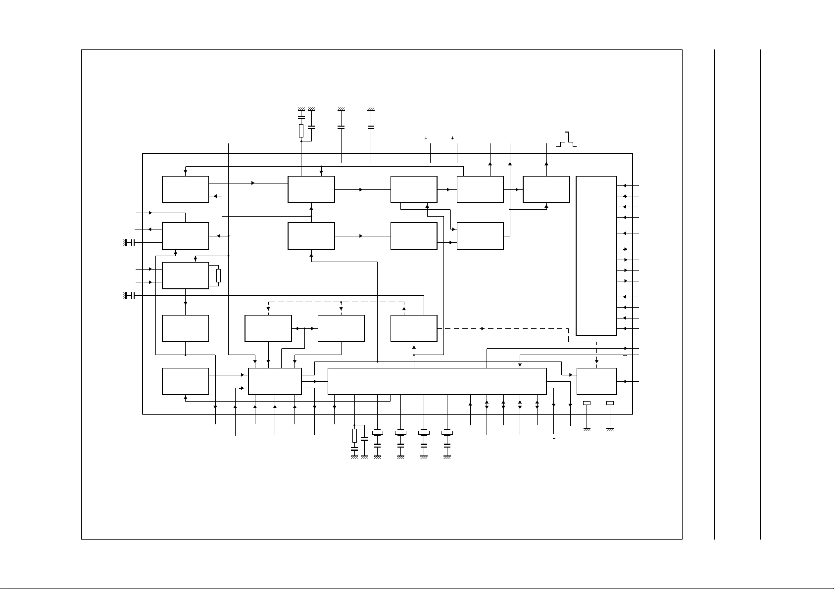
GENERAL DESCRIPTION
The TDA8310 is an alignment-free PAL/NTSC colour
processor for Picture-in-Picture (PIP) applications. The
circuit contains a vision IF amplifier, a PAL/NTSC colour
decoder, horizontal and vertical synchronization and an
RGB/YUV switch.
As input for the colour decoder and sync processor the
demodulated IF signal can be chosen but the circuit also
has a video input which automatically detects whether the
incoming signal is CVBS or Y/C. The output signals for the
PIP processor are:
Luminance signal
Colour difference signals (U and V)
Horizontal and vertical synchronization pulses.
The RGB/YUV switch can select between two RGB or
YUV sources, e.g. between the PIP processor and the
SCART input signal.
The supply voltage for the IC is 8 V. It is available in a
52-pin SDIP package.
ORDERING INFORMATION
TYPE NUMBER
NAME DESCRIPTION VERSION
TDA8310 SDIP52 plastic shrink dual in-line package; 52 leads (600 mil) SOT247-1
PACKAGE
February 1995 2
Page 3
Philips Semiconductors Preliminary specification
PAL/NTSC colour processor for
PIP applications
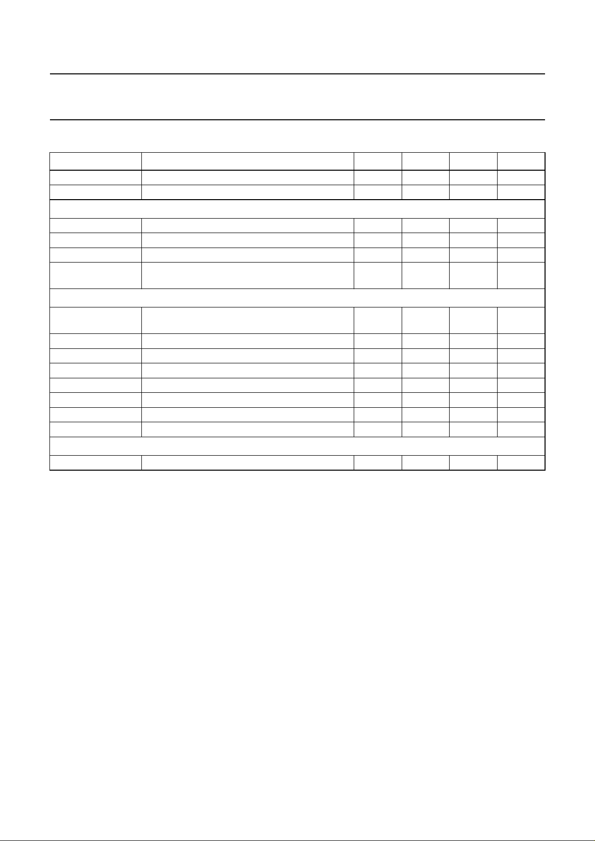
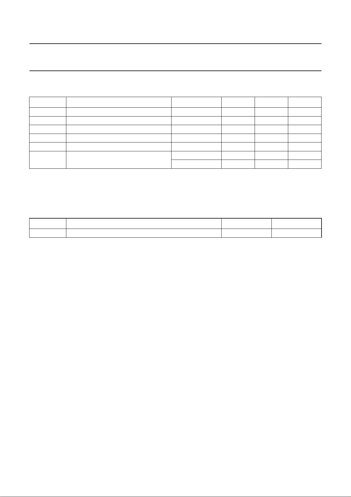
QUICK REFERENCE DATA
SYMBOL PARAMETER MIN. TYP. MAX. UNIT
V
P
I
P
Input voltages
V
i(rms)
V
17,20(p-p)
V
16(p-p)
V
i(p-p)
Output signals
V
o(p-p)
V
29
V
o(p-p)
V
50(p-p)
V
51(p-p)
V
39
V
36
G
v
Control voltage
V
control
supply voltage (pins 19 and 41) 7.2 8.0 8.8 V
supply current − 70 − mA
vision IF amplifier input sensitivity (RMS value) − 70 100 µV
CVBS/Y input voltage (peak-to-peak value) − 1 1.4 V
chrominance input voltage (peak-to-peak value) − 0.3 − V
RGB/YUV input signal voltage amplitude
−−1.3 V
(peak-to-peak value)
demodulated CVBS output voltage
− 2.5 − V
(peak-to-peak value)
tuner AGC control output voltage 0 − 12 V
luminance output voltage (peak-to-peak value) − 1.4 − V
(B−Y) output voltage (peak-to-peak value) 1.06 1.33 1.60 V
(R−Y) output voltage (peak-to-peak value) 0.84 1.05 1.26 V
horizontal sync pulse output voltage − 4 − V
vertical sync pulse output voltage − 4 − V
voltage gain of the RGB switches −0.5 0 +0.5 dB
control voltage for HUE 0 − 5V
TDA8310
February 1995 3
Page 4
February 1995 4
BLOCK DIAGRAM
PIP applications
V
V
P2
CVBS
sw
PH1LF
37
DEC
35
BG
DEC
21
DIG
( 8 V)
P1
19
HOUT36VOUT
39
( 8 V)
41
SAND
40
Philips Semiconductors Preliminary specification
PAL/NTSC colour processor for
TUNER
TUNER
C
AGC
DEC
COINCIDENCE/
NOISE
DETECTOR
31
ADJ
29
30
33
34
15
AGC FOR
IF AND
TUNER
VIF
AMPLIFIER
DEMODULATOR
VIDEO
AMPLIFIER
AUTOMATIC
Y/C
DETECTOR
VIDEO
22
CVBS
CHROMINANCE
BANDPASS
SELECTOR
20
CVBS
EXT
INT
INPUT
SYST
AGC
IF1
IF2
FT
917
CHROMA
sw
PHASE
DETECTOR
SYNC
SEPARATOR
CHROMINANCE
16
47
1
CHROMA
TRAP
SECAM
0
48
46 45
PLL XTAL4
VCO
+
CONTROL
VERTICAL
SYNC
SEPARATOR
FILTER
TUNING
REF
PAL/NTSC
DECODER
41
XTAL343XTAL242XTAL1
PULSE
SHAPER
HORIZONTAL/
VERTICAL
DIVIDER
27 26
R/W
COLOUR2
COLOUR1
TDA8310
25
LOGIC1
SANDCASTLE
GENERATOR
23
24
LOGIC2
B Y
50 51
R Y
RGB/YUV
SWITCH
LUMINANCE
DELAY LINE
18 38
GND1 GND2
10
R1
11
G1
12
B1
13
BLANK1
14
CLAMP
8
R
7
G
6
B
5
BLANK
1
R2
2
G2
3
B2
52
BLANK2
4
IDENT
HUE
28
49
Y
MBE245
Fig.1 Block diagram.
handbook, full pagewidth
TDA8310
Page 5
Philips Semiconductors Preliminary specification
PAL/NTSC colour processor for
PIP applications
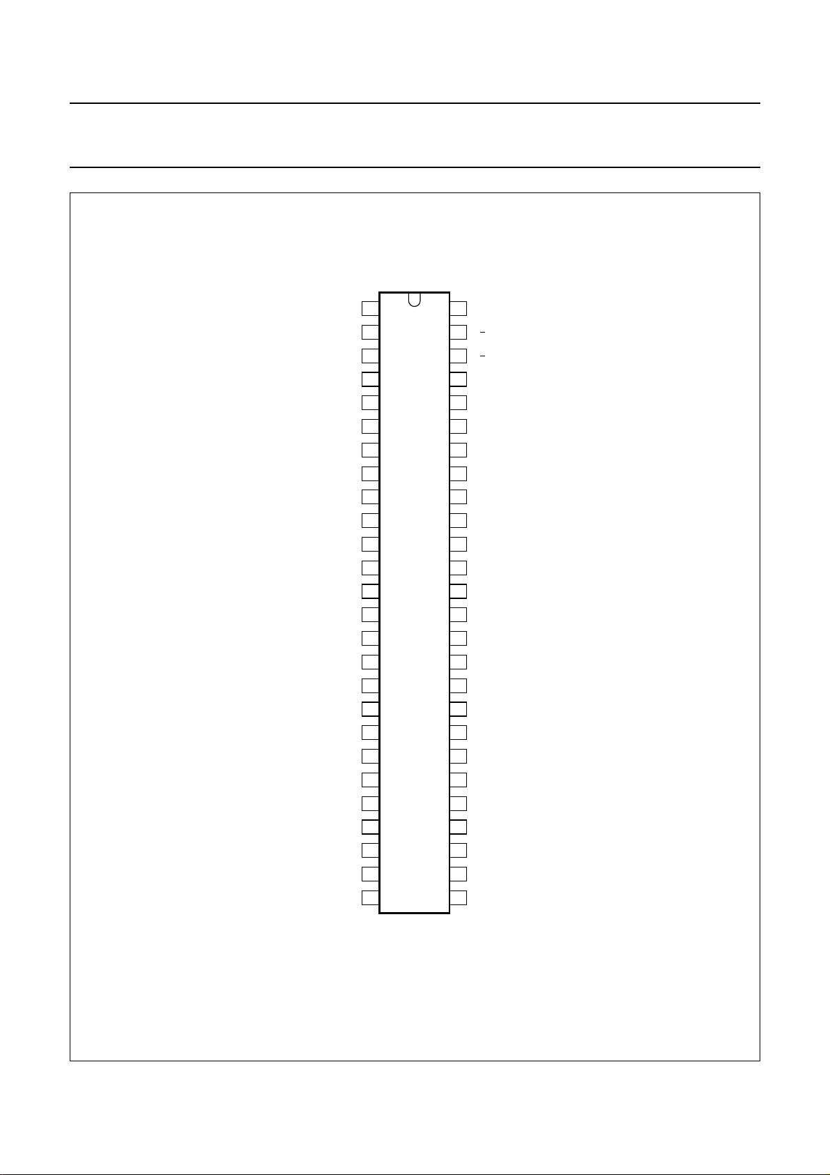
PINNING
SYMBOL PIN DESCRIPTION
R2 1 RED input 2 (PIP)
G2 2 GREEN input 2 (PIP)
B2 3 BLUE input 2 (PIP)
IDENT 4 colour standard identification output
BLANK 5 blanking output
B 6 BLUE output
G 7 GREEN output
R 8 RED output
SYST
SW
R1 10 RED input 1
G1 11 GREEN input 1
B1 12 BLUE input 1
BLANK1 13 blanking input 1
CLAMP 14 clamping pulse input
DEC
FT
CHROMA
CVBS
EXT
GND1 18 ground 1 (0 V)
V
P1
CVBS
INT
DEC
DIG
VIDEO 22 IF video output
LOGIC2 23 crystal logic 2 input/output
LOGIC1 24 crystal logic 1 input/output
COLOUR2 25 colour system logic 2 input/output
COLOUR1 26 colour system logic 1 input/output
R/W 27 read/write selection input
9 system switch
15 decoupling filter tuning
16 chrominance input
I
17 external CVBS input
19 supply voltage 1 (+8 V)
20 internal CVBS input
21 decoupling digital supply
TDA8310
SYMBOL PIN DESCRIPTION
HUE 28 HUE control input
TUNER
C
AGC
TUNER
CVBS
SW
IF1 33 IF input 1
IF2 34 IF input 2
DEC
BG
VOUT 36 vertical sync output pulse
PH1LF 37 phase 1 loop filter
GND2 38 ground 2 (0 V)
HOUT 39 horizontal sync output pulse
SAND 40 sandcastle pulse output
V
P2
XTAL1 42 4.4336 MHz crystal
XTAL2 43 3.5820 MHz crystal for PAL-N
XTAL3 44 3.5756 MHz crystal for PAL-M
XTAL4 45 3.5795 MHz crystal for NTSC
PLL 46 PLL colour filter
CHROMA
SECAM 48 SECAM reference output
Y 49 Y output
B−Y50B−Y output
R−Y51R−Y output
BLANK2 52 blanking/insertion input 2 (PIP)
29 tuner AGC output
AGC
30 AGC filter capacitor
31 tuner take-over adjustment input
ADJ
32 CVBS positive/negative modulation
control switch input
35 bandgap decoupling
41 supply voltage 2 (+8 V)
47 chrominance output for TDA8395
O
February 1995 5
Page 6
Philips Semiconductors Preliminary specification
PAL/NTSC colour processor for
PIP applications
handbook, halfpage
R2
G2
B2
IDENT
BLANK
SYST
SW
R1
G1
B1
BLANK1
CLAMP
DEC
FT
CHROMA
CVBS
EXT
GND1
V
P1
CVBS
INT
DEC
DIG
VIDEO
LOGIC2
LOGIC1
COLOUR2
COLOUR1
B
G
R
I
1
2
3
4
5
6
7
8
9
10
11
12
13
14
15
16
17
18
19
20
21
22
23
24
25
26
TDA8310
MBE244
52
51
50
49
48
47
46
45
44
43
42
41
40
39
38
37
36
35
34
33
32
31
30
29
28
27
BLANK2
R Y
B Y
Y
SECAM
CHROMA
PLL
XTAL4
XTAL3
XTAL2
XTAL1
V
P2
SAND
HOUT
GND2
PH1LF
VOUT
DEC
BG
IF2
IF1
CVBS
SW
TUNER
C
AGC
TUNER
HUE
R/W
TDA8310
O
ADJ
AGC
Fig.2 Pin configuration.
February 1995 6
Page 7

Philips Semiconductors Preliminary specification
PAL/NTSC colour processor for
PIP applications
FUNCTIONAL DESCRIPTION
Vision IF amplifier
The IF amplifier contains three AC-coupled control stages
with a total gain control range >60 dB. The sensitivity of
the circuit is comparable with that of modern IF-ICs. The
demodulation of the IF signal is achieved by a multiplier.
The demodulator is alignment-free and does not require
external components.
The polarity of the demodulator can be switched to make
the circuit suitable for positive and negative modulated
signals.
The AGC detector operates on top-sync or top white-level
depending on the position of the demodulator. The AGC
detector time-constant capacitor is externally connected to
facilitate flexibility of the application. During positive
modulation the time-constant of the AGC system is too
long to avoid visible variations of the signal amplitude. To
obtain an acceptable speed of the AGC system a circuit
has been included which detects whether the AGC
detector is activated every frame period. When no action
is detected during three frame periods the speed of the
system is increased.
Synchronization circuit
The sync separator is preceded by a voltage controlled
amplifier which adjusts the sync pulse amplitude to a fixed
level. The sync pulses are then fed to the slicing stage
(separator) which operates at 50% of the amplitude.
The separated sync pulses are fed to the first phase
detector and to the coincidence detector. The coincidence
detector is used to detect whether the line oscillator is
synchronized and for transmitter identification. The first
PLL has a very high static steepness, this ensures that the
phase of the picture is independent of the line frequency.
The line oscillator operates at twice the line frequency.
The oscillator network is internal. Because of the spread of
internal components an automatic adjustment circuit has
been added to the IC.
The circuit compares the oscillator frequency with that of
the crystal oscillator in the colour decoder. This results in
a free-running frequency which deviates less than 2% from
the typical value.
The horizontal output pulse is derived from the horizontal
oscillator via a pulse shaper. The pulse width of the output
pulse is 5.4 µs, the front edge of this pulse coincides with
the front edge of the sync pulse at the input.
TDA8310
The vertical output pulse is generated by a count-down
circuit. The pulse width is approximately 380 µs. Both the
horizontal and vertical pulses will always be available at
the outputs even when no input signal is available.
In addition to the horizontal and vertical sync pulse outputs
the IC has a sandcastle pulse output which contains burst
key and blanking pulses.
Integrated video filters
The circuit contains a chrominance bandpass and trap
circuit. The filters are realised by gyrator circuits that are
automatically tuned by comparing the tuning frequency
with the crystal frequency of the decoder. When a Y/C
signal is supplied to the input the chrominance trap is
automatically switched off by the Y/C detection circuit, but
it is also possible to force the filters in the CVBS or Y/C
position.
The luminance delay line is also realised by gyrator
circuits.
Colour decoder
The colour decoder contains an alignment-free crystal
oscillator, a colour killer circuit and colour difference
demodulators. The 90° phase shift for the reference signal
is achieved internally.
The colour decoder is very flexible. Together with the
SECAM decoder TDA8395 an automatic multistandard
decoder can be designed but it is also possible to use it for
one standard when only one crystal is connected to the IC.
The decoder can be forced to one of the standards via the
“forced mode” pins. The crystal pins which are not used
must be connected to the positive supply line via a 8.2 kΩ
resistor. It is also possible to connect the non-used pins
with one resistor to the positive supply line. In this event
the resistor must have a value of 8.2 kΩ divided by the
number of pins.
The chrominance output signal of the video switch is
externally available and must be used as an input signal
for the SECAM decoder.
RGB/YUV switch
The RGB/YUV switch is for switching between two RGB or
YUV video sources. The outputs of the switch can be set
to high impedance state so that other switches can be
used in parallel.
The switch is controlled via pins 13 and 52. The details of
switch control are shown in Table 5.
February 1995 7
Page 8
Philips Semiconductors Preliminary specification
PAL/NTSC colour processor for
TDA8310
PIP applications
LIMITING VALUES
In accordance with the Absolute Maximum Rating System (IEC134).
SYMBOL PARAMETER CONDITIONS MIN. MAX. UNIT
V
P
T
stg
T
amb
T
sld
T
j
V
es
Notes
1. Human body model 100 pF, 1500 Ω.
2. Machine model 200 pF, 0 Ω.
THERMAL CHARACTERISTICS
SYMBOL PARAMETER VALUE UNIT
R
th j-a
supply voltage − 9.0 V
storage temperature −25 +150 °C
operating ambient temperature −25 +70 °C
soldering temperature for 5 s − 260 °C
maximum operating junction temperature − 150 °C
electrostatic discharge note 1 −2000 +2000 V
note 2 −200 +200 V
thermal resistance from junction to ambient in free air ≤40 K/W
QUALITY SPECIFICATION
In accordance with
“SNW-FQ-611 part E”
Reference Handbook”
. The handbook can be ordered using the code 9398 510 63011. All pins are protected against
. The numbers of the quality specification can be found in the
electrostatic discharge by means of internal clamping diodes.
Latch up
At T
=70°C most pins meet the specification:
amb
I
≥ 100 mA or ≥ 1.5 V
trigger
I
≤−100 mA or ≤−0.5 V
trigger
DDmax
DDmax
.
The following pins do not meet this specification:
pin 7 +90 mA
pin 21 +90 mA
pin 32 −90 mA
pin 46 +90 mA.
“Quality
February 1995 8
Page 9

Philips Semiconductors Preliminary specification
PAL/NTSC colour processor for
TDA8310
PIP applications
CHARACTERISTICS
V
=8V; T
P
SYMBOL PARAMETER CONDITIONS MIN. TYP. MAX. UNIT
Supplies
V
P
I
P1
I
P2
P
tot
IF circuit
V
ISION IF AMPLIFIER INPUT (PINS 33 AND 34)
V
i(rms)
R
I
C
I
G
cr
V
i(rms)
VIDEO AMPLIFIER OUTPUT;note4(PIN 22)
V
22(neg)
V
22(pos)
∆V
22
Z
O
I
bias
I
source
S/N signal-to-noise ratio notes 6 and 7
V
22(rc)
=25°C; unless otherwise specified.
amb
supply voltage (pins 19 and 41) 7.2 8.0 8.8 V
supply current (pin 19) 45 65 80 mA
supply current (pin 41) 3 5 10 mA
total power dissipation − 560 − mW
input sensitivity (RMS value) note 1
= 38.90 MHz − 70 100 µV
f
i
f
= 45.75 MHz − 70 100 µV
i
f
= 58.75 − 70 100 µV
i
Input resistance (differential) note 2 1.6 2.0 2.4 kΩ
Input capacitance (differential) note 2 − 3 − pF
gain control range note 3 64 −−dB
maximum input signal (RMS value) 100 150 − mV
negative modulation
zero signal output level note 5 4.45 4.60 4.75 V
top sync level 1.9 2.0 2.1 V
positive modulation
zero signal output level note 5 1.85 2.00 2.15 V
white level 4.2 4.3 4.4 V
difference in amplitude between
− 015%
negative and positive modulation
video output impedance −−75 Ω
internal bias current of NPN emitter
1 −−mA
follower output transistor
maximum source current −−5mA
V
=10mV 52 60 − dB
i
end of control range 52 61 − dB
residual carrier signal note 6 − 2.5 − mV
February 1995 9
Page 10

Philips Semiconductors Preliminary specification
PAL/NTSC colour processor for
TDA8310
PIP applications
SYMBOL PARAMETER CONDITIONS MIN. TYP. MAX. UNIT
IF AND TUNER AGC
Timing of IF-AGC (C30= 2.2µF)
modulated video interference 30% AM for 1 to 100 mV;
t
inc
response time for an IF input signal
amplitude increase of 52 dB for
positive and negative modulation
t
dec
response time for an IF input signal
amplitude decrease of 52 dB
for negative modulation − 25 50 ms
for positive modulation − 100 200 ms
I
leak
allowed leakage current of the AGC
capacitor
for negative modulation −−10 µA
for positive modulation −−200 nA
Tuner take-over adjustment (pin 31)
V
31(rms)
minimum starting level voltage for
tuner take-over (RMS value)
V
31(rms)
maximum starting level voltage for
tuner take-over (RMS value)
V
cr
control voltage range 0.5 − 4.5 V
Tuner control output (pin 29)
V
29
V
29(sat)
I
29
maximum tuner AGC output voltage maximum gain −−12 V
output saturation voltage minimum gain;
maximum tuner AGC output current
swing
I
leak
∆V
29
leakage current RF AGC −−1µA
input signal voltage variation for
complete tuner control
0 to 200 Hz (system B/G)
note 8
I29=2mA
I
= 1 mA 0.5 2.0 4.0 dB
O(max)
−−10 %
− 25ms
− 0.2 0.5 mV
100 150 − mV
−−300 mV
5 −−mA
CVBS and Y/C switch
I
NTERNAL CVBS AND EXTERNAL CVBS/Y INPUTS (PINS 20 AND 17)
V
20,17(p-p)
CVBS/Y input voltage
notes 2 and 9 − 1 1.4 V
(peak-to-peak value)
I
20,17
V
clamp
I
clamp
input current − 46µA
top sync clamping voltage level − 3.3 − V
clamping input current 80 100 −µA
February 1995 10
Page 11

Philips Semiconductors Preliminary specification
PAL/NTSC colour processor for
TDA8310
PIP applications
SYMBOL PARAMETER CONDITIONS MIN. TYP. MAX. UNIT
CHROMINANCE INPUT (PIN 16)
V
16(p-p)
chrominance input voltage
(peak-to-peak value)
V
16(p-p)
input signal amplitude before clipping
occurs (peak-to-peak value)
R
I
C
I
chrominance input resistance 14 20 26 kΩ
chrominance input capacitance note 2 −−5pF
CHROMINANCE OUTPUT (PIN 47)
V
47(p-p)
output signal voltage amplitude
(peak-to-peak value)
Z
O
V
O
output impedance 200 250 300 Ω
DC output voltage open-circuit output 1.2 1.4 1.6 V
SWITCH CONTROL INPUT FOR INTERNAL/EXTERNAL POSITIVE/NEGATIVE MODULATION; note 11 (PIN 32)
V
32
internal CVBS signal selected
with negative modulation −−1V
with positive modulation note 12 2 − 3V
V
32
Z
I
external CVBS or Y/C signal selected IF switched to negative
input impedance 25 −−kΩ
ISS suppression of non-selected video
input signal
S
WITCH CONTROL INPUT FOR EXTERNAL CVBS OR Y/C SELECTION (PIN 9)
V
9
V
9
V
9
Z
I
filters switched to CVBS condition −−1V
filters switched to Y/C condition note 12 2 − 3V
automatic selection of CVBS or Y/C 3.9 − V
input impedance 25 −−kΩ
Chrominance filters, luminance delay line and luminance output
notes 2, 10 and 17 − 0.3 − V
note 6 1.0 −−V
0.18 0.20 0.22 V
3.9 − V
P
V
modulation
note 6 50 −−dB
P
V
C
HROMINANCE TRAP CIRCUIT
f
trap
trap frequency − f
osc
− MHz
QF trap quality factor notes 6 and 13 − 2 −
SR colour subcarrier rejection 20 −−dB
CHROMINANCE BANDPASS CIRCUIT
f
c
centre frequency − f
osc
− MHz
QBP bandpass quality factor note 6 − 3 −
Y
DELAY LINE
∆t
d
difference in delay time between the
note 6 0 50 100 ns
luminance and the demodulated
chrominance signals
B bandwidth of internal delay line note 6 8 −−MHz
February 1995 11
Page 12

Philips Semiconductors Preliminary specification
PAL/NTSC colour processor for
TDA8310
PIP applications
SYMBOL PARAMETER CONDITIONS MIN. TYP. MAX. UNIT
Y OUTPUT (PIN 49)
V
49(b-w)
output signal voltage amplitude
(black-to-white value)
Z
O
V
49(DC)
I
bias
output impedance 80 100 120 Ω
DC output voltage level (top sync) 2.7 2.9 3.1 V
internal bias current of NPN emitter
follower output transistor
I
source
maximum source current −−2mA
Horizontal and vertical synchronization circuits
S
YNC VIDEO INPUT (PINS 17 AND 20)
V
17,20
sync pulse voltage amplitude note 2 50 300 − mV
SL slicing level note 14 − 50 − %
VERTICAL SYNC
t
W
width of the vertical sync pulse
without sync instability
HORIZONTAL OSCILLATOR
f
fr
∆f
fr
∆f
/∆V
osc
free running frequency − 15625 − Hz
spread on free running frequency −−±2%
frequency variation with respect to
P
the supply voltage
∆f
osc
∆f
osc( max
frequency variation with temperature T
) maximum frequency deviation at the
start of the horizontal output
HORIZONTAL PLL; note 16 (FILTER CONNECTED TO PIN 37)
f
HR
f
CR
holding range PLL −±0.9 ±1.2 kHz
catching range PLL note 6 ±0.6 ±0.9 − kHz
S/N signal-to-noise ratio of the video
input signal at which the time
constant is switched
HYS hysteresis at the switching point 1 3 6 dB
HORIZONTAL OUTPUT (PIN 39)
V
OH
V
OL
I
sink
I
source
t
W
t
d
HIGH level output voltage IO= 2 mA 2.4 4.0 − V
LOW level output voltage IO=2mA − 0.3 0.6 V
sink current −−2mA
source current −−2mA
pulse width − 5.4 −µs
delay between the positive edge of
the horizontal output pulse and the
start of the horizontal sync pulse at
the input
note 29 0.8 1.0 1.2 V
0.4 0.5 − mA
note 15 22 −−µs
VP=8V±10%; note 6 − 0.2 0.5 %
=0to70°C; note 6 −−80 Hz
amb
no calibration −−75 %
14 20 26 dB
− 0 −µs
February 1995 12
Page 13

Philips Semiconductors Preliminary specification
PAL/NTSC colour processor for
TDA8310
PIP applications
SYMBOL PARAMETER CONDITIONS MIN. TYP. MAX. UNIT
VERTICAL OUTPUT; note 17 (PIN 36)
f
fr
f
lock
V
OH
V
OL
I
sink
I
source
t
W
t
d
SANDCASTLE PULSE OUTPUT; note18 (PIN 40)
V
O
V
O
Z
O
t
W
t
d
free running frequency − 50/60 − Hz
locking range 45 − 64.5 Hz
divider value not locked − 625/525 − lines
locking range 488 − 722 lines/
frame
HIGH level output voltage IO= 2 mA 2.4 4.0 − V
LOW level output voltage IO=2mA − 0.3 0.6 V
sink current −−2mA
source current −−2mA
pulse width − 380 −µs
delay between the start of the vertical
− 37.5 −µs
sync pulse at the input and the
positive edge of the output pulse
output voltage during scan IO= 1 mA; note 30 −−0.9 V
output voltage during burst key IO= 1 mA; note 30 4.1 − 5.2 V
output impedance during blanking 1.0 −−MΩ
pulse width
burst key 3.3 3.5 3.7 µs
line blanking 8.4 8.7 9.0 µs
vertical blanking − 14 − lines
delay of start of burst key to start of
5.2 5.4 5.6 µs
sync
Colour demodulation part
C
HROMINANCE AMPLIFIER
ACC
cr
ACC control range note 19 26 −−dB
∆V change in amplitude of the output
signals over the ACC range
THR
HYS
on
off
threshold colour killer ON −38 −41 −44 dB
hysteresis colour killer OFF note 6
strong input signal S/N ≥ 40 dB 0 +3 +6 dB
noisy input signal 0 +1 +8 dB
ACL
CIRCUIT
chrominance burst ratio at which the
ACL starts to operate
February 1995 13
−−2dB
2.3 − 2.7
Page 14

Philips Semiconductors Preliminary specification
PAL/NTSC colour processor for
TDA8310
PIP applications
SYMBOL PARAMETER CONDITIONS MIN. TYP. MAX. UNIT
REFERENCE PART
Phase-locked loop;
f
CR
∆ϕ phase shift for a ±300 Hz deviation of
Oscillator
TC
osc
∆f
osc
R
I
R
I
C
I
R required resistance to V
HUE CONTROL INPUT; note 22 (PIN 28)
HUE
cr
R
I
V
control
DEMODULATOR OUTPUTS (PINS 50 AND 51)
V
50(p-p)
V
51(p-p)
Z
O
B bandwidth of demodulators −3 dB; note 23 − 650 − kHz
V
50(p-p)
V
51(p-p)
V
51(p-p)
∆V
/∆T change of output signal amplitude
O
/∆V
∆V
O
P
I
bias
I
source
note 20
catching range 300 500 − Hz
note 6 −−2 deg
the oscillator frequency
temperature coefficient of f
f
deviation with respect to V
osc
osc
P
note 6 − 2.0 2.5 Hz/K
note 6; VP=8V±10% −−250 Hz
input resistance (pins 43 to 45) fi= 3.58 MHz; note 2 − 1.5 − kΩ
input resistance (pin 42) fi= 4.43 MHz; note 2 − 1 − kΩ
input capacitance (pins 42 to 45) note 2 −−10 pF
for a crystal
P
note 21 7.8 8.2 8.6 kΩ
pin which is not used
HUE control range see also Fig.3 ±35 ±40 − deg
input resistance 45 −−kΩ
control voltage to switch the colour
note 20 VP−1 −−V
PLL in the free-running mode
(B−Y) output signal voltage
note 31 1.06 1.33 1.60 V
amplitude (peak-to-peak value)
(R−Y) output signal voltage
note 31 0.84 1.05 1.26 V
amplitude (peak-to-peak value)
spread of signal amplitude ratio
note 6 −1 − +1 dB
PAL/NTSC
output impedance (R−Y)/(B−Y)
−−500 Ω
output
(B−Y) residual carrier output voltage
(peak-to-peak value)
(R−Y) residual carrier output voltage
(peak-to-peak value)
H/2 ripple at (R−Y) output
f=f
f=2f
f=f
f=2f
osc
osc
osc
osc
−−1mV
−−5mV
−−1mV
−−5mV
only burst fed to input −−25 mV
(peak-to-peak value)
note 6 − 0.1 − %/K
with temperature
change of output signal amplitude
note 6 −−±0.1 dB
with supply voltage
internal bias current of NPN emitter
0.16 0.20 − mA
follower output transistor
maximum source current −−1mA
February 1995 14
Page 15

Philips Semiconductors Preliminary specification
PAL/NTSC colour processor for
TDA8310
PIP applications
SYMBOL PARAMETER CONDITIONS MIN. TYP. MAX. UNIT
DEMODULATION ANGLE AND GAIN RATIO
demodulation angle 85 90 95 deg
G gain ratio of both demodulators
G(B−Y) to G(R−Y)
R
EFERENCE SIGNAL OUTPUT FOR TDA8395 (PIN 48)
f
ref
V
48(p-p)
reference frequency note 24 − 4.43 − MHz
output signal amplitude
(peak-to-peak value)
V
O
V
O
output voltage level PAL/NTSC identified 1.5 1.6 1.7 V
output voltage level no PAL/NTSC; SECAM
(by TDA8395) identified
I
48
required current to force the decoder
in SECAM mode
STANDARD IDENTIFICATION AND FORCED SYSTEM SWITCHING; note 25 (PINS 4 AND 23 TO 27)
V
I/O
input/output voltage
in “low” condition −−1V
in “high” condition 4.0 − 5.3 V
V
I(max)
I
load
I
I
maximum input voltage note 26 −−V
maximum load current (pins 23 to 26) −−1mA
input current (pins 23 to 26)
in “low” or “high” condition −−1µA
R
I
V
O
when connected to V
P
input resistance (pin 27) 80 −−kΩ
output voltage (pin 4) notes 27 and 30
note 26 −−10 µA
during PAL −−0.9 V
during SECAM 4.1 − 5.5 V
Z
O
I
load
output impedance pin 4 during NTSC note 27 1 −−MΩ
maximum load current (pin 4) −−0.5 mA
RGB switch
1.60 1.78 1.96
0.2 0.25 0.3 V
4.3 4.5 4.7 V
120 −−µA
P
V
RGB
INPUTS (PINS 1 TO 3 AND 10 TO 12)
V
i(p-p)
signal voltage amplitude
(peak-to-peak value)
Z
I
V
clamp
I
LI
I
clamp
input impedance 100 −−kΩ
active clamping voltage level 2.6 2.8 3.0 V
input leakage current note 6 −−3µA
active clamping current −200 − +200 µA
February 1995 15
−−1.3 V
Page 16

Philips Semiconductors Preliminary specification
PAL/NTSC colour processor for
TDA8310
PIP applications
SYMBOL PARAMETER CONDITIONS MIN. TYP. MAX. UNIT
FAST BLANKING/SWITCH INPUTS; note 28 (PINS 13 AND 52)
V
IH
V
IL
I
I
t
d
t
d
V
13
CLAMPING PULSE INPUT (PIN 14)
V
IH
V
IL
Z
I
RGB OUTPUTS (PINS 6 TO 8)
G
v
G
diff
Z
O
Z
O(off)
V
O
V
os
I
bias
I
source(max)
ISS input signal suppression when RGB
CT crosstalk between the two RGB
B bandwidth of the RGB channels C
t
d
HIGH level input voltage 0.9 − 3.0 V
LOW level input voltage 0 − 0.5 V
input current −−0.2 −0.3 mA
delay between input and output pulse −−50 ns
delay between switch input and RGB
−−70 ns
output
input voltage on pin 13 to make RGB
4 − V
P
V
outputs and the fast blanking output
high-ohmic
HIGH level input voltage 4.0 4.5 V
P
V
LOW level input voltage −−1V
input impedance 1 −−MΩ
voltage gain of the switches f=1MHz −0.5 0 +0.5 dB
gain difference of the three channels −−0.5 dB
output impedance −−150 Ω
output impedance in the “off” state f = 10 MHz 100 −−kΩ
output voltage during blanking open-circuit output 1.2 1.4 1.6 V
blanking off-set voltage of the two
−−5mV
sources
internal bias current of NPN emitter
0.16 0.2 − mA
follower output transistor
maximum source current −−1mA
f = 5 MHz; note 6 60 −−dB
outputs are high-ohmic
f = 10 MHz; note 6 50 −−dB
f = 22 MHz; note 6 40 −−dB
f = 5 MHz; note 6 −60 −−dB
channels
f = 10 MHz; note 6 −50 −−dB
f = 22 MHz; note 6 −40 −−dB
= 20 pF; note 6
L
gain reduction −0.5 dB 5 −−MHz
gain reduction −1dB 10 −−MHz
gain reduction −3dB 22 −−MHz
delay from RGB input to output note 6 −−20 ns
February 1995 16
Page 17

Philips Semiconductors Preliminary specification
PAL/NTSC colour processor for
TDA8310
PIP applications
SYMBOL PARAMETER CONDITIONS MIN. TYP. MAX. UNIT
FAST BLANKING OUTPUT (PIN 5)
V
OH
V
OL
Z
O
Z
O(off)
t
r
t
f
t
d
I
load
Notes
1. On set AGC.
2. This parameter is not tested during production and is just given as application information for the designer of the
television receiver.
3. Measured with 0 dB = 500 µV.
4. Measured at 10 mV RMS top sync input signal.
5. So called projected zero point, i.e. with switched demodulator.
6. This parameter is not tested during production but is guaranteed by the design and qualified by means of matrix
batches which are made in the pilot production period.
7. Measured with a source impedance of 75 Ω, where:
S/N = 20 log
8. When the leakage current of the capacitor exceeds this value it will result in a reduced performance of the AGC
(amplitude variation during line or frame up to 20% maximum) but it will not result in a hang-up situation.
9. Signal with negative-going sync. Amplitude includes sync pulse amplitude.
10. Burst amplitude; for a colour bar with 75% saturation the chrominance signal amplitude is 660 mV (p-p).
11. The IC has two 3-level switch control inputs for the selection of the video signal for the decoder and synchronization
circuits. The video source for internal or external signal is selected via pin 32, also the polarity of the demodulation
for the internal signal. When the video switch is in the external position the voltage level of pin 9 determines whether
the video filters are switched to CVBS or Y/C. It is also possible via pin 9 to select an automatic detection of the
Y/C signal.
12. This value is internally generated when the pin is left open-circuit (the minimum value of the series resistor is 25 kΩ).
13. The −3 dB bandwidth of the circuit can be calculated by means of the following equation:
f
3dB–
14. Slicing level is independent of sync pulse amplitude.
15. The horizontal and vertical sync are stable while processing Copy Guard signals and signals with phase shifted sync
pulses (stretched tapes). Trick mode conditions of the VCR will also not disturb the synchronization. The value given
is the delay caused by the vertical sync pulse integrator. The integrator has been designed such that the vertical sync
is not disturbed for special anti-copy tapes with vertical sync pulses with an on/off time of 10/22 µs.
HIGH level output voltage 2 − 3V
LOW level output voltage 0 − 0.3 V
output impedance −−300 Ω
output impedance in the “off” state 100 −−kΩ
rise time of the output pulse −−30 ns
fall time of the output pulse −−30 ns
delay difference between fast
−−30 ns
blanking and RGB at the outputs
maximum load current −−1mA
(black-to-white)
V
O
--------------------------------------------------------V
=
f
1
osc
m rms()
–
B=5MHz()
1
-------2Q
February 1995 17
Page 18

Philips Semiconductors Preliminary specification
PAL/NTSC colour processor for
TDA8310
PIP applications
16. To obtain a good performance for both weak signal and VCR playback the time constant of the first control loop is
switched depending on the input signal condition. Therefore the circuit contains a noise detector and the time
constant is switched to ‘slow’ when excessive noise is present in the signal. This occurs when the internal video
signal is selected or for an external CVBS signal when the chrominance input (pin 16) is left open-circuit. The time
constant is always ‘fast’ when the chrominance input pin is connected to ground and the input is switched to the Y/C
mode. In the ‘fast’ mode during the vertical retrace time the phase detector current is increased 50% so that phase
errors due to head-switching of the VCR are corrected as soon as possible.
During weak signal conditions (noise detector active) the phase detector is gated and the width of the gate pulse has
a value of 5.7 µs so that the effect of the noise is reduced to a minimum.
The output current of the phase detector for the various conditions is shown in Table 1.
17. The timing pulses for the vertical ramp generator are obtained from the horizontal oscillator via a divider circuit.
This divider circuit has 2 search modes of operation:
a) The ‘large window’ mode is switched on when the circuit is not synchronized or, when a non-standard signal is
received (the number of lines per frame in the 50 Hz mode is between 311 and 314 and in the 60 Hz mode
between 261 and 264). In the search mode the divider can be triggered between line 244 and line 361
(approximately 45 to 64.5 Hz)
b) The ‘narrow window’ mode is switched on when more than 15 successive vertical sync pulses are detected in the
narrow window. When the circuit is in the standard mode and a vertical sync pulse is missing the retrace of the
vertical ramp generator is started at the end of the window. Consequently, the disturbance of the picture is very
small. The circuit will switch back to the search window when, for 6 successive vertical periods, no sync pulses
are found within the window.
18. To obtain a simple interface between the TDA8310 and the PIP processor the sandcastle output has been designed
such that the output is pulled down during scan and pulled up during the burst key pulse. During blanking the output
is high-ohmic and therefore the output voltage is determined by the load.
19. At a chrominance input voltage of 660 mV (p-p) (colour bar with 75% saturation i.e. burst signal amplitude
300 mV (p-p)) as given in Characteristics first parameter of Section “Chrominance input (pin 16)” the dynamic range
of the ACC is +6 and −20 dB.
20. All frequency variations are referenced to 3.58/4.43 MHz carrier frequency. All oscillator specifications are measured
with the Philips crystal series 9922 520. If the spurious response of the 4.43 MHz crystal is lower than −3 dB with
respect to the fundamental frequency for a damping resistance of 1 kΩ, oscillation at the fundamental frequency is
guaranteed. The spurious response of the 3.58 MHz crystal must be lower than −3 dB with respect to the
fundamental frequency for a damping resistance of 1.5 kΩ. The catching and detuning range are measured for
nominal crystal parameters. These are:
a) load resonance frequency f0 (CL= 20 pF) = 4.433619 or 3.579545 MHz
b) motional capacitance CM= 20.6 fF (4.43 MHz crystal) or 14.7 fF (3.58 MHz crystal)
c) parallel capacitance C0= 5.5 pF (4.43 MHz crystal) or 4.5 pF (3.58 MHz crystal).
The actual load capacitance in the application should be CL= 18 pF to account for parasitic capacitances on and off
chip.
The free-running frequency of the oscillator can be checked by the HUE control pin to the positive supply rail. In that
condition the colour killer is not active so that the frequency off-set is visible on the screen. When two or more crystals
are connected to the IC the circuit must be forced to one of the crystals during this test to prevent the oscillator
continuously switching between the various frequencies.
21. The crystal pins which are not used must be connected to the positive supply line via an 8.2 kΩ resistor. It is also
possible to connect the non-used pins together and use a resistor with a value of 8.2 kΩ divided by the number of
pins which are not used.
22. When this pin is left open-circuit the HUE control is set to the nominal value.
23. This value indicates the bandwidth of the complete chrominance circuit including the chrominance bandpass filter.
The bandwidth of the demodulator low-pass filter is approximately 1 MHz.
February 1995 18
Page 19

Philips Semiconductors Preliminary specification
PAL/NTSC colour processor for
TDA8310
PIP applications
24. The reference signal for the TDA8395 is available only when the crystal oscillator is operating at a frequency of
4.43 MHz. When a SECAM signal is identified this signal is only available during the vertical retrace period thus
avoiding crosstalk with the incoming SECAM signal during scan.
25. The identified colour standard can be read from the IC in two ways:
a) From the voltage level of pin 4. The voltage during the demodulation of the various standards is given in the last
three parameters of this section.
b) From the pins 23 to 26 when pin 27 is in the “read” mode.
When pin 27 is in the “write” mode the colour decoder can be forced to one of the colour standards. The levels for
the various standards are given in Tables 2, 3 and 4.
26. When one or more pins have to be connected to the positive supply line the total current must be limited to 40 µA.
This can be achieved by connecting these pins together and connecting them to a positive supply line via a 100 kΩ
resistor. When separate resistors are used a resistor with a higher value must be used so that the total current is
limited to the required level.
27. The output of pin 4 is designed similar to the sandcastle output. The output is pulled down during PAL and pulled up
during SECAM. During NTSC the pin is floating so that the output level is determined by the load.
28. The control possibilities of the RGB switch via pins 13 and 52 are shown in Table 5.
29. This output signal value is obtained when the CVBS or Y input signal at pins 17 and/or 20 has an amplitude of 0.7 V
(black-to-white value).
30. The output buffer consists of a combination of a PMOS and an NMOS. The maximum output impedance in the low
state can be calculated by dividing the maximum output voltage (for this parameter 0.9 V) by the specified current.
For the high state this resistance can be calculated by dividing the difference between the maximum and minimum
output voltage by the specified current. The output impedance is independent of the value of the output current.
31. These output signal values are obtained for a colour bar input signal with 75% saturation.
Table 1 Output current of phase detector
CURRENT PHASE
DETECTOR
DURING
Weak signal and
synchronized
Strong signal and
synchronized
Not synchronized 180 270 NO
Table 2 Read/write pin input (pin 27)
MODE LEVEL
Decoder automatic LOW
Forced decoder mode HIGH
Table 3 Colour system logic (pins 25 and 26)
PIN 25 PIN 26 STANDARD
LOW LOW auto/no colour
LOW HIGH PAL
HIGH LOW NTSC
HIGH HIGH SECAM
SCAN
(µA)
30 30 YES
180 270 NO
VERTICAL
RETRACE
(µA)
GATED
YES/NO
(5.7 µs)
Table 4 Crystal logic (pins 23 and 24)
PIN 23 PIN 24
LOW LOW 4.43
LOW HIGH 3.579 (NTSC)
HIGH LOW 3.575 (PAL-M)
HIGH HIGH 3.582 (PAL-N)
Table 5 Control logic RGB switch (pins 13 and 52)
PIN 13 PIN 52
LOW LOW black LOW
LOW HIGH RGB 2 HIGH
HIGH LOW RGB 1 HIGH
HIGH HIGH RGB 2 HIGH
SELECTED CRYSTAL
(MHz)
RGB
OUTPUT
FAST
BLANKING
OUTPUT
February 1995 19
Page 20

Philips Semiconductors Preliminary specification
PAL/NTSC colour processor for
PIP applications
andbook, halfpage
40
(deg)
20
0
20
TDA8310
MBE018
40
012345
(V)
Fig.3 HUE control curve.
February 1995 20
Page 21

Philips Semiconductors Preliminary specification
PAL/NTSC colour processor for
PIP applications
PACKAGE OUTLINE
handbook, full pagewidth
seating plane
3.2
2.8
1.73
max
52
47.92
47.02
1.778
(25x)
1.3 max
0.53
max
27
0.51
min
4.57
max
0.18 M
TDA8310
15.80
15.24
5.08
max
0.32 max
15.24
17.15
15.90
MSA267
1
Dimensions in mm.
Fig.4 Plastic shrink dual in-line package; 52 leads; 600 mil (SDIP52, SOT247-1).
SOLDERING
Plastic dual in-line packages
B
Y DIP OR WAVE
The maximum permissible temperature of the solder is
260 °C; this temperature must not be in contact with the
joint for more than 5 s. The total contact time of successive
solder waves must not exceed 5 s.
The device may be mounted up to the seating plane, but
the temperature of the plastic body must not exceed the
specified storage maximum. If the printed-circuit board has
been pre-heated, forced cooling may be necessary
immediately after soldering to keep the temperature within
the permissible limit.
14.1
13.7
26
R
EPAIRING SOLDERED JOINTS
Apply a low voltage soldering iron below the seating plane
(or not more than 2 mm above it). If its temperature is
below 300 °C, it must not be in contact for more than 10 s;
if between 300 and 400 °C, for not more than 5 s.
February 1995 21
Page 22

Philips Semiconductors Preliminary specification
PAL/NTSC colour processor for
TDA8310
PIP applications
DEFINITIONS
Data sheet status
Objective specification This data sheet contains target or goal specifications for product development.
Preliminary specification This data sheet contains preliminary data; supplementary data may be published later.
Product specification This data sheet contains final product specifications.
Limiting values
Limiting values given are in accordance with the Absolute Maximum Rating System (IEC 134). Stress above one or
more of the limiting values may cause permanent damage to the device. These are stress ratings only and operation
of the device at these or at any other conditions above those given in the Characteristics sections of the specification
is not implied. Exposure to limiting values for extended periods may affect device reliability.
Application information
Where application information is given, it is advisory and does not form part of the specification.
LIFE SUPPORT APPLICATIONS
These products are not designed for use in life support appliances, devices, or systems where malfunction of these
products can reasonably be expected to result in personal injury. Philips customers using or selling these products for
use in such applications do so at their own risk and agree to fully indemnify Philips for any damages resulting from such
improper use or sale.
February 1995 22
Page 23

Philips Semiconductors Preliminary specification
PAL/NTSC colour processor for
PIP applications
TDA8310
NOTES
February 1995 23
Page 24

Philips Semiconductors – a worldwide company
Argentina: IEROD, Av. Juramento 1992 - 14.b, (1428)
BUENOS AIRES, Tel. (541)786 7633, Fax. (541)786 9367
Australia: 34 Waterloo Road, NORTH RYDE, NSW 2113,
Tel. (02)805 4455, Fax. (02)805 4466
Austria: Triester Str. 64, A-1101 WIEN, P.O. Box 213,
Tel. (01)60 101-1236, Fax. (01)60 101-1211
Belgium: Postbus 90050, 5600 PB EINDHOVEN, The Netherlands,
Tel. (31)40 783 749, Fax. (31)40 788 399
Brazil: Rua do Rocio 220 - 5
CEP: 04552-903-SÃO PAULO-SP, Brazil.
P.O. Box 7383 (01064-970).
Tel. (011)821-2333, Fax. (011)829-1849
Canada: PHILIPS SEMICONDUCTORS/COMPONENTS:
Tel. (800) 234-7381, Fax. (708) 296-8556
Chile: Av. Santa Maria 0760, SANTIAGO,
Tel. (02)773 816, Fax. (02)777 6730
Colombia: IPRELENSO LTDA, Carrera 21 No. 56-17,
77621 BOGOTA, Tel. (571)249 7624/(571)217 4609,
Fax. (571)217 4549
Denmark: Prags Boulevard 80, PB 1919, DK-2300 COPENHAGEN S,
Tel. (032)88 2636, Fax. (031)57 1949
Finland: Sinikalliontie 3, FIN-02630 ESPOO,
Tel. (9)0-50261, Fax. (9)0-520971
France: 4 Rue du Port-aux-Vins, BP317,
92156 SURESNES Cedex,
Tel. (01)4099 6161, Fax. (01)4099 6427
Germany: P.O. Box 10 63 23, 20043 HAMBURG,
Tel. (040)3296-0, Fax. (040)3296 213.
Greece: No. 15, 25th March Street, GR 17778 TAVROS,
Tel. (01)4894 339/4894 911, Fax. (01)4814 240
Hong Kong: PHILIPS HONG KONG Ltd., 6/F Philips Ind. Bldg.,
24-28 Kung Yip St., KWAI CHUNG, N.T.,
Tel. (852)424 5121, Fax. (852)428 6729
India: Philips INDIA Ltd, Shivsagar Estate, A Block ,
Dr. Annie Besant Rd. Worli, Bombay 400 018
Tel. (022)4938 541, Fax. (022)4938 722
Indonesia: Philips House, Jalan H.R. Rasuna Said Kav. 3-4,
P.O. Box 4252, JAKARTA 12950,
Tel. (021)5201 122, Fax. (021)5205 189
Ireland: Newstead, Clonskeagh, DUBLIN 14,
Tel. (01)640 000, Fax. (01)640 200
Italy: PHILIPS SEMICONDUCTORS S.r.l.,
Piazza IV Novembre 3, 20124 MILANO,
Tel. (0039)2 6752 2531, Fax. (0039)2 6752 2557
Japan: Philips Bldg 13-37, Kohnan 2-chome, Minato-ku, TOKYO 108,
Tel. (03)3740 5028, Fax. (03)3740 0580
Korea: (Republic of) Philips House, 260-199 Itaewon-dong,
Yongsan-ku, SEOUL, Tel. (02)794-5011, Fax. (02)798-8022
Malaysia: No. 76 Jalan Universiti, 46200 PETALING JAYA,
SELANGOR, Tel. (03)750 5214, Fax. (03)757 4880
Mexico: 5900 Gateway East, Suite 200, EL PASO, TX 79905,
Tel. 9-5(800)234-7381, Fax. (708)296-8556
Netherlands: Postbus 90050, 5600 PB EINDHOVEN, Bldg. VB
Tel. (040)783749, Fax. (040)788399
New Zealand: 2 Wagener Place, C.P.O. Box 1041, AUCKLAND,
Tel. (09)849-4160, Fax. (09)849-7811
Norway: Box 1, Manglerud 0612, OSLO,
Tel. (022)74 8000, Fax. (022)74 8341
th
floor, Suite 51,
Pakistan: Philips Electrical Industries of Pakistan Ltd.,
Exchange Bldg. ST-2/A, Block 9, KDA Scheme 5, Clifton,
KARACHI 75600, Tel. (021)587 4641-49,
Fax. (021)577035/5874546.
Philippines: PHILIPS SEMICONDUCTORS PHILIPPINES Inc,
106 Valero St. Salcedo Village, P.O. Box 2108 MCC, MAKATI,
Metro MANILA, Tel. (02)810 0161, Fax. (02)817 3474
Portugal: PHILIPS PORTUGUESA, S.A.,
Rua dr. António Loureiro Borges 5, Arquiparque - Miraflores,
Apartado 300, 2795 LINDA-A-VELHA,
Tel. (01)4163160/4163333, Fax. (01)4163174/4163366.
Singapore: Lorong 1, Toa Payoh, SINGAPORE 1231,
Tel. (65)350 2000, Fax. (65)251 6500
South Africa: S.A. PHILIPS Pty Ltd.,
195-215 Main Road Martindale, 2092 JOHANNESBURG,
P.O. Box 7430 Johannesburg 2000,
Tel. (011)470-5911, Fax. (011)470-5494.
Spain: Balmes 22, 08007 BARCELONA,
Tel. (03)301 6312, Fax. (03)301 42 43
Sweden: Kottbygatan 7, Akalla. S-164 85 STOCKHOLM,
Tel. (0)8-632 2000, Fax. (0)8-632 2745
Switzerland: Allmendstrasse 140, CH-8027 ZÜRICH,
Tel. (01)488 2211, Fax. (01)481 77 30
Taiwan: PHILIPS TAIWAN Ltd., 23-30F, 66, Chung Hsiao West
Road, Sec. 1. Taipeh, Taiwan ROC, P.O. Box 22978,
TAIPEI 100, Tel. (02)388 7666, Fax. (02)382 4382.
Thailand: PHILIPS ELECTRONICS (THAILAND) Ltd.,
209/2 Sanpavuth-Bangna Road Prakanong,
Bangkok 10260, THAILAND,
Tel. (662)398-0141, Fax. (662)398-3319.
Turkey:Talatpasa Cad. No. 5, 80640 GÜLTEPE/ISTANBUL,
Tel. (0212)279 2770, Fax. (0212)282 6707
United Kingdom: Philips Semiconductors LTD.,
276 Bath Road, Hayes, MIDDLESEX UB3 5BX,
Tel. (0181)730-5000, Fax. (0181)754-8421
United States:811 East Arques Avenue, SUNNYVALE,
CA 94088-3409, Tel. (800)234-7381, Fax. (708)296-8556
Uruguay: Coronel Mora 433, MONTEVIDEO,
Tel. (02)70-4044, Fax. (02)92 0601
For all other countries apply to: Philips Semiconductors,
International Marketing and Sales, Building BE-p,
P.O. Box 218, 5600 MD, EINDHOVEN, The Netherlands,
Telex 35000 phtcnl, Fax. +31-40-724825
SCD36 © Philips Electronics N.V. 1994
All rights are reserved. Reproduction in whole or in part is prohibited without the
prior written consent of the copyright owner.
The information presented in this document does not form part of any quotation
or contract, is believed to be accurate and reliable and may be changed without
notice. No liability will be accepted by the publisher for any consequence of its
use. Publication thereof does not convey nor imply any license under patent- or
other industrial or intellectual property rights.
Printed in The Netherlands
533061/1500/01/pp24 Date of release: February 1995
Document order number: 9397 746 60011
Philips Semiconductors
 Loading...