

Page 1
INTEGRATED CIRCUITS
DATA SH EET
TDA8003TS
2
I
C-bus SIM card interface
Preliminary specification
File under Integrated Circuits, IC02
1998 Oct 15
Page 2

Philips Semiconductors Preliminary specification
I2C-bus SIM card interface
FEATURES
• Subscriber Identification Module (SIM) card interface in
accordance with GSM11.11, GSM11.12(Global System
for Mobile communication) and ISO 7816 requirements
• VCCregulation (3 or 5 V ±8%) with controlled rise and
fall times
• Card take-off protection
• One protected and buffered pseudo-bidirectional I/O line
(I/O referenced to VCC and SIMI/O referenced to V
• Clock generation (up to 10 MHz) with synchronous start
and frequency doubling
• Clock stop LOW, clock stop HIGH or 1.25 MHz (from
internal oscillator) for cards Power-down mode
• Automatic activation and deactivation sequences of an
independent sequencer
• Automatic processing of pin RST with count of the
45000 CLK cycles for begin of the Answer To Reset
(ATR)
• Warm reset command
• Supply voltage supervisor for Power-on reset, spikes
killing and emergency deactivation in case of supply
drop-out
• DC-to-DC converter (doubler, tripler or follower)
allowing operation in a 3 or 5 V environment
(2.5 ≤ V
DD
≤ 6V)
• Enhanced Electrostatic discharge (ESD) protections on
card side (6 kV minimum)
• Power-down mode with several active features and
current reduction
• Off mode with 2 µA current
• Control from a microcontroller via a 400 kHz slave
I2C-bus (4 possible addresses: 48H, 4AH, 4CH
and 4EH)
• Four parallel devices possible due to 2 sub-address
wires
• Interface signals supplied by an independent voltage
(1.5 ≤ V
DDI
≤ 6 V).
DDI
TDA8003TS
APPLICATIONS
• GSM mobile phones
• SAM interfaces in banking terminals
)
• Portable card readers, etc.
GENERAL DESCRIPTION
The TDA8003TS is a low cost one chip SIM interface, in
accordance with GSM11.11, GSM11.12 and EMV96
(Europay, Mastercard, Visa) with card current limitation.
Controlled by I
space, external components count and connection count
(see Chapter “Application information”).
Due to its integrated DC-to-DC converter, it ensures fully
cross-compatibility between 3 or 5 V cards and 3 or 5 V
environments. The very low-power consumption in
Power-down mode and Off mode saves battery power.
2
C-bus, it is optimized in terms of board
ORDERING INFORMATION
TYPE
NUMBER
NAME DESCRIPTION VERSION
PACKAGE
TDA8003TS/C1 SSOP24 plastic shrink small outline package; 24 leads; body width 5.3 mm SOT340-1
1998 Oct 15 2
Page 3
Philips Semiconductors Preliminary specification
I2C-bus SIM card interface
TDA8003TS
QUICK REFERENCE DATA
SYMBOL PARAMETER CONDITIONS MIN. TYP. MAX. UNIT
V
DD
I
DD
supply voltage on pins V
and V
DDP
supply current on pins V
and V
DDP
DDS
DDS
Off mode; VDD= 3.3 V −−2µA
Power-down mode; V
DD
= 3.3 V;
2.5 − 6V
−−500 µA
VCC=5V; ICC= 100 µA; SIMCLK
connected to PGND or V
DDI
;
CLK is stopped
active mode; V
ICC= 6 mA; f
active mode; V
= 3.3 V; VCC=3V;
DD
= 3.25 MHz
CLK
= 3.3 V;
DD
−−18 mA
−−50 mA
VCC= 5 V; ICC=10mA;
f
= 3.25 MHz
CLK
V
DDI
V
CC
active mode; V
ICC= 6 mA; f
active mode; V
ICC= 10 mA; f
interface signal supply voltage 1.5 − 6V
card supply voltage 5 V card; active mode;
= 5 V; VCC=3V;
DD
= 3.25 MHz
CLK
= 5 V; VCC=5V;
DD
= 3.25 MHz
CLK
−−10 mA
−−30 mA
4.6 5 5.4 V
0<ICC< 15 mA; 40 nAs dynamic
load on 200 nF capacitor
3 V card; active mode;
0<I
< 10 mA; 24 nAs dynamic
CC
2.75 3 3.25 V
load on 200 nF capacitor
SR slew rate on V
t
de
t
act
f
i(SIMCLK)
T
amb
deactivation time −−120 µs
activation time −−150 µs
clock input frequency 0 − 20 MHz
operating ambient temperature −40 − +85 °C
(rise and fall) C
CC
5 V card; bit PDOWN = 1; I
3 V card; bit PDOWN = 1; I
= 200 nF 0.05 − 0.25 V/µs
L(max)
< 5 mA 4.6 − 5.4 V
CC
< 5 mA 2.75 − 3.25 V
CC
1998 Oct 15 3
Page 4

Philips Semiconductors Preliminary specification
I2C-bus SIM card interface
BLOCK DIAGRAM
handbook, full pagewidth
VUP
8
100 nF
3
PGND
TDA8003TS
I/O
12
13
9
11
V
CC
200 nF
RST
CLK
100 nF
S4
S3
6
4
DC-TO-DC
CONVERTER
ANALOG
DRIVERS
AND
PROTECTIONS
100 nF
S1
2
V
DDP
S2
5
7
OSCILLATOR
2.2 µF
INTERNAL
V
DDS
100 nF
14
VOLTAGE
SUPERVISOR
SEQUENCER
I2C-BUS
INTERFACE
AND
REGISTERS
CLOCK
COUNTER
TDA8003TS
21
SIMERR
15
DEL
10 nF
18
23
22
19
20
1
17
V
DDI
SAD1
SAD0
SDA
SCL
PWROFF
SIMI/O
PRES
16
Fig.1 Block diagram.
1998 Oct 15 4
SGND
CLOCK
CIRCUITRY
10
24
MGR434
SIMCLK
Page 5

Philips Semiconductors Preliminary specification
I2C-bus SIM card interface
TDA8003TS
PINNING
SYMBOL PIN DESCRIPTION
PWROFF 1 control input for entering the Off mode (active LOW)
S1 2 capacitor connection for the DC-to-DC converter (between S1 and S2)
PGND 3 power ground
S3 4 capacitor connection for the DC-to-DC converter (between S3 and S4)
V
DDP
5 power supply voltage
S4 6 capacitor connection for the DC-to-DC converter (between S3 and S4)
S2 7 capacitor connection for the DC-to-DC converter (between S1 and S2)
VUP 8 DC-to-DC converter output (must be decoupled with 100 nF to ground)
I/O 9 input/output to and from the card reader (C7I); see Fig.7
SGND 10 signal ground
CLK 11 clock output to the card reader (C3I)
V
CC
12 supply voltage to the card reader (C1I)
RST 13 reset output to the card reader (C2I)
V
DDS
14 signal supply voltage
DEL 15 external capacitor connection for the delay on voltage supervisor
PRES 16 card presence indication input (active LOW); note1
SIMI/O 17 input/output to and from the microcontroller (internal 20 kΩ pull-up resistor connected to V
V
DDI
SDA 19 I
SCL 20 I
SIMERR 21 interrupt output (active LOW; internal 100 kΩ pull-up resistor connected to V
SAD0 22 I
SAD1 23 I
18 supply voltage for the interface signals with the system
2
C-bus serial data input/output
2
C-bus serial clock input
2
C-bus slave address selection input
2
C-bus slave address selection input
DDI
)
SIMCLK 24 external clock input
DDI
)
Note
1. Card presence input with negative current source. To be used with the card reader switch connected to V
or V
. The switch is normally closed when the card is not present. If the switch connection is open-circuit or pin 16
DDP
is not connected, then the interface will always detect a present card (see Fig.7).
1998 Oct 15 5
DDS
Page 6

Philips Semiconductors Preliminary specification
I2C-bus SIM card interface
handbook, halfpage
PWROFF
S1
PGND
S3
V
DDP
S4
S2
VUP
I/O
SGND
CLK
V
CC
1
2
3
4
5
6
TDA8003TS
7
8
9
10
11
12
MGR435
24
23
22
21
20
19
18
17
16
15
14
13
SIMCLK
SAD1
SAD0
SIMERR
SCL
SDA
V
DDI
SIMI/O
PRES
DEL
V
DDS
RST
TDA8003TS
Fig.2 Pin configuration.
FUNCTIONAL DESCRIPTION
Figure 1 shows the block diagram of the TDA8003TS.
The functional blocks will be described in the following
sections. It is assumed that the reader of this specification
is aware of GSM11.11 and ISO 7816 terminology.
2
C-bus control
I
The I2C-bus interface is used:
• To configure the clock to the card in active mode
(1⁄2f
SIMCLK
and1⁄4f
SIMCLK
)
• To configure the clock to the card in power reduction
mode (stop LOW, stop HIGH or ±1.25 MHz derived
from the internal oscillator)
• For selecting operation with a 3 or 5 V card
• For starting or stopping sessions (cold reset)
• For initiating a warm reset
• For entering or leaving the Power-down mode
• For asking the status (card present or not, hardware
problem occurred, unresponsive card after activation,
supply drop-out detected by the voltage supervisor, card
powered or not)
• To configure SIMI/O and I/O in high-impedance (for use
of several TDA8003TS in parallel).
The structure of the I
2
C-bus data frames is as follows:
• Commands to the TDA8003TS:
– START/ADDRESS/WRITE
– COMMAND BYTE
– STOP.
The fixed address is 01001XY. X and Y are defined by
the logic levels on pins SAD1 and SAD0 as shown in
Table 1 (connect to ground for logic 0; connect to V
for logic 1). The command bits are described in Table 2.
The commands are executed on the rising edge of the
9th SCL pulse.
• Status from the TDA8003TS (see Table 4). The fixed
address is 01001XY. X and Y are defined by the logic
levels on pins SAD1 and SAD0 as shown in Table 1.
Table 1 Address selections
ADDRESS SAD1 SAD0
48H 0 0
4AH 0 1
4CH 1 0
4EH 1 1
DDI
1998 Oct 15 6
Page 7
Philips Semiconductors Preliminary specification
I2C-bus SIM card interface
TDA8003TS
Table 2 Description of the command bits; note 1
SYMBOL BIT DESCRIPTION
START/STOP 0 Logic 1 initiates an activation sequence and a cold reset procedure. Logic 0 initiates a
deactivation sequence.
WARM 1 Logic 1 initiates a warm reset procedure. It will be automatically reset by hardware when the
card starts answering, or when the 2 times 45000 CLK pulses have expired without answer
from the card.
3 V/5 VN 2 Logic 1 sets the card supply voltage V
to 3 V. Logic 0 sets VCC to 5 V.
CC
PDOWN 3 Logic 1 applies on CLK the frequency defined by bits CLKPD1 and CLKPD2, and enters a
reduced consumption mode. Logic 0 sets the circuit back to normal mode.
CLKPD1 4 Bits 4 and 5 determine the clock to the card at power-down as shown in Table 3.
CLKPD2 5
DT/DFN 6 Logic 1 sets f
CLK
to1⁄2f
(in active mode). Logic 0 sets f
SIMCLK
CLK
to1⁄4f
SIMCLK
.
I/OEN 7 Logic 1 will transfer I/O to SIMI/O. Logic 0 sets I/O and SIMI/O to high-impedance.
Note
1. All bits are cleared at reset.
Table 3 Clock to the card at power-down
BIT 4 BIT 5 FUNCTION
0 0 clock stop LOW
0 1 clock stop HIGH
1 0 clock is
1
⁄2f
osc
1 1 no change
Table 4 Description of the status bits; note 1
SYMBOL BIT DESCRIPTION
PRES 0 Logic 1 when the card is present. Logic 0 when the card is not present.
PRESL 1 Logic 1 when the card has been extracted or inserted. Logic 0 when the status is read-out.
− 2 Bit 2 is not used and is fixed to logic 0.
SUPL 3 Logic 1 when the voltage supervisor has signalled a fault. Logic 0 when the status is read-out.
PROT 4 Logic 1 when an overload has occurred during a session. Logic 0 when the status is read-out.
MUTE 5 Logic 1 when a card has not answered after 2 times 45000 CLK cycles. Logic 0 when the
status is read-out.
EARLY 6 Logic 1 when a card has answered between 200 and 352 CLK cycles. Logic 0 when the
status is read-out.
ACTIVE 7 Logic 1 when the card is power-on. Logic 0 when the card is power-off.
Note
1. In case of card extraction, supply drop-out or overload detection within a session, the card will be automatically
deactivated,
SIMERR pulled LOW, bit START = 0 and the corresponding status bit = 1. The status bit will be logic 0
and SIMERR will be released when the microcontroller reads out the status register, on the 7th SCL pulse. After a
supply drop-out, SIMERR will be released at the end of the alarm pulse and bit SUPL = 1.
1998 Oct 15 7
Page 8
Philips Semiconductors Preliminary specification
I2C-bus SIM card interface
Power supply
The circuit operates within a supply voltage range of
2.5 to 6 V. The supply pins are V
Pins V
and PGND only supply the DC-to-DC converter
DDP
for the analog drivers to the card and must be decoupled
externally because of the large current spikes that the card
and the DC-to-DC converter can create. An integrated
spike killer ensures the card contacts to remain inactive
during power-up or power-down. An internal voltage
reference is generated which is used for the DC-to-DC
converter, the voltage supervisor and the V
All interface signals with the microcontroller (PWROFF,
SIMCLK, SAD1, SAD0, SIMERR, SCL, SDA and SIMI/O)
are referenced to a separate supply pin V
be different from VDD (1.5 ≤ V
DDI
The pull-up resistors on bus lines SDA and SCL may be
referenced to a voltage higher than V
use of peripherals which do not operate at V
and SGND.
DDS
≤ 6 V).
DDI
generator.
CC
, which may
DDI
. This allows the
.
DDI
TDA8003TS
The voltage supervisor (see Fig.3) senses V
It generates an alarm pulse, whose length tW is defined by
an external capacitor connected to pin DEL, when VDD is
too low to ensure proper operation (1 ms per 1 nF typical).
During this alarm pulse, SIMERR is LOW and the I2C-bus
is unresponsive. SIMERR goes back to HIGH, and the
I2C-bus becomes operational at the end of this alarm
pulse. Bit SUPL is set as long as the status has not been
read.
It is also used in order to either block any spurious signals
on card contacts during microcontroller reset, or to force
an automatic deactivation of the contacts in the event of
supply drop-out.
Outside a card session, SIMERR is LOW as long as the
voltage supervisor is active. If a supply drop-out occurs
during a session, SIMERR falls to LOW, bit START is
cleared and an automatic deactivation is initiated.
DDS
.
handbook, full pagewidth
V
DDS
DEL
SIMERR
2
I
C-bus unresponsive
t
W
status read
after event
2
I
C-bus OK
t
W
2
C-bus
I
unresponsive
I2C-bus OK
I2C-bus
unresponsive
MGR436
Fig.3 Voltage supervisor.
1998 Oct 15 8
Page 9

Philips Semiconductors Preliminary specification
I2C-bus SIM card interface
DC-to-DC converter
The whole circuit is powered by V
VCCgenerator, the other card contact buffers and the
interface signals.
The DC-to-DC converter acts as a doubler or a tripler,
depending on the supply voltage VDD and the card supply
voltage VCC. There are basically four possible situations:
• VDD= 3 V and VCC= 3 V. The DC-to-DC converter acts
as a doubler with a regulation of V
4.5 V
= 3 V and VCC= 5 V. The DC-to-DC converter acts
• V
DD
as a tripler with a regulation of V
6.5 V
• VDD= 5 V and VCC= 3 V. The DC-to-DC converter is
disabled and VDD is applied to pin VUP
• VDD= 5 V and VCC= 5 V. The DC-to-DC converter acts
as a doubler with a regulation of V
6.5 V.
The recognition of the supply voltage is done by the
TDA8003TS at approximately 3.75 V.
When a card session is requested by the microcontroller,
the sequencer will first start the DC-to-DC converter, which
is a switched capacitors type, clocked by an internal
oscillator at a frequency f
The output voltage V
of approximately 2.5 MHz.
osc
is regulated at approximately
VUP
4.5 or 6.5 V and subsequently fed to the VCCgenerator.
VCC and PGND are used as a reference for all other card
contacts.
, except for the
DDS
at approximately
VUP
at approximately
VUP
at approximately
VUP
TDA8003TS
FF MODE
O
The Off mode is entered when the PWROFF signal is
LOW. In this mode, no function is valid. This mode avoids
switching off the power supply of the device, and gives a
current consumption less than 2 µA. Before entering the
Off mode, the card must be deactivated.
The Off mode is resumed when the PWROFF signal
returns to HIGH. This re-initializes the voltage supervisor,
and has the same effect as a reset of the device. As long
as the device is not ready to operate, the SIMERR signal
will remain LOW.
Sequencer and clock counter
The sequencer handles the ensuring activation and
deactivation sequences in accordance with GSM11.11
and ISO 7816, even in case of emergency (card take-off,
short-circuit and supply drop-out). The sequencer is
clocked with the internal oscillator frequency f
The activation is initiated with the START command (only
if the card is present, and if the voltage supervisor does not
detect a fault on the supply). During activation, VCC goes
HIGH and subsequently I/O is enabled and CLK is started
with RST = LOW. The clock counter counts the CLK
pulses till a start bit is detected on I/O.
After 45000 CLK pulses, if no start bit on I/O has been
detected, the sequencer toggles RST to HIGH, and counts
again 45000 CLK pulses. If, again, no start bit has been
detected, SIMERR will be pulled LOW and the information
of bit MUTE is set in the status register.
osc
.
P
OWER-DOWN MODE
The Power-down mode is used for current consumption
reduction when the card is in Sleep mode.
For entering Power-down mode, the microcontroller must
first select CLK in this mode (stop LOW, stop HIGH or
1.25 MHz from the internal oscillator) with bits CLKPD1
and CLKPD2. Subsequently, the microcontroller sends the
command PDOWN, CLK is switched to the value
predefined by bits CLKPD1 and CLKPD2, and SIMCLK
may be stopped (HIGH or LOW).
If the selected CLK is stopped, the biasing currents in the
buffers to the card will be reduced. The voltage supervisor
and all control functions also remain active. The maximum
current taken by the card in this mode when CLK is
stopped is assumed to be less than 5 mA.
Before leaving the Power-down mode, the clock signal
must first be applied to SIMCLK, and then bit PDOWN
must be set to logic 0.
1998 Oct 15 9
If a start bit has been detected during the two 45000 CLK
pulses slots, the clock counter is stopped, RST is kept at
the same level and the session can go on between the
card and the system.
The clock counter does not take care of any start bit during
the 200 first CLK pulses of both slots; if a start bit is
detected between 200 and 352 CLK pulses of both slots,
then SIMERR will be pulled LOW and the information of
bit EARLY is set in the status register.
The deactivation is initiated either by the microcontroller
(STOP command), or automatically by the TDA8003TS in
case of card take-off, short-circuit or supply voltage
drop-out detected by the voltage supervisor. During
deactivation, RST will go LOW, CLK is stopped, I/O is
disabled and VCC goes LOW.
Page 10

Philips Semiconductors Preliminary specification
I2C-bus SIM card interface
Clock circuitry
The clock to the card is either derived from pin SIMCLK
(2 to 20 MHz) or from the internal oscillator.
During a card session, f
1
⁄2f
SIMCLK
or1⁄4f
SIMCLK
For the card Sleep mode, CLK may be chosen stop LOW,
stop HIGH or1⁄2f
(1.25 MHz) with bits CLKPD1
osc
and CLKPD2. This predefined value will be applied to CLK
when bit PDOWN is set to logic 1.
The first CLK pulse has the correct width, and all frequency
changes are synchronous, ensuring that no pulse is
smaller than 45% of the shortest period.
The duty cycle is within 45 and 55% in stable state, the rise
and fall times are less than 8% of the period and
precaution has been taken so that there is no overshoot or
undershoot.
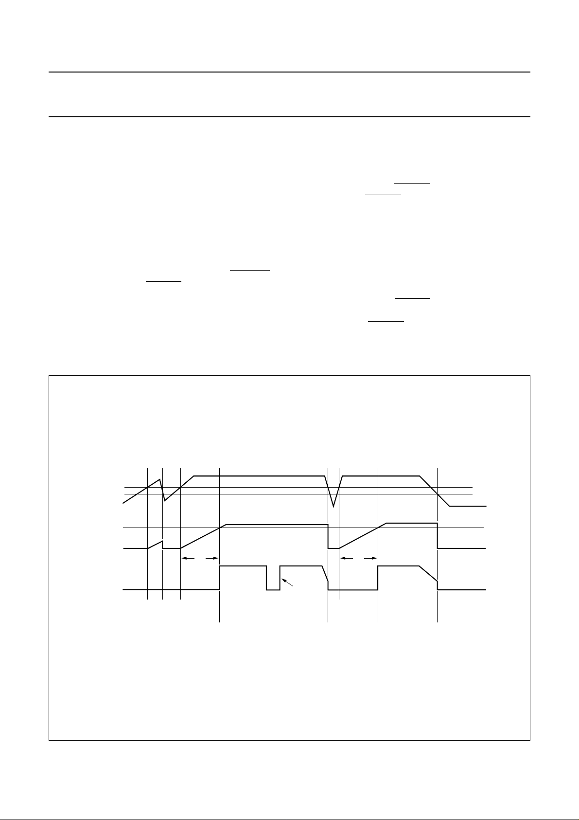
CTIVATION SEQUENCE
A
Figure 4 shows the activation sequence. When the card is
inactive, VCC, CLK, RST and I/O are LOW, with
low-impedance with respect to ground. The DC-to-DC
converter is stopped. SIMI/O is pulled HIGH at V
20 kΩ pull-up resistor. When all conditions are met (supply
voltage, card present, no hardware problems), the
microcontroller may initiate an activation sequence by
setting bit START to logic 1 (t0) via the I2C-bus:
1. The DC-to-DC converter is started (t1).
2. VCC starts rising from 0 to 3 or to 5 V according to
3 V/5 VN control bit with a controlled rise time of
0.17 V/µs typically (t2).
3. I/O buffer is enabled in reception mode (t3).
4. CLK is sent to the card reader with RST = LOW, and
the count of 45000 CLK pulses is started (t4=t
5. If a start bit is detected on I/O, the clock counter is
stopped with RST = LOW. If not, RST = HIGH, and a
new count of 45000 CLK pulses is started (t5).
may be chosen to be
CLK
depending on bit DT/DFN.
DDI
via the
).
act
TDA8003TS
If a start bit is detected on I/O and the clock counter is
stopped with RST = HIGH, the card session may continue.
If not, bit MUTE is set in the status register and
pulled LOW. The microcontroller may initiate a
deactivation sequence by setting bit START to logic 0.
If a start bit is detected during the 200 first CLK pulses of
each count slot, then it will not be taken into account. If a
start bit is detected during 200 and 352 CLK pulses of
each slot, then bit EARLY is set in the status register and
SIMERR is pulled LOW. The microcontroller may initiate a
deactivation sequence by setting bit START to logic 0.
The sequencer is clocked by1⁄64f
which leads to a time
osc
interval T of 25 µs typically. Thus t1=0to1⁄64T;
t2=t1+3⁄2T; t3=t1+7⁄2T; t4=t1+ 4T and t5 depends on
the SIMCLK frequency.
D
EACTIVATION SEQUENCE
Figure 5 shows the deactivation sequence. When the
session is completed, the microcontroller sets bit START
to logic 0. The circuit will execute an automatic
deactivation sequence:
1. Card reset, RST falls to LOW (t10).
2. CLK is stopped (t11).
3. I/O falls to LOW (t12).
4. VCC falls to 0 V with typically 0.17 V/µs slew rate (t13).
The deactivation is completed when VCC reaches
0.4 V (tde).
5. The DC-to-DC converter is stopped and CLK, RST,
VCC and I/O become low-impedance with respect to
PGND (t14).
t10<1⁄64T; t11=t10+1⁄2T; t12=t10+ T; t13=t12+5µs
and t14=t10+ 4T.
SIMERR is
1998 Oct 15 10
Page 11

Philips Semiconductors Preliminary specification
I2C-bus SIM card interface
handbook, full pagewidth
START
V
CC
I/O
CLK
RST
SIMI/O
t0, t1t
2
3
t4 (= t
)t
act
the 200 first CLK pulses are masked
TDA8003TS
MGR437
t
5
Answer To Reset (ATR) begin
handbook, full pagewidth
START
RST
CLK
I/O
V
CC
Fig.4 Activation sequence.
t
10t11
t
13
t
12
t
t
14
de
MGR438
Fig.5 Deactivation sequence.
1998 Oct 15 11
Page 12

Philips Semiconductors Preliminary specification
I2C-bus SIM card interface
Protections
The following main hardware fault conditions are
monitored by the circuit:
• Short-circuits between VCC and other contacts
• Card take-off during transaction
• Supply drop-out.
When one of these problems is detected during a card
session, the security logic block pulls SIMERR to LOW, in
order to warn the microcontroller and initiates an automatic
deactivation of the contacts (see Fig.6).
I/O circuitry
The Idle state is realized by both I/O and SIMI/O being
pulled HIGH (via a 10 kΩ pull-up resistor from I/O to V
and via a 20 kΩ pull-up resistor from SIMI/O to V
I/O is referenced to VCC and SIMI/O to V
operation with VCC≠ VDD≠ V
DDI
.
, thus allowing
DDI
DDI
CC
.
TDA8003TS
When configuration bit I/OEN is logic 0, then
I/O and SIMI/O are independent, which allows
parallelization of several TDA8003TS with only one I/O
line on the microcontroller side (up to 4 different I
addresses).
When bit I/OEN is logic 1, then the data transmission
between I/O and SIMI/O is enabled.
The first side on which a falling edge occurs becomes the
master. An anti-latch circuit disables the detection of falling
edges on the other side, which becomes a slave.
After a delay time td (<500 ns) on the falling edge, the
N transistor on the slave side is turned on, thus
transmitting the logic 0 present on the master side.
When the master goes back to logic 1, the P transistor on
the slave side is turned on during td, and then both sides
return to their Idle states.
The maximum frequency on these lines is 1 MHz.
2
C-bus
handbook, full pagewidth
START
SIMERR
RST
CLK
I/O
V
CC
status readout
MGR439
Fig.6 Emergency deactivation.
1998 Oct 15 12
Page 13

Philips Semiconductors Preliminary specification
I2C-bus SIM card interface
TDA8003TS
LIMITING VALUES
In accordance with the Absolute Maximum Rating System (IEC 134).
SYMBOL PARAMETER CONDITIONS MIN. MAX. UNIT
V
V
V
V
DDP
DDS
DDI
i(n)
power supply voltage −0.5 +6.5 V
signal supply voltage −0.5 +6.5 V
interface signal supply voltage −0.5 +6.5 V
input voltage
on pins 1, 17, 21 and 24 −0.5 +6.5 V
on pins 15, 16, 22 and 23 −0.5 V
DDS
+ 0.5 V
on pins 19 and 20 −0.5 +6.5 V
on pins 9, 11 and 13 −0.5 V
+ 0.5 V
CC
on pin 12 −0.5 +6.5 V
on pin 8 −0.5 +7.5 V
on pins 2, 4, 6 and 7 −0.5 V
I
i(n)
DC input current
VUP
+ 0.5 V
on pins 1, 17, 19, 20, 21, 22, 23 and 24 −5+5mA
on pin 15 −5 +10 mA
I
i/o(n)
DC input/output current
on pins 2, 4, 6, 7 and 8 −40 +40 mA
on pin 16 −5+5mA
P
tot
T
j
T
stg
V
esd(n)
continuous total power dissipation T
= −40 to +85 °C − 230 mW
amb
operating junction temperature − 125 °C
IC storage temperature −55 +150 °C
electrostatic discharge voltage
on pins 9, 11, 12, 13 and 16 −6+6kV
on any other pin −2+2kV
HANDLING
Inputs and outputs are protected against electrostatic discharge in normal handling. However, to be totally safe, it is
desirable to take normal precautions appropriate to handle Metal Oxide Semiconductor (MOS) devices.
THERMAL CHARACTERISTICS
SYMBOL PARAMETER CONDITIONS VALUE UNIT
R
th(j-a)
thermal resistance from junction to ambient in free air 102 K/W
1998 Oct 15 13
Page 14

Philips Semiconductors Preliminary specification
I2C-bus SIM card interface
TDA8003TS
CHARACTERISTICS
V
= 3.3 V; V
DD
= 1.5 V; f
DDI
SIMCLK
= 13 MHz; f
= 3.25 MHz; T
CLK
=25°C; unless otherwise specified.
amb
SYMBOL PARAMETER CONDITIONS MIN. TYP. MAX. UNIT
Supplies
V
DD
I
DD
supply voltage on pins V
and V
DDP
supply current on pins V
and V
DDP
DDS
DDS
Off mode −−2µA
inactive mode −−50 µA
Power-down mode; V
CC
=5V;
2.5 − 6.0 V
−−500 µA
ICC= 100 µA; SIMCLK connected
to SGND or V
active mode; V
active mode; V
; CLK is stopped
DDI
=3V; ICC=6mA −−18 mA
CC
CC
=5V;
−−50 mA
ICC=10mA
active mode; V
=5V; VCC=3V;
DD
−−10 mA
ICC=6mA
active mode; V
=5V; VCC=5V;
DD
−−30 mA
ICC=10mA
V
DDI
I
DDI
V
th(VDD)
V
hys
V
th(DEL)
V
DEL
I
ch(DEL)
I
dch(DEL)
t
W
interface signal supply voltage 1.5 − 6V
interface signals supply
current
threshold voltage on V
hysteresis voltage on V
DD
th(VDD)
SIMCLK connected to
PGND or V
f
SIMCLK
DDI
= 13 MHz; V
= 1.5 V −−120 µA
DDI
−−2µA
falling edge 2 − 2.3 V
40 − 200 mV
threshold voltage on pin DEL − 1.38 − V
voltage on pin DEL −−VDDV
charge current on pin DEL −0.5 −1 −2.5 µA
discharge current on pin DEL V
alarm pulse width C
DEL=VDD
=10nF 15 − 25 ms
DEL
0.5 −− mA
Pin SIMCLK
f
i(SIMCLK)
t
f
t
r
V
IL
V
IH
I
L
clock input frequency 0 − 20 MHz
fall time −−1µs
rise time −−1µs
LOW-level input voltage 0 − 0.3V
HIGH-level input voltage 0.7V
DDI
− V
DDI
DDI
V
+ 0.3 V
leakage current −−±3µA
DC-to-DC converter
1
V
⁄2f
VUP
osc
oscillator frequency 1 − 1.5 MHz
voltage on pin VUP 5 V card − 6.0 − V
3 V card − 4.5 − V
1998 Oct 15 14
Page 15

Philips Semiconductors Preliminary specification
I2C-bus SIM card interface
TDA8003TS
SYMBOL PARAMETER CONDITIONS MIN. TYP. MAX. UNIT
Pin SDA (open-drain)
V
IL
V
IH
I
LH
I
IL
V
OL
LOW-level input voltage −0.3 − +0.3V
HIGH-level input voltage 0.7V
− 6V
DDI
HIGH-level leakage current −−1µA
LOW-level input current depends on the pull-up resistor −−−µA
LOW-level output voltage IOL=3mA −−0.3 V
DDI
V
Pin SCL (open-drain)
V
IL
V
IH
I
LI
Pin
SIMERR (100 kΩ pull-up resistor to V
V
OL
V
OH
Pins SAD0, SAD1 and
V
IL
V
IH
I
LI
LOW-level input voltage −0.3 − +0.3V
HIGH-level input voltage 0.7V
input leakage current −−1µA
LOW-level output voltage IOL<1mA −−0.3V
HIGH-level output voltage IOH< −1 µA 0.7V
PWROFF
LOW-level input voltage 0 − 0.3V
HIGH-level input voltage 0.7V
input leakage current −−±1µA
DDI
− 6V
DDI
)
DDI
−− V
DDI
DDI
− V
DDI
DDI
DDI
+ 0.3 V
V
V
V
Pin RST
V
O
I
O
V
OL
V
OH
t
f
t
r
output voltage inactive mode; IO=1mA −0.3 − +0.4 V
output current inactive mode; pin RST grounded −−−1mA
LOW-level output voltage IOL= 200 µA −0.2 − +0.3 V
HIGH-level output voltage IOH< −200 µAV
− 0.5 − VCC+ 0.2 V
CC
fall time CL=30pF −−0.5 µs
rise time CL=30pF −−0.5 µs
Pin CLK
V
O
I
O
V
OL
V
OH
t
f
t
r
f
clk
output voltage inactive mode; IO=1mA −0.3 − +0.4 V
output current inactive mode; pin CLK grounded −−−1mA
LOW-level output voltage IOL= 200 µA −0.2 − +0.3 V
HIGH-level output voltage IOH= −200 µAV
− 0.5 − VCC+ 0.2 V
CC
fall time CL=30pF −−8ns
rise time CL=30pF −−8ns
clock frequency 1 MHz power-down configuration 1 − 1.5 MHz
regular activity 0 − 10 MHz
δ duty factor CL=30pF 45 − 55 %
1998 Oct 15 15
Page 16

Philips Semiconductors Preliminary specification
I2C-bus SIM card interface
TDA8003TS
SYMBOL PARAMETER CONDITIONS MIN. TYP. MAX. UNIT
Pin V
CC
V
O
output voltage inactive mode; IO=1mA −−0.4 V
active mode; 5 V card; no load 4.85 5.10 5.40 V
active mode; 3 V card; no load 2.8 3.05 3.22 V
active mode; with 200 nF capacitor;
including static load (up to 20 mA)
and dynamic current pulses;
I
= 200 mA, f
max
max
= 5 MHz;
duration <400 ns
5 V card; 40 nAs pulses 4.60 − 5.40 V
3 V card; 24 nAs pulses 2.75 − 3.22 V
I
O
SR slew rate on V
output current inactive mode; pin VCC grounded −−−1mA
V
=5or3V; VDD= 2.5 V −−15 mA
CC
=5or3V; VDD= 5.5 V −−40 mA
V
CC
(rise and fall) C
CC
= 300 nF 0.05 0.17 0.25 V/µs
L(max)
Pin I/O
V
O
I
O
V
OL
V
OH
V
IL
V
IH
I
LIH
output voltage inactive mode; IO=1mA −−0.4 V
output current inactive mode; pin I/O grounded −−−1mA
LOW-level output voltage IOL=1mA −0.2 − +0.3 V
HIGH-level output voltage +25 < IOH< −25 µA 0.8V
− VCC+ 0.2 V
CC
LOW-level input voltage −0.3 − +0.8 V
HIGH-level input voltage 1.5 − VCC+ 0.3 V
HIGH-level input leakage
−−10 µA
current
I
IL
t
t(DI)
t
t(DO)
t
d
R
pu(int)
LOW-level input current −−−600 µA
data input transition time CL=30pF −−1µs
data output transition time CL=30pF −−0.5 µs
delay time on falling edge −−500 ns
internal pull-up resistance
between pins I/O and V
CC
8 − 13 kΩ
Pin SIMI/O
V
V
V
V
I
OL
OH
IL
IH
LIH
LOW-level output voltage IOL=1mA −0.2 − +0.3 V
HIGH-level output voltage with internal 20 kΩ pull-up resistor
to V
; IO=10µA
DDI
LOW-level input voltage −0.3 − +0.3V
HIGH-level input voltage 0.7V
HIGH-level input leakage
V
− 0.3 − V
DDI
DDI
− V
DDI
DDI
+ 0.2 V
DDI
+ 0.3 V
−−10 µA
V
current
I
IL
t
t(DI)
LOW-level input current with internal 20 kΩ pull-up resistor
to V
; VI=0V
DDI
−− µA
V
–
DDI
--------------10kΩ
data input transition time CL=30pF −−1µs
1998 Oct 15 16
Page 17

Philips Semiconductors Preliminary specification
I2C-bus SIM card interface
TDA8003TS
SYMBOL PARAMETER CONDITIONS MIN. TYP. MAX. UNIT
t
t(DO)
t
d
R
pu(int)
data output transition time CL=30pF −−0.5 µs
delay time on falling edge −−500 ns
internal pull-up resistance
16 − 26 kΩ
between pins SIMI/O
and V
DDI
Pin
PRES
V
IL
V
IH
I
IL
I
IH
LOW-level input voltage −0.3 − +0.3V
HIGH-level input voltage 0.7V
− VDD+ 0.3 V
DD
LOW-level input current −−5µA
HIGH-level input current −−−5µA
DD
V
Timing
t
act
t
de
activation time −−150 µs
deactivation time −−120 µs
1998 Oct 15 17
Page 18

This text is here in white to force landscape pages to be rotated correctly when browsing through the pdf in the Acrobat reader.This text is here in
_white to force landscape pages to be rotated correctly when browsing through the pdf in the Acrobat reader.This text is here inThis text is here in
white to force landscape pages to be rotated correctly when browsing through the pdf in the Acrobat reader. white to force landscape pages to be ...
1998 Oct 15 18
handbook, full pagewidth
+1.5 to +6 V
APPLICATION INFORMATION
Philips Semiconductors Preliminary specification
I
2
C-bus SIM card interface
CARD READER
C4 C8
C3 C7
C2 C6
C1 C5
C5I
C6I
C7I
C8I
100 nF
0 Ω
+1.5 V+3.3 V
2.2
µF
100 nF
C1I
C2I
C3I
C4I
K1
(1)
K2
100 nF
+3.3 V
PWROFF
100 nF
PGND
V
100
nF
SGND
1
S1
2
3
S3
4
DDP
5
S4
6
TDA8003TS
S2
7
VUP
8
I/O
9
10
CLK
11
V
CC
12 13
100 nF 100 nF
24
23
22
21
20
19
18
17
16
15
14
SIMCLK
SAD1
SAD0
SIMERR
SCL
SDA
V
DDI
SIMI/O
PRES
DEL
V
DDS
RST
+3.3 V
100 nF
10
nF
+1.5 V
+1.5 V
V
P0-0
P0-1
P0-2
P0-3
P0-4
P0-5
P0-6
P0-7
PSEN
P2-7
P2-6
P2-5
P2-4
P2-3
P2-2
P2-1
P2-0
CC
EA
ALE
40
39
38
37
36
35
34
33
32
31
30
29
28
MICROCONTROLLER
27
26
25
24
23
22
P1-0
1
P1-1
2
P1-2
3
P1-3
4
P1-4
5
P1-5
6
P1-6
7
P1-7
8
RST
9
P3-0
10
P3-1
11
P3-2
12
P3-3
13
P3-4
14
P3-5
15
P3-6
16
P3-7
17
XTAL2
18
XTAL1
19
V
SS
2021
1.5 to 6 kΩ1.5 to 6 kΩ
+1.5 V
14.74 MHz
33 pF
10 µF
33
pF
TDA8003TS
(1) The switch is normally closed when the card is not present.
MGR440
Fig.7 Application diagram.
Page 19

Philips Semiconductors Preliminary specification
I2C-bus SIM card interface
PACKAGE OUTLINE
SSOP24: plastic shrink small outline package; 24 leads; body width 5.3 mm
D
c
y
Z
24 13
TDA8003TS
SOT340-1
E
H
E
A
X
v M
A
pin 1 index
112
w M
b
e
DIMENSIONS (mm are the original dimensions)
mm
A
max.
2.0
0.21
0.05
1.80
1.65
0.25
b
3
p
0.38
0.25
UNIT A1A2A
Note
1. Plastic or metal protrusions of 0.20 mm maximum per side are not included.
p
cD
0.20
8.4
0.09
8.0
0 2.5 5 mm
scale
(1)E(1) (1)
eHELLpQZywv θ
5.4
0.65 1.25
5.2
7.9
7.6
Q
A
2
A
1
detail X
1.03
0.9
0.63
0.7
(A )
L
p
L
A
3
θ
0.13 0.10.2
0.8
0.4
o
8
o
0
OUTLINE
VERSION
SOT340-1 MO-150AG
IEC JEDEC EIAJ
REFERENCES
1998 Oct 15 19
EUROPEAN
PROJECTION
ISSUE DATE
93-09-08
95-02-04
Page 20

Philips Semiconductors Preliminary specification
I2C-bus SIM card interface
SOLDERING
Introduction
There is no soldering method that is ideal for all IC
packages. Wave soldering is often preferred when
through-hole and surface mounted components are mixed
on one printed-circuit board. However, wave soldering is
not always suitable for surface mounted ICs, or for
printed-circuits with high population densities. In these
situations reflow soldering is often used.
This text gives a very brief insight to a complex technology.
A more in-depth account of soldering ICs can be found in
our
“Data Handbook IC26; Integrated Circuit Packages”
(order code 9398 652 90011).
Reflow soldering
Reflow soldering techniques are suitable for all SSOP
packages.
Reflow soldering requires solder paste (a suspension of
fine solder particles, flux and binding agent) to be applied
to the printed-circuit board by screen printing, stencilling or
pressure-syringe dispensing before package placement.
Several techniques exist for reflowing; for example,
thermal conduction by heated belt. Dwell times vary
between 50 and 300 seconds depending on heating
method. Typical reflow temperatures range from
215 to 250 °C.
Preheating is necessary to dry the paste and evaporate
the binding agent. Preheating duration: 45 minutes at
45 °C.
Wave soldering
Wave soldering is not recommended for SSOP packages.
This is because of the likelihood of solder bridging due to
closely-spaced leads and the possibility of incomplete
solder penetration in multi-lead devices.
TDA8003TS
If wave soldering cannot be avoided, the following
conditions must be observed:
• A double-wave (a turbulent wave with high upward
pressure followed by a smooth laminar wave)
soldering technique should be used.
• The longitudinal axis of the package footprint must
be parallel to the solder flow and must incorporate
solder thieves at the downstream end.
Even with these conditions, only consider wave
soldering SSOP packages that have a body width of
4.4 mm, that is SSOP16 (SOT369-1) or
SSOP20 (SOT266-1).
During placement and before soldering, the package must
be fixed with a droplet of adhesive. The adhesive can be
applied by screen printing, pin transfer or syringe
dispensing. The package can be soldered after the
adhesive is cured.
Maximum permissible solder temperature is 260 °C, and
maximum duration of package immersion in solder is
10 seconds, if cooled to less than 150 °C within
6 seconds. Typical dwell time is 4 seconds at 250 °C.
A mildly-activated flux will eliminate the need for removal
of corrosive residues in most applications.
Repairing soldered joints
Fix the component by first soldering two diagonallyopposite end leads. Use only a low voltage soldering iron
(less than 24 V) applied to the flat part of the lead. Contact
time must be limited to 10 seconds at up to 300 °C. When
using a dedicated tool, all other leads can be soldered in
one operation within 2 to 5 seconds between
270 and 320 °C.
1998 Oct 15 20
Page 21

Philips Semiconductors Preliminary specification
I2C-bus SIM card interface
DEFINITIONS
Data sheet status
Objective specification This data sheet contains target or goal specifications for product development.
Preliminary specification This data sheet contains preliminary data; supplementary data may be published later.
Product specification This data sheet contains final product specifications.
Limiting values
Limiting values given are in accordance with the Absolute Maximum Rating System (IEC 134). Stress above one or
more of the limiting values may cause permanent damage to the device. These are stress ratings only and operation
of the device at these or at any other conditions above those given in the Characteristics sections of the specification
is not implied. Exposure to limiting values for extended periods may affect device reliability.
Application information
Where application information is given, it is advisory and does not form part of the specification.
LIFE SUPPORT APPLICATIONS
These products are not designed for use in life support appliances, devices, or systems where malfunction of these
products can reasonably be expected to result in personal injury. Philips customers using or selling these products for
use in such applications do so at their own risk and agree to fully indemnify Philips for any damages resulting from such
improper use or sale.
TDA8003TS
PURCHASE OF PHILIPS I
Purchase of Philips I
components in the I2C system provided the system conforms to the I2C specification defined by
Philips. This specification can be ordered using the code 9398 393 40011.
2
C COMPONENTS
2
C components conveys a license under the Philips’ I2C patent to use the
1998 Oct 15 21
Page 22

Philips Semiconductors Preliminary specification
I2C-bus SIM card interface
TDA8003TS
NOTES
1998 Oct 15 22
Page 23

Philips Semiconductors Preliminary specification
I2C-bus SIM card interface
TDA8003TS
NOTES
1998 Oct 15 23
Page 24

Philips Semiconductors – a worldwide company
Argentina: see South America
Australia: 34 Waterloo Road, NORTH RYDE, NSW 2113,
Tel. +61 2 9805 4455, Fax. +61 2 9805 4466
Austria: Computerstr. 6, A-1101 WIEN, P.O. Box 213, Tel. +43 160 1010,
Fax. +43 160 101 1210
Belarus: Hotel Minsk Business Center, Bld. 3, r. 1211, Volodarski Str. 6,
220050 MINSK, Tel. +375 172 200 733, Fax. +375 172 200 773
Belgium: see The Netherlands
Brazil: see South America
Bulgaria: Philips Bulgaria Ltd., Energoproject, 15th floor,
51 James Bourchier Blvd., 1407 SOFIA,
Tel. +359 2 689 211, Fax. +359 2 689 102
Canada: PHILIPS SEMICONDUCTORS/COMPONENTS,
Tel. +1 800 234 7381
China/Hong Kong: 501 Hong Kong Industrial Technology Centre,
72 Tat Chee Avenue, Kowloon Tong, HONG KONG,
Tel. +852 2319 7888, Fax. +852 2319 7700
Colombia: see South America
Czech Republic: see Austria
Denmark: Prags Boulevard 80, PB 1919, DK-2300 COPENHAGEN S,
Tel. +45 32 88 2636, Fax. +45 31 57 0044
Finland: Sinikalliontie 3, FIN-02630 ESPOO,
Tel. +358 9 615800, Fax. +358 9 61580920
France: 51 Rue Carnot, BP317, 92156 SURESNES Cedex,
Tel. +33 1 40 99 6161, Fax. +33 1 40 99 6427
Germany: Hammerbrookstraße 69, D-20097 HAMBURG,
Tel. +49 40 23 53 60, Fax. +49 40 23 536 300
Greece: No. 15, 25th March Street, GR 17778 TAVROS/ATHENS,
Tel. +30 1 4894 339/239, Fax. +30 1 4814 240
Hungary: see Austria
India: Philips INDIA Ltd, Band Box Building, 2nd floor,
254-D, Dr. Annie Besant Road, Worli, MUMBAI 400 025,
Tel. +91 22 493 8541, Fax. +91 22 493 0966
Indonesia: PT Philips Development Corporation, Semiconductors Division,
Gedung Philips, Jl. Buncit Raya Kav.99-100, JAKARTA 12510,
Tel. +62 21 794 0040 ext. 2501, Fax. +62 21 794 0080
Ireland: Newstead, Clonskeagh, DUBLIN 14,
Tel. +353 1 7640 000, Fax. +353 1 7640 200
Israel: RAPAC Electronics, 7 Kehilat Saloniki St, PO Box 18053,
TEL AVIV 61180, Tel. +972 3 645 0444, Fax. +972 3 649 1007
Italy: PHILIPS SEMICONDUCTORS, Piazza IV Novembre 3,
20124 MILANO, Tel. +39 2 6752 2531, Fax. +39 2 6752 2557
Japan: Philips Bldg 13-37, Kohnan 2-chome, Minato-ku,
TOKYO 108-8507, Tel. +81 3 3740 5130, Fax. +81 3 3740 5077
Korea: Philips House, 260-199 Itaewon-dong, Yongsan-ku, SEOUL,
Tel. +82 2 709 1412, Fax. +82 2 709 1415
Malaysia: No. 76 Jalan Universiti, 46200 PETALING JAYA, SELANGOR,
Tel. +60 3 750 5214, Fax. +60 3 757 4880
Mexico: 5900 Gateway East, Suite 200, EL PASO, TEXAS 79905,
Tel. +9-5 800 234 7381
Middle East: see Italy
Netherlands: Postbus 90050, 5600 PB EINDHOVEN, Bldg. VB,
Tel. +31 40 27 82785, Fax. +31 40 27 88399
New Zealand: 2 Wagener Place, C.P.O. Box 1041, AUCKLAND,
Tel. +64 9 849 4160, Fax. +64 9 849 7811
Norway: Box 1, Manglerud 0612, OSLO,
Tel. +47 22 74 8000, Fax. +47 22 74 8341
Pakistan: see Singapore
Philippines: Philips Semiconductors Philippines Inc.,
106 Valero St. Salcedo Village, P.O. Box 2108 MCC, MAKATI,
Metro MANILA, Tel. +63 2 816 6380, Fax. +63 2 817 3474
Poland: Ul. Lukiska 10, PL 04-123 WARSZAWA,
Tel. +48 22 612 2831, Fax. +48 22 612 2327
Portugal: see Spain
Romania: see Italy
Russia: Philips Russia, Ul. Usatcheva 35A, 119048 MOSCOW,
Tel. +7 095 755 6918, Fax. +7 095 755 6919
Singapore: Lorong 1, Toa Payoh, SINGAPORE 319762,
Tel. +65 350 2538, Fax. +65 251 6500
Slovakia: see Austria
Slovenia: see Italy
South Africa: S.A. PHILIPS Pty Ltd., 195-215 Main Road Martindale,
2092 JOHANNESBURG, P.O. Box 7430 Johannesburg 2000,
Tel. +27 11 470 5911, Fax. +27 11 470 5494
South America: Al. Vicente Pinzon, 173, 6th floor,
04547-130 SÃO PAULO, SP, Brazil,
Tel. +55 11 821 2333, Fax. +55 11 821 2382
Spain: Balmes 22, 08007 BARCELONA,
Tel. +34 93 301 6312, Fax. +34 93 301 4107
Sweden: Kottbygatan 7, Akalla, S-16485 STOCKHOLM,
Tel. +46 8 5985 2000, Fax. +46 8 5985 2745
Switzerland: Allmendstrasse 140, CH-8027 ZÜRICH,
Tel. +41 1 488 2741 Fax. +41 1 488 3263
Taiwan: Philips Semiconductors, 6F, No. 96, Chien Kuo N. Rd., Sec. 1,
TAIPEI, Taiwan Tel. +886 2 2134 2865, Fax. +886 2 2134 2874
Thailand: PHILIPS ELECTRONICS (THAILAND) Ltd.,
209/2 Sanpavuth-Bangna Road Prakanong, BANGKOK 10260,
Tel. +66 2 745 4090, Fax. +66 2 398 0793
Turkey: Talatpasa Cad. No. 5, 80640 GÜLTEPE/ISTANBUL,
Tel. +90 212 279 2770, Fax. +90 212 282 6707
Ukraine: PHILIPS UKRAINE, 4 Patrice Lumumba str., Building B, Floor 7,
252042 KIEV, Tel. +380 44 264 2776, Fax. +380 44 268 0461
United Kingdom: Philips Semiconductors Ltd., 276 Bath Road, Hayes,
MIDDLESEX UB3 5BX, Tel. +44 181 730 5000, Fax. +44 181 754 8421
United States: 811 East Arques Avenue, SUNNYVALE, CA 94088-3409,
Tel. +1 800 234 7381
Uruguay: see South America
Vietnam: see Singapore
Yugoslavia: PHILIPS, Trg N. Pasica 5/v, 11000 BEOGRAD,
Tel. +381 11 625 344, Fax.+381 11 635 777
For all other countries apply to: Philips Semiconductors,
International Marketing & Sales Communications, Building BE-p, P.O. Box 218,
5600 MD EINDHOVEN, The Netherlands, Fax. +31 40 27 24825
© Philips Electronics N.V. 1998 SCA60
All rights are reserved. Reproduction in whole or in part is prohibited without the prior written consent of the copyright owner.
The information presented in this document does not form part of any quotation or contract, is believed to be accurate and reliable and may be changed
without notice. No liability will be accepted by the publisher for any consequence of its use. Publication thereof does not convey nor imply any license
under patent- or other industrial or intellectual property rights.
Internet: http://www.semiconductors.philips.com
Printed in The Netherlands 545104/750/01/pp24 Date of release: 1998 Oct 15 Document order number: 9397 750 04004
 Loading...