

Page 1
BASIC FUNCTION AUDIO PROCESSOR
TWO STEREO AND ONE MONO INPUTS
CONTROLLED
MUTE FUNCTION (SOFTWARE AND HARDWARE)
VOLUMECONTROLIN 1dB STEP
FOURSPEAKER ATTENUATORS:
– Independentattenuationcontrol
– Independentmute function
ALL FUNCTIONS PROGRAMMABLE VIA
2
I
CBUS
TDA7433
DESCRIPTION
The TDA7433is a volume, tone (bass and treble)
balance (Left/Right) processor for quality audio
applicationsin car radioand Hi-Fisystems.
Control is accomplished by serial bus microprocessor interface.
The AC signal setting is obtained by resistor networks and switches combined with operational
amplifiers.
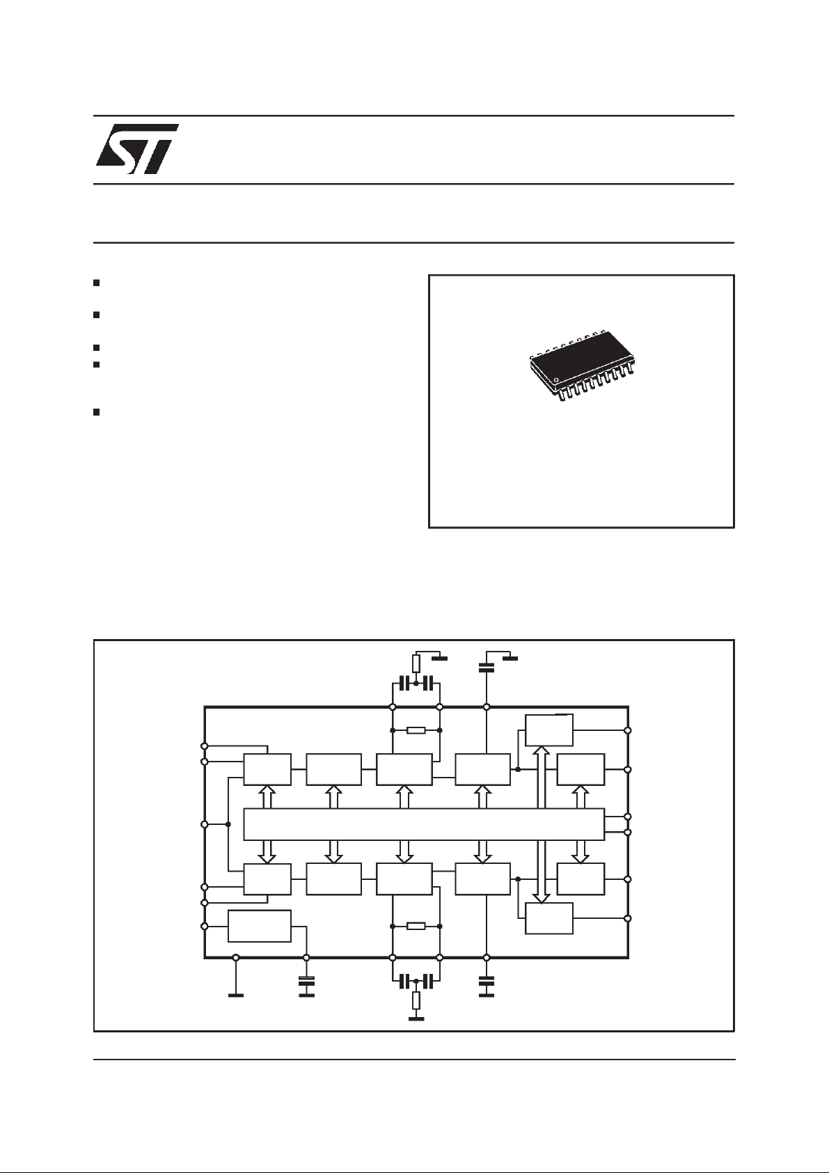
BLOCK DIAGRAM
100nF 100nF
BINL BOUTL TRL
10 9 11
6
IN1_L
3
IN2_L
MONO IN/MUTE
MUX
4
VOL BASS TREBLE
S BUS DECODER + LATCHES
SO20
ORDERING NUMBER: TDA7433D
Thanks to the advanced BIPOLAR/CMOS Technology, the external components have been reduced.
4.7K
2.7nF
SPKR
ATT
SPKR
ATT
16
14
18
19
LEFT FRONT
LEFT REAR
SCL
SDA
November 1999
IN2_R
IN1_R
15
SPKR
ATT
SPKR
ATT
13
D95AU354A
RIGHT FRONT
RIGHT REAR
2
5
17
S
MUX
SUPPLYV
20
GND
VOL BASS TREBLE
18712
BINR BOUTR TRRCREF
100nF 100nF
4.7K
2.7nF
1/10
Page 2
TDA7433
ABSOLUTE MAXIMUM RATINGS
Symbol Parameter Value Unit
V
S
T
amb
T
stg
QUICK REFERENCEDATA
Symbol Parameter Min. Typ. Max. Unit
V
S
V
CL
THD Total Harmonic Distortion (V =1Vrms f = 1kHZ) 0.05 %
S/N Signal to Noise Ratio 102 dB
Sc Channel Separationf = 1kHz 100 dB
Operating Supply Voltage 10.2 V
Operating TemperatureRange -40 to 85 °C
Storage Temperature Range -55 to +150 °C
Supply Voltage 7 9 10.2 V
Max. Input SignalHandling 1.3 1.6 Vrms
Volume Control1dB step -79 +32 dB
Bass Control2dB step -18 +18 dB
Treble Control2dB step -14 +14 dB
Speaker Attenuators -37.5 0 dB
Mute Attenuation 100 dB
PIN CONNECTION(Top View)
MONO IN/MUTE
BOUT_R
BOUT_L TRR
CREF
IN2_R
IN2_L
2
3
4
IN1_R
IN1_L
5
6
7
BIN_R
8
9
BIN_L TRL
10
D95AU355A
20
19
18
17
16
15
14
13
12
11
GND1
SDA
SCL
V
S
OUT_LF
OUT_RF
OUT_LR
OUT_RR
THERMAL DATA
Symbol Parameter Value Unit
Thermal ResistanceJunction-pins Max. 150 °C/W
2/10
R
th j-pins
Page 3
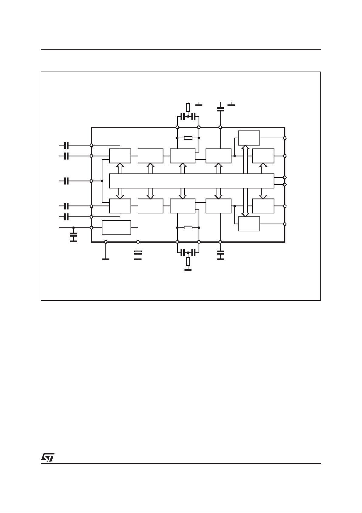
APPLICATIONDIAGRAM
TDA7433
4.7K
100nF 100nF
10 9 11
100nF
IN1_L
6
IN2_L
3
100nF
100nF
MONO/
MUTE
100nF
IN2_R
IN1_R
100nF
9V
V
S
100nF
4
2
5
V
17
S
SUPPLY
20
GND
MUX
MUX
VOL BASS TREBLE
S BUS DECODER+ LATCHES
VOL BASS TREBLE
1 8712
CREF BINR BOUTR TRR
10µF
100nF 100nF
4.7K
2.7nF
TRLBOUTLBINL
2.7nF
SPKR
ATT
SPKR
ATT
SPKR
ATT
SPKR
ATT
16
14
18
19
15
13
D95AU356A
LEFT FRONT
LEFT REAR
SCL
SDA
RIGHT FRONT
RIGHT REAR
3/10
Page 4

TDA7433
ELECTRICALCHARACTERISTICS
=25°C,VS=9V, RL= 10kΩ,Rg=50Ω,
(T
amb
all variablegains = 0dB, f = 1kHz, unlessotherwisespecified.)
Symbol Parameter Test Condition Min. Typ. Max. Unit
INPUT SELECTOR
R
IN
V
CL
S
IN
A
MUTE
V
DC
MUTE AT AM INPUT (*)
V
IL
VOLUME CONTROL
G
MAX
A
MAX
A
step
E
A
E
T
V
DC
BASS CONTROL
B
RANGE
B
CUT
A
Step
R
B
TREBLE CONTROL
C
RANGE
A
step
SPEAKER ATTENUATORS
C
RANGE
A
step
A
MUTE
E
A
V
DC
AUDIO OUTPUTS
V
CLIP
G
OUT
R
L
C
L
R
OUT
VDC DC Voltage Level 3.7 4.0 4.3 V
(*) The mute function can be activatedwithout using the I2C bus by groundingthe AMinput whenAM is notselected. This causes theinput
multiplexer to select the referencevoltage instead ofan input signal.
Input Resistance 70 100 130 kΩ
Clipping Level d≤ 0.3% 1.3 1.6 Vrms
Input Separation 70 100 dB
Input Mute Attenuation 70 95 dB
Mute DC Step 0.2 10 mV
Input Low Voltage AM not selected 0.4 V
Max. Gain Note 2 30.5 32 33.5 dB
Max Attenuation 75 79 83 dB
Step Resolution 0.5 1 1.5 dB
Attenuation Set Error G = +20 to -20dB -1.0 0 +1.0 dB
G = -20 to -60dB -2 2 dB
Tracking Error G = -20 to -60dB 2 dB
DC Steps Adjacent AttenuationSteps,
0.1 4 mV
Range from 0 to -79dB
From 0dB to -79dB 0.5 10 mV
Max. Bassboost 15.5 18 20 dB
Max. Basscut -20 -18 15.5 dB
Step Resolution 1 2 3 dB
Internal Feedback Resistance 48 65 82 kΩ
Control Range ±13 ±14 ±15 dB
Step Resolution 1 2 3 dB
Control Range 36 37.5 39 dB
Step Resolution From 0 to -24dB 0.5 1 1.5 dB
Output MuteAttenuation From 0 to -24dB 70 90 dB
Attenuation Set Error 1 dB
DC Steps Adjacent AttenuationSteps 0.1 4 mV
Clipping Level d = 0.3% 2 2.5 Vrms
Output Gain(fixed) 4 dB
Output LoadResistance AC - connected 3 k
Ω
DC connectedto GND 5
Output LoadCapacitance 10 nF
Output Impedance 30 100 Ω
4/10
Page 5

TDA7433
ELECTRICALCHARACTERISTICS
(continued)
Symbol Parameter Test Condition Min. Typ. Max. Unit
GENERAL
V
S
I
S
Supply Voltage 6 9 10.2 V
Supply Current 5 8 11 mA
PSRR Power SupplyRejection Ratio 65 85 dB
e
NO
Output Noise 20Hz - 20kHz ”A” - weighted
BW = 200Hz - 20kHz,flat
output muted
S/N Signal to Noise Ratio all gains= 0dB; V
d Distortion V
= 1Vrms 0.05 0.15 %
OUT
= 1Vrms 102 dB
O
4
7.0
5.5
20
Sc Channel Separation 70 80 dB
E
T
Total TrackingError AV= 0to -20dB
A
= -20to -60dB
V
0
0
1
2
BUS INPUTS
V
IL
V
IH
I
IN
V
O
Input Low Voltage 1V
Input High Voltage 3 V
Input Current VIN= 0.4V -5 +5 µA
Output Voltage
IO= 1.6mA 0.15 0.4 V
SDA Acknowledge
SOFTWARESPECIFICATION
Interface Protocol
The interfaceprotocol comprises:
– a startcondition(S)
– a chipaddress byte(the LSBbit determinesread /write transmission)
– a subaddressbyte
– a sequenceof data (N-bytes+ acknowledge)
– a stop condition (P)
µ
µV
µV
dB
dB
V
MSB
CHIP ADDRESS
LSB
MSB
SUBADDRESS
LSB MSB
DATA 1...DATA n
LSB
S 1 0 0 0 1 0 1 R/W ACK X X X I A3A2A1A0ACK DATA ACK P
ACK = Acknowledge
S = Start
P = Stop
MAX CLOCK SPEED 500kbits/s
Auto Increment
If bit I inthe subaddressbyte is set to ”1”, the autoincrementof the subaddressis enabled.
5/10
Page 6

TDA7433
SUBADDRESS
(receivemode)
MSB LSB
X X X I A3A2A1A0
0
0
0
0
0
0
0
0
0
0
0
1
1
1
0
0
1
1
0
0
1
I = Autoincrement
X = Notused
DATA BYTESPECIFICATION
X = notrelevant; set to ”1” during testing
Input Selector
MSB LSB
D
D
7
D
6
D
5
D
4
D
3
D
2
0
0
0
0
1
1
0
0
1
1
X
0
1
0
1
Input selector
0
Volume
1
Bass, Treble
0
Speaker attenuator LF
1
Speaker attenuator LR
0
Speaker attenuator RF
1
Speaker attenuator RR
0
D
0
IN2
0
IN1
1
mono IN
0
no inputselected
1
mute (lowhomic)
X
non-symmetrical bass cut (note1)
symmetrical bass cut
extended bass range
standard bass range±14dB
FUNCTION
FUNCTION
For exampleto select the IN2 inputthe DataByte is: XX X X X 0 1 0.
An additionaldirect mute functionis included in the SpeakerAttenuators.
Note 1: Basscut for very low frequencies.
MSB LSB
D
D
7
0
0
0
0
0
0
0
0
0
0
D
6
0
0
0
0
1
1
1
D
5
0
0
1
1
0
0
1
D
4
0
1
0
1
0
1
0
D
3
D
2
D
1
0
+32dB
+16dB
0dB
-16dB
-32dB
-48dB
-64dB
0
0
0
0
0
0
0
0
1
0
0dB
1
-1dB
0
-2dB
0
0
Note 2:
It is not recommended to use a gain more than 20dB for system performance reason. In general, the max. gain should be limited by
software to the maximum value, which is needed forthe system.
1
1
1
1
-15dB
VOLUME
6/10
Page 7

Bass, Treble
TDA7433
MSB LSB
D
D
D
D
D
D
D
7
6
5
4
3
2
D
1
0
Treble Steps
- 14dB
0
0
0
D4
Input
Selector
0
0
0
0
0
0
0
0
0
0
1
1
1
1
1
1
1
1
1
0
1
0
0
1
0
1
1
1
1
1
1
1
1
1
0
1
0
1
1
0
1
0
0
0
0
0
-12dB
1
-10dB
0
-8dB
1
-6dB
0
-4dB
1
-2dB
0
0dB
1
0dB
1
+2dB
0
+4dB
1
+6dB
0
+8dB
1
+10dB
0
+12dB
1
+14dB
0
Bass Steps
0
0
1
1
1
1
1
1
1
1
1
1
1
1
1
1
1
1
0
0
For example 12dB Treble and -8dB Bass give the following DATA BYTE:0 01110 0
0
0
0
0
0
0
0
0
0
0
0
0
0
1
0
1
0
1
0
1
0
1
1
1
1
1
1
1
1
0
1
0
1
0
1
0
1
0
1
0
1
0
0
1
0
0
1
1
1
0
0
1
0
0
1
1
1
1
1
0
1
1
0
0
0
1
1
0
1
1
0
0
0
0
0
1
0
1
0
0
-18dB
-16dB
-14dB
-12dB
-10dB
-8dB
-6dB
-4dB
-2dB
0dB
0dB
+2dB
+4dB
+6dB
+8dB
+10dB
+12dB
+14dB
+16dB
+18dB
normal
range
14dB
±
FUNCTION
Speaker Attenuators
MSB LSB SPEAKER ATTENUATOR
D
7
X
X
X
X
X
X
X
X
X
X
X
D
6
X
X
X
X
X
X
X
X
X
X
X
D
5
0
0
0
0
0
0
0
0
0
0
1
D
4
0
0
1
1
1
1
1
1
1
1
X
D
3
0
0
:
1
1
1
1
1
1
1
1
X
D
2
0
0
D
1
0
0
D
0
0dB
0
-1dB
1
:
-24dB
0
0
0
0
1
1
1
1
X
0
0
1
1
0
0
1
1
X
0
1
0
1
0
1
0
1
X
-25.5dB
-27dB
-28.5dB
-30dB
-32dB
-34.5dB
-37.5dB
Speaker Mute
LF,LR,RF,RR
7/10
Page 8

TDA7433
Functional Description
The input selectoris able to select 2 stereo inputs
and 1 mono input (AM). The inputsare DC biased
with 100kΩ resistorsto the internal reference voltage of 3V. The mono input can be used additionally as hardware mute pin. If this pin is pulled to
ground by an externaltransistor and AM is not selected, the input selector mutes the input (reference voltage selected). The AM part is considered to be switched OFF. If the output of the AM
part is not high ohmic in this condition, a series
resistor of about 20kΩ hasto be foreseen.
The volume control can be programmed from a
gain of +32dB to an attenuation of -79dB in 1dB
steps. The maximum gain should be kept as low
as possiblefor system performancereason. It has
to be limited by software to the absolute necessary system gain, dependingon the signal source
level and the power amplifier gain.
The bass control acts in a range from +18dB to 18dB in 2dB steps. The filter response is deter-
mined by the external filter components. An extensive simulation softwareis available in order to
supportthe design of the bass filter response with
differentfilter configurations.
The extended bass boost range of +18dB allows
the implementationof the software loudness function by additionalbass and treble boost.
The treble control acts in a range of ±14dB in 2dB
steps. The external capacitor determines with the
internal resistor of 50KΩthe corner frequency of
the treble response.
The four speaker attenuatorscan be controlledindependentlyfrom 0 to -37.5dB, which allows the
implementation of balance and fader a the four
speaker system. The attenuation steps size is 1
db from 0 to -24dB and increases non linearly up
to the maximum attenuationof 37.5dB. A special
mute bit forces the speaker attenuator into the
muteposition.
All 4 outputs are low distortion push pull outputs,
able to drive a load of 3kΩ.
8/10
Page 9

TDA7433
DIM.
MIN. TYP. MAX. MIN. TYP. MAX.
A 2.35 2.65 0.093 0.104
A1 0.1 0.3 0.004 0.012
B 0.33 0.51 0.013 0.020
C 0.23 0.32 0.009
D 12.6 13 0.496 0.512
E 7.4 7.6 0.291 0.299
e 1.27 0.050
H 10 10.65 0.394 0.419
h 0.25 0.75 0.010 0.030
L 0.4 1.27 0.016 0.050
K0°(min.)8° (max.)
mm inch
0.013
OUTLINE AND
MECHANICAL DATA
SO20
B
e
D
1120
110
L
hx45°
A
K
A1
C
H
E
SO20MEC
9/10
Page 10

TDA7433
Information furnished is believed to be accurate and reliable. However, STMicroelectronics assumes no responsibility for the consequences
of use of such information nor for any infringement of patents or other rights of third parties which may result from its use. No license is
granted by implication or otherwise under any patent or patent rights of STMicroelectronics. Specification mentioned in this publication are
subject to change without notice. This publication supersedes and replaces all information previously supplied. STMicroelectronics products
are not authorized for use as critical components in life support devices or systems without express written approval of STMicroelectronics.
The ST logo is a registered trademark of STMicroelectronics
1999 STMicroelectronics – Printed in Italy– All Rights Reserved
STMicroelectronics GROUPOF COMPANIES
Australia - Brazil - China - Finland - France - Germany - HongKong - India - Italy - Japan - Malaysia - Malta - Morocco -
Singapore - Spain - Sweden - Switzerland - United Kingdom - U.S.A.
http://www.st.com
10/10
 Loading...