

Page 1
3 BAND EQUALIZER AUDIO PROCESSOR
■
3 STEREO INPUTS
■ AUXILIARY MONO INPUT
■
INPUT ATTENUATION CONTROL IN 0.5dB
STEP
■ TREBLE MIDDLE AND BASS CONTROL
■
FOUR SPEAKERS ATTENUATORS:
- 4 INDEPENDENT SPEAKERS CONTROL IN
1dB STEPS FOR BALANCE FACILITY
- INDEPENDENT MUTE FUNCTION
■
SUBWOOFER OUTPUT (L+R)CONTROLLED
IN 1dB STEP INPUTS
■
ALL FUNCTIONS PROGRAMMABLE VIA
SERIAL BUS
DESCRIPTION
The TDA7429L is volume tone (bass middle and treble) balance (Left/Right) processors for quality audio
applications in TV and Hi-Fi systems, providing also
TDA7429L
WITH SUBWOOFER CONTROL
SDIP42
ORDERING NUMBER: TDA7429L
an additional subwoofer control.
The AC signal setting is obtained by resistor networks
and switches combined with operational amplifiers.
Thanks to the used BIPOLAR/CMOS Technology,
Low Distortion, Low Noise and DC stepping are obtained.
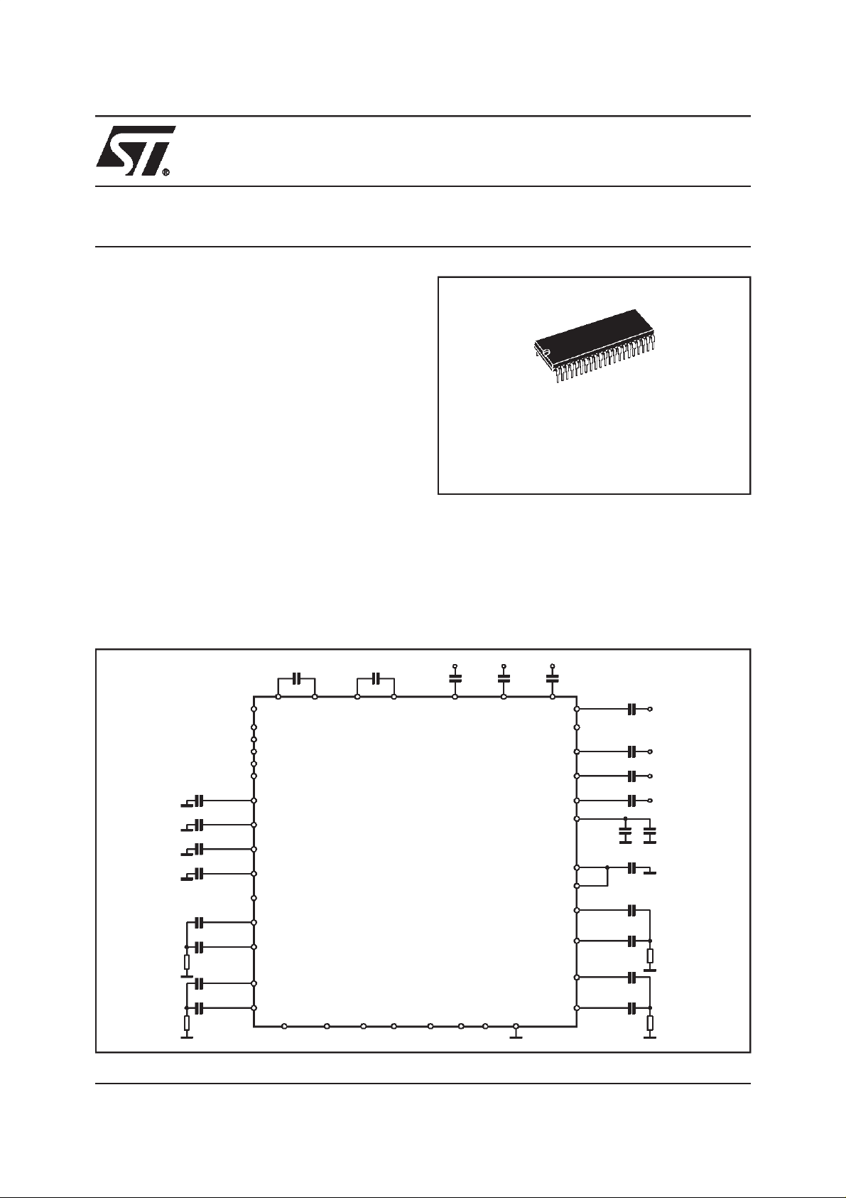
Figure 1. Test Circuit
L+R OUTPUT 9
100nF
100nF
TREBLE_R
5.6nF
TREBLE_L
100nF
MONITOR_R
22nF
MIDDLE_LO
18nF
22nF
18nF
MIDDLE_LI
MIDDLE_RO
MIDDLE_RI
2.7K
2.7K
2.2µF
14
N.C.
1
N.C.
2
N.C.
3
N.C.
4
N.C.
7
LP
5
LP1
6
23
24
37
19
20
21
22
AUXOUT_L AUXOUT_R L_OUT R_OUT
BASSO_LVAR_RBASSO_R
13 12 11
32 31 30 29 28 27 26 25
2.2µF
VAR_L
0.47µF
MONO INPUT
DIG_GND SCL SDA AGND
0.47µF
R_IN3
10
40 39
0.47µF
R_IN2
38
35
34
33
42
41
8
15
16
17
18
R_IN1
MONITOR_L36
L_IN1
L_IN2
L_IN3
V
S
CREF
HP2
BASS_LO
BASS_LI
BASS_RO
BASS_RI
D99AU1029
0.47µF
0.47µF
0.47µF
0.47µF
100nF10µF
22µF
220nF
100nF
100nF
5.6K
100nF
100nF
5.6K
March 2000
1/16
Page 2
TDA7429L
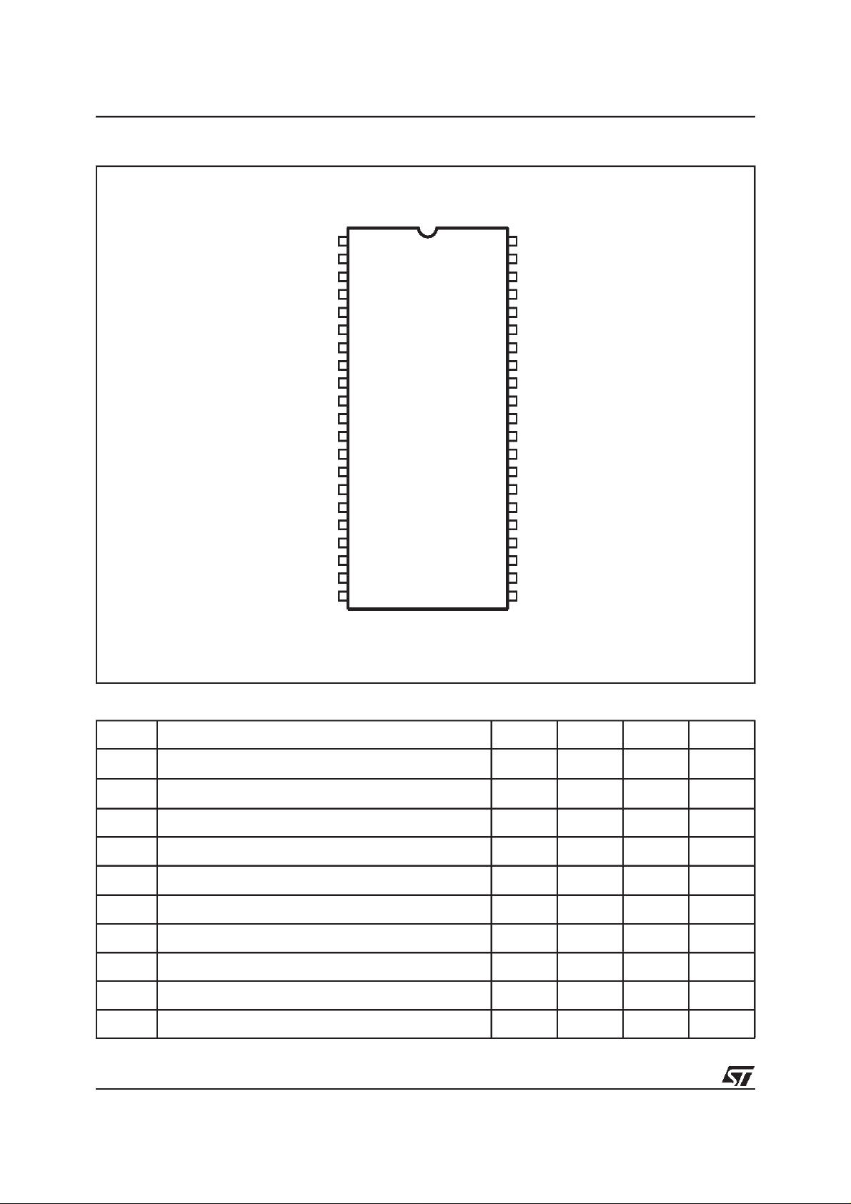
Figure 2. Pin Connection
N.C.
N.C.
N.C.
N.C.
LP
LP1
N.C.
HP2
L+R OUTPUT
MONO INPUT
VAR_L
BASSO_L
VAR_R
BASSO_R
BASS_LO
BASS_LI
BASS_RO
BASS_RI
MIDDLE_LO
MIDDLE_LI
MIDDLE_RO
1
2
3
4
5
6
7
8
9
10
11
12
13
14
15
16
17
18
19
20
21
D99AU1028
42
41
40
39
38
37
36
35
34
33
32
31
30
29
28
27
26
25
24
23
22
V
S
CREF
R_IN3
R_IN2
R_IN1
MONITOR_R
MONITOR_L
L_IN1
L_IN2
L_IN3
AUXOUT_L
AUXOUT_R
L_OUT
R_OUT
DIG_GND
SCL
SDA
AGND
TREBLE_L
TREBLE_R
MIDDLE_RI
Table 1. Quick Reference Data
Symbol Parameter Min. Typ. Max. Unit
V
V
THD Total Harmonic Distortion V = 1Vrms f = 1KHz 0.01 0.1 %
S/N Signal to Noise Ratio V out = 1Vrms (mode = OFF) 106 dB
S
2/16
Supply Voltage 7 9 10.2 V
S
Max. input signal handling 2 Vrms
CL
Channel Separation f = 1KHz 90 dB
C
Treble Control (2db step) -14 +14 dB
Middle Control (2db step) -14 +14 dB
Bass Control (2dB step) -14 +14 dB
Balance Control 1dB step (LCH, RCH) -79 0 dB
Mute Attenuation 100 dB
Page 3

Figure 3. Block Diagram.
AUXOUT_L
32
ATT
SPKR
79dB CONTROL
30
L_OUT
MUTE
SCL
SDA
272628
DIG GND
ATT
SPKR
29
R_OUT
MUTE
AUXOUT_R
31
79dB CONTROL
TDA7429L
D99AU1030
5.6K
2.7K
100nF
100nF
22nF
18nF
5.6nF
100nF
2.2µF
BASSO_L VAR_L
BASS_LO
15 12 11
BASS_LI
MIDDLE_LO
MIDDLE_LI
20 19 16
24
TREBLE_L
LP1
6
30K
-
+
FIX
VAR
ATT
REC
MUTE
79dB CONTROL
FIX
RB
SURR
RM
OFF
3BAND
C BUS DECODER + LATCHES
2
REAR
LPF 1
+
I
BASS
MIDDLE
TREBLE
OFF
TREBLE MIDDLE BASS
L+R
CONTROL
LPF 2
-
+
30K
1314172337
50K
Vref
SUPPLY
MUTE
RM RB
VAR_R
BASSO_R
79dB CONTROL
22 21 18
TREBLE_R
910
L+R OUTPUT
LP
HP2
8
2.2µF
REARIN
100nF
22µF
CREF
AGND
BASS_RO
BASS_RI
100nF 100nF
MIDDLE_RO
18nF 22nF
MIDDLE_RI
5.6nF
0.47µF
5.6K
2.7K
FIX
VAR
ATT
REC
3BAND
FIX
SURR
REAR
OFF
31.5dB
control
36
MONITOR_L
35
0.47µF
L_IN1
50K
S
V
42 25 41 5
31.5dB
control
MONITOR_R
50K
50K
34
33
L_IN2
L_IN3
0.47µF
0.47µF
50K
50K
50K
38
39
40
R_IN3
R_IN2
R_IN1
0.47µF
0.47µF
0.47µF
THE SWITCHES POSITION MATCHES THERESET CONDITION
3/16
Page 4

TDA7429L
Table 2. Thermal Data
Symbol Description Value Unit
R
th j-pins
Thermal Resistance Junction-pins Max.
85 °C/W
Table 3. Absolute Maximum Ratings
Symbol Parameter Value Unit
V
T
T
Operating Supply Voltage 11 V
S
Operating Ambient Temperature -10 to 85 °C
amb
Storage Temperature Range -55 to +150 °C
stg
Table 4. Electrical Characteristics
(refer to the test circuit T
=25°C, VS=9V,RL= 10KΩ,Vin=1V
amb
rms;RG
= 600Ω, all controls flat
(G = 0dB), L+R CTRL = +4dB, MODE = OFF; f = 1KHz unless otherwise specified).
Symbol Parameter Test Condition Min. Typ. Max. Unit
SUPPLY
V
SVR Ripple Rejection L
INPUT STAGE
R
V
C
RANGE
A
VMIN
A
VMAX
A
STEP
BASS CONTROL
Supply Voltage 7 9 10.2 V
S
Supply Current 10 18 26 mA
I
S
CH/RCH out
Input Resistance 35 50 65 KΩ
IN
Clipping Level THD = 0.3% 2 2.5 V
CL
, Mode = OFF 60 80 dB
Control Range 31.5 dB
Min. Attenuation -1 0 1 dB
Max. Attenuation 31 31.5 32 dB
Step Resolution 0.5 1 dB
rms
B
G
STEP
R
Control Range Max. Boost/cut ±11.5 ±14.0 ±16.0 dB
b
Step Resolution 1 2 3 dB
Internal Feedback Resistance 32 44 56 KΩ
B
MIDDLE CONTROL
M
G
STEP
R
Control Range Max. Boost/cut ±11.5 ±14.0 ±16.0 dB
m
Step Resolution 1 2 3 dB
Internal Feedback Resistance 17.5 25 32.5 KΩ
M
TREBLE CONTROL
G
Control Range Max. Boost/cut ±13.0 ±14.0 ±15.0 dB
t
T
STEP
Step Resolution 1 2 3 dB
4/16
Page 5

TDA7429L
Table 4. Electrical Characteristics
(refer to the test circuit T
(G = 0dB), L+R CTRL = +4dB, MODE = OFF; f = 1KHz unless otherwise specified).
Symbol Parameter Test Condition Min. Typ. Max. Unit
CONTROL L+R
=25°C, VS=9V,RL= 10KΩ,Vin=1V
amb
rms;RG
= 600Ω, all controls flat
C
RANGE
S
STEP
Control Range - 11 +4 dB
Step Resolution 0.5 1 1.5 dB
SPEAKER & AUXATTENUATORS
C
RANGE
S
STEP
V
A
MUTE
R
E
Control Range 79 dB
Step Resolution -0.5 1 1.5 dB
Attenuation set error Av= 0 to -20dB -1.5 0 1.5 dB
A
A
= -20 to -79dB -3 0 2 dB
v
DC Steps adjacent att.steps -3 0 3 mV
DC
Output Mute Condition +70 100 dB
Input Impedance 21 30 39 KΩ
VEA
AUDIO OUTPUTS
N
O(OFF)
Output Noise (OFF) Output Mute, Flat
BW = 20Hz to 20KHz
d Distorsion Av=0;Vin=1V
V
R
V
S
OUT
Channel Separation 70 90 dB
C
Clipping Level d = 0.3% 2 2.5 Vrms
OCL
Output Resistance 20 40 70 Ω
OUT
DC Voltage Level 3.8 V
MONITOR OUTPUTS
rms
4
5
µV
µV
0.01 0.1 %
rms
rms
d Distorsion A
V
R
V
S
OUT
Channel Separation 70 90 dB
C
Clipping Level d = 0.3% 2 2.5 Vrms
OCL
Output Resistance 20 50 70 Ω
OUT
DC Voltage Level 4.5 V
BUS INPUTS
V
V
I
V
Input Low Voltage 1V
IL
Input High Voltage 3 V
IH
Input Current -5 +5 mA
IN
Output Voltage SDA
O
Acknowledge
=0;Vin=1V
v
rms
0.01 0.1 %
IO= 1.6mA 0.4 V
5/16
Page 6

TDA7429L
1.0 I2C BUS INTERFACE
Data transmission from microprocessor to the TDA7429L and viceversa takes place through the 2 wires I2C
BUS interface, consisting of the two lines SDA and SCL (pull-up resistors to positive supply voltage must be
connected).
1.1 Data Validity
As shown in fig. 3, the data on the SDA line must be stable during the high period of the clock. TheHIGH and
LOW state of the data line can only change when the clock signal on the SCL line is LOW.
1.2 Start and Stop Conditions
As shown in fig.4 a start condition is a HIGH to LOW transition of the SDA line while SCL is HIGH. The stop
condition is a LOW to HIGH transition of the SDA line while SCL is HIGH.
1.3 Byte Format
Every byte transferred on the SDA linemust contain 8 bits. Each bytemust be followed byan acknowledge bit.
The MSB is transferred first.
1.4 Acknowledge
The master (mP) puts a resistive HIGH level on the SDA line during the acknowledge clock pulse (see fig. 5).
The peripheral (audioprocessor) that acknowledges has to pull-down (LOW) the SDA line during this clock
pulse.
The audioprocessor which has been addressed has to generate an acknowledge after the reception of each
byte, otherwise the SDA lineremains atthe HIGH level during the ninth clock pulse time. Inthis case the master
transmitter can generate the STOP information in order to abort the transfer.
1.5 Transmission without Acknowledge
Avoiding to detect the acknowledge of the audioprocessor, the µP can use a simpler transmission: simply it
waits one clock without checking the slave acknowledging, and sends the new data.
This approach of course is less protected from misworking.
Figure 4. Data validity on the I2Cbus
SDA
SCL
DATA
LINE
STABLE,DAT
VALID
A
CHANGE
DAT
A
ALLOWED
D99AU1031
Figure 5. Timing Diagram of I2C bus
SCL
I2CBUS
SDA
START
D99AU1032
STOP
6/16
Page 7

Figure 6. Acknowledge on the I2C bus
TDA7429L
SCL
SDA
START
1
MSB
23789
D99AU1033
2.0 SOFTWARE SPECIFICATION
2.1 Interface Protocol
The interface protocol comprises:
■
A start condition (S)
■
A chip address byte, containing the TDA7429L address
■
A subaddress bytes
■ A sequence of data (N byte + achnowledge)
■
A stop condition (P)
CHIP ADDRESS
MSB LSB MSB LSB MSB LSB
S 1 0 0 0 0 0 A 0 ACK ACK DATA ACK P
D95AU226A
ACK = Acknowledge S = Start
SUBADDRESS DATA 1 to DATA n
B DATA
P = Stop A = Address B = AutoIncrement
ACKNOWLEDGMENT
FROM RECEIVER
3.0 EXAMPLES
3.1 No Incremental Bus
The TDA7429L receives a start condition, the correct chip address, a subaddress with the MSB = 0 (no incremental bus), N-datas (all these datas concern the subaddress selected), a stop condition.
CHIP ADDRESS
MSB LSB MSB LSB MSB LSB
S 1 0 0 0 0 0 A 0 ACK ACK DATA ACK P
D95AU306
SUBADDRESS DATA
0D3
XXX D2D1D0
3.2 Incremental Bus
The TDA7429L receivesa start condition, the correct chip address, asubaddress with theMSB = 1(incremental
bus): now it is in a loop condition with an autoincrease of the subaddress whereas SUBADDRESS from
”1XXX1010” to ”1XXX1111” of DATA are ignored.The DATA 1 concern thesubaddress sent, and the DATA 2
concern the subaddress sent plus one in the loop etc, and at the end it receivers the stop condition.
CHIP ADDRESS
MSB LSB MSB LSB MSB LSB
S 1 0 0 0 0 0 A 0 ACK ACK DATA ACK P
D95AU307
SUBADDRESS DATA 1 toDATAn
1D3
XXX D2D1D0
7/16
Page 8

TDA7429L
Table 5. Function Selection
The first byte (subaddress)
MSB L SB
D7 D6 D5 D4 D3 D2 D1 D0
1
B
2
X
XX0000INPUT ATTENUATION
BXXX0001CONTROL OUT L+R &
SUBWOOFER
BXXX0010NOTUSED
BXXX0011BASS & NATURAL BASE
BXXX0100MIDDLE & TREBLE
BXXX0101SPEAKER ATTENUATION”L“
BXXX0111AUXATTENUATION”L”
BXXX1000AUXATTENUATION”R”
BXXX1001INPUT MULTIPLEXER, & AUX OUT
SUBADDRESS
<1> B =1 incremental bus; active
<2> X =indifferent 0,1
B =0 no incremental bus;
Table 6. Input Attenuation Selection
MSB LSB INPUT ATTENUATION
D7 D6 D5 D4 D3 D2 D1 D0 0.5 dB STEPS
X 000 0
X 0 0 1 -0.5
X 010 -1
X 0 1 1 -1.5
X 100 -2
X 1 0 1 -2.5
X 110 -3
X 1 1 1 -3.5
4 dB STEPS
X000 0
X001 -4
X010 -8
X011 -12
X100 -16
X101 -20
X110 -24
X111 -28
INPUT ATTENUATION= 0 ~ -31.5dB
D7 D6 D5 D4 D3 D2 D1 D0 L+R OUTPUT SWITCH
X 0 (L+R) OUTPUT PIN ACTIVE
8/16
Page 9

TDA7429L
Table 7. Out & (L+R) & Subwoofer Selection
MSB L SB
D7 D6 D5 D4 D3 D2 D1 D0 SUBWOOFER CONTROL
X 0 0 SUBWOOFER ON
X 0 1 NOT ALLOWED
X 1 0 SUBWOOFER OFF
X 1 1 NOT ALLOWED
OUT
X0VAR
X 1 FIX
L+R CONTROL
X0000 +4
X0001 +3
X0010 +2
X0011 +1
X0100 0
X0101 -1
X0110 -2
X0111 -3
X1000 -4
X1001 -5
X1010 -6
X1011 -7
X1100 -8
X 1 1 0 1 --9
X1110 -10
X1111 -11
Table 8. Bass Selection
MSB LSB BASS
D7 D6 D5 D4 D3 D2 D1 D0 2 dB STEPS
XXX10000 -14
XXX10001 -12
XXX10010 -10
XXX10011 -8
XXX10100 -6
XXX10101 -4
XXX10110 -2
XXX10111 0
XXX11111 0
XXX11110 2
XXX11101 4
XXX11100 6
XXX11011 8
XXX11010 10
XXX11001 12
XXX11000 14
9/16
Page 10

TDA7429L
Table 9. Speaker/Aux Att. R & LSelection
MSB LSB SPEAKER/AUX ATT
D7 D6 D5 D4 D3 D2 D1 D0 1 dB STEPS
X 000 0
X 001 -1
X 010 -2
X 011 -3
X 100 -4
X 101 -5
X 110 -6
X 111 -7
8 dB STEPS
X0000 0
X0001 -8
X0010 -16
X0011 -24
X0100 -32
X0101 -40
X0110 -48
X0111 -56
X1000 -64
X1001 -72
MUTE
X101X
X11XX
Notes: 1. X = INDIFFERENT 0.1
2. SPAEAKER/AUXATTENUATI ON= 0dB to 79dB
10/16
Page 11

Table 10. Middle & Treble Selection
MSB LSB MIDDLE
D7 D6 D5 D4 D3 D2 D1 D0 2 dB STEPS
0000 -14
0001 -12
0010 -10
0011 -8
0100 -6
0101 -4
0110 -2
0111 0
1111 0
1110 2
1101 4
1100 6
1011 8
1010 10
1001 12
1000 14
TREBLE
2 dB STEPS
0000 -14
0001 -12
0010 -10
0011 -8
0100 -6
0101 -4
0110 -2
0111 0
1111 0
1110 2
1101 4
1100 6
1011 8
1010 10
1001 12
1000 14
TDA7429L
11/16
Page 12

TDA7429L
Table 11. Input/recout L & R Selection
MSB L SB
D7 D6 D5 D4 D3 D2 D1 D0 INPUT MULTIPLEXER
X 110 IN1
X 000 IN2
X 010 IN3
AUX OUT ”L”
X 0 0 0 VAR 1 (3BAND)
X 0 1 0 NOTALLOWED
X 1 0 0 VAR 3 (REAR)
X 1 1 0 FIX
AUX OUT ”R”
X 0 0 0 VAR1 (3BAND)
X 0 1 0 NOTALLOWED
X 1 0 0 VAR 3 (REAR)
X 1 1 0 FIX
Table 12. Power on reset
BASS & MIDDLE 2dB
TREBLE 0dB
SURROUND & OUT CONTROL + (L+R) CONTROL OFF +FIX +MAX. ATTENUATION
SPEAKER/AUX ATTENUATIONL & R MUTE
INPUT ATTENUATION+ (L+R) SWITCH MAX. ATTENUATION+ ON
NATURAL BASE OFF
INPUT IN1
12/16
Page 13

TDA7429L
Figure 7. Pin:
GND
Figure 8. Pin:
V
TREBLE-L, TREBLE-R
V
S
25K
D95AU309
V
REF
OUT
S
20µA
20µA
Figure 10. Pin:
V
S
Figure 11. Pin:
V
S
CREF
20K
42K
20K
GND
VAR-L, VAR-R
20µA
D95AU336
20µA
GND
10K
GND
D95AU233A
Figure 9. Pin:L-IN, R-IN, L-IN2, R-IN2, L-IN3,
R-IN3, L-IN4, R-IN4
V
S
20µA
50K
GND
V
REF
D94AU200
SW
30K
Vref
GND
Figure 12. Pin: LP1, LP
V
S
GND
HP1
D95AU227
20µA
10K
D94AU211
13/16
Page 14

TDA7429L
Figure 13. Pin:
Figure 14. Pin:
V
S
SCL, SDA
GND
MONO INPUT
20µA
D94AU205
20µA
Figure 16. Pin:
BASS-LI, BASS-RI, MIDDLE-LI,
MIDDLE-R
V
S
GND
BASS-LO
BASS-RO,MIDDLE-LO,MIDDLE-RO
Figure 17. Pin:
LO
,MIDDLE-RO
V
45K
or
25K
BASS-LO, BASS-RO, MIDDLE-
S
20µA
Bass
:
: MIDDLE
D95AU231A
20µA
SW
50K
GND
Vref
D95AU229
Figure 15. Pin: L-OUT, R-OUT, MONITOR-L,
MONITOR-R, LTR OUTPUT, BASSO-L,
BASSO-R,
V
S
AUXOUT_L, AUXOUT_R
20µA
GND
D95AU230
(*)
GND
BASS-LI,BASS-RI,MIDDLE-LI,MIDDLE-RI
(*) 45K :
Bass
25K : MIDDLE
D95AU232
14/16
Page 15

TDA7429L
DIM.
mm inch
MIN. TYP. MAX. MIN. TYP. MAX.
A 5.08 0.20
A1 0.51 0.020
A2 3.05 3.81 4.57 0.120 0.150 0.180
B 0.38 0.46 0.56 0.0149 0.0181 0.0220
B1 0.89 1.02 1.14 0.035 0.040 0.045
c 0.23 0.25 0.38 0.0090 0.0098 0.0150
D 36.58 36.83 37.08 1.440 1.450 1.460
E 15.24 16.00 0.60 0.629
E1 12.70 13.72 14.48 0.50 0.540 0.570
e 1.778 0.070
e1 15.24
e2 18.54
0.60
0.730
e3 1.52 0.060
L 2.54 3.30 3.56 0.10 0.130 0.140
OUTLINE AND
MECHANICAL DATA
SDIP42 (0.600”)
E
E1
A2
A1
LA
BeB1
D
42
1
22
21
c
SDIP42
e1
e2
E
.015
0,38
Gage Plane
e3
e2
15/16
Page 16

TDA7429L
Information furnished is believed to be accurate andreliable. However, STMicroelectronics assumes no responsibility forthe consequences
of use of suchinformation nor for any infringement of patents or otherrights ofthird partieswhich may result fromits use.No licenseis granted
by implication or otherwise under any patent or patent rights of STMicroelectronics. Specifications mentioned in thispublication are subject
to change without notice. This publication supersedes and replaces allinformation previously supplied. STMicroelectronics products are not
authorized for use as critical components in life support devices or systems withoutexpress written approval of STMicroelectronics.
The ST logo is a registered trademark of STMicroelectronics
2000 STMicroelectronics - All Rights Reserved
Australia - Brazil - China - Finland - France -Germany - Hong Kong - India - Italy - Japan - Malaysia -Malta - Morocco - Singapore - Spain
STMicroelectronics GROUP OF COMPANIES
- Sweden - Switzerland - UnitedKingdom -U.S.A.
http://www.st.com
16/16
 Loading...