

Page 1
EQUALIZER CARRADIO SIGNAL PROCESSOR
■
3 STEREO INPUTS
■
3 MONO INPUTS
■
DYNAMIC-COMPRESSION-STAGE FOR CD
■
BASS, TREBLE AND LOUDNESS CONTROL
■
EQ-FILTER S FOR SEPARAT E FRONT/REAREQUALIZATION
■
VOICE-BAND-FILTER FOR MI XING-CHANNEL
■
DIRECT MUTE AND SOFTMUTE
■
INTERNAL BEEP
■
FOUR INDEPENDENT SPEAKER-OUTPUTS
■
INDEPEN DENT SECOND SOURCE-SE LECTOR
■
FULL MIXING CAPA BIL ITY
■
PAUSE DETECTOR
Stereodecoder
■
RDS MUTE
■
NO EXTERNAL ADJUSTMENTS
■
AM/FM NOISEBLAN KER WI TH SEVERAL
TRIGGER CONTROLS
■
PROGRAMMABLE MULTI PATH D ETECTOR
■
QUALITY DETECTOR OUTPUT
TDA7405
TQFP44
ORDERING NUMBER: TDA7405
Digital control:
■
I2C-BUS INTERFAC E
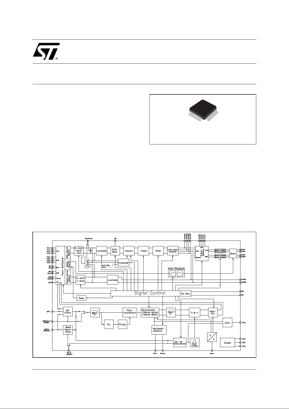
DESCRIPTION
The devic e includes a high performanc e audiopr ocessor
and a st ereodecoder-noiseblanker combination with the
whole low frequency signal processing necessary for
state-of-the-art as well as future carradios. The digital
control allows a programming in a wide range of all the
filter characteristics. Also the stereodecoder part offers
several possibilities of programming especially for the
adaptation to different IF -devices.
BLOCK DIAGRAM
October 2001
1/56
Page 2

TDA7405
SUPPLY
Symbol Parameter Test Condition Min. Typ. Max. Unit
V
Supply Voltage 7.5 9 10.5 V
s
I
Supply Current Vs = 9V 45 65 85 mA
s
SVRR Ripple Rejection @ 1KHz Audioprocessor(all Filters flat) 60 dB
Stereodecoder + Audioprocessor 55 dB
THERMAL DATA
Symbol Parameter Value Unit
R
Th j-pins
Thermal Resistance Junction-pins max 65 °C/W
ABSOLUTE MAXIMUM RATINGS
Symbol Parameter Value Unit
V
Operating Supply Voltage 10.5 V
s
T
T
Operating Temperature Range -40 to 85 °C
amb
Storage Temperature Range -55 to +150 °C
stg
ESD
All pins are protected against ESD according to the MIL883 standard.
PIN CONNECTION
(Top view
)
2/56
Page 3

TDA7405
BLOCK DIAGRAM
(Enlarged view)
3/56
Page 4

TDA7405
1 AUDIOPROCESSOR PART
Features:
Input Multiplexer 2 fully differential CD stereo inputs with programmable attenuation
1 single-ended stereo input
2 differential mono input
1 single-ended mono input
In-Gain 0..15dB, 1dB steps
internal Offset-cancellation (AutoZero)
separate second source-selector
Beep internal Beep with 3 frequencies + diagnostic setting (19kHz tone)
Mixing stage Beep, Phone,Navigation and FM mixable to all speaker-outputs (see Figure 20)
programmabe Voice-Band Filter
Loudness programmable center frequency and frequency response
15 x 1dB steps
selectable flat-mode (constant attenuation)
Volume 0.5dB attenuator
100dB range
soft-step control with programmable times
Bass 2nd order frequency response
center frequency programmable in 8 steps
DC gain programmable
± 15 x 1dB steps
Treble 2nd order frequency response
center frequency programmable in 4 steps
± 15 x 1dB steps
Equalizer two stereo equalizing-filters for separate front/rear adaption
1st filter center-frequency programmable i n 16 steps ( 4 steps/octav e, min 63Hz, max
840Hz)
2nd filter center-frequency programmable in 16 steps (4 steps/octave, min 300Hz,
max 4kHz)
quality factor programmable in 4 steps
± 15 x 1dB steps
selectable flat-mode
Speaker 4 independent speaker controls in 1dB steps
control range 95dB
separate Mute
Mute Functions direct mute
digitally controlled SoftMute with 4 programmable mute-times
Pause Detector programmable threshold
Compander dynamic range compression for use with CD
2:1 compression rate
programmable max. gain
4/56
Page 5
TDA7405
Table 1. ELECTRICAL CHARACTERISTICS
(VS=9V; T
Symbol Parameter Test Condition Min. Typ. Max. Unit
INPUT SELECTOR
R
in
V
CL
S
IN
G
IN MIN
G
IN MAX
G
STEP
V
DC
V
offset
DIFFERENTIAL STEREO INPUTS
R
in
G
CD
CMRR Common Mode Rejection Ratio V
e
NO
DIFFERENTIAL MONO INPUTS
R
in
CMRR Common Mode Rejection Ratio V
BEEP CONTROL
V
RMS
f
Beep
MIXING CONTROL
M
LEVEL
G
MAX
A
MAX
A
STEP
=25°C; RL=10kΩ; all gains=0dB; f=1kHz; unless otherwise specified)
amb
Input Resistance all single ended Inputs 70 100 130 kΩ
Clipping Level 2.2 2.6 V
Input Separation 80 100 dB
Min. Input Gain -1 0 +1 dB
Max. Input Gain 13 15 17 dB
Step Resolution 0.5 1 1.5 dB
DC Steps Adjacent Gain Steps -5 1 5 mV
G
MIN
to G
MAX
-10 1 10 mV
Remaining offset with AutoZero 0.5 mV
Input Resistance
Differential 70 100 130 kΩ
(see Fig. 1)
Gain only at true differential input -1 0 1 dB
-5 -6 -7 dB
-11 -12 -13 dB
= 1V
CM
= 1V
V
CM
@ 1kHz 46 70 dB
RMS
@ 10kHz 46 60 dB
RMS
Output-Noise @ Speaker-Outputs 20Hz - 20kHz, flat; all stages 0dB 9 15 µV
Input Impedance D ifferential 40 56 72 kΩ
= 1V
CM
= 1V
V
CM
Beep Level Mix-Gain = 6dB 250
Beep Frequency f
1. The Level for the 19kHz-Testtone is 2.1V
RMS
Beep1
f
Beep2
f
Beep3
f
Beep4
@ 1kHz 46 70 dB
RMS
@ 10kHz 46 60 dB
RMS
1)
350
500 mV
470 500 530 Hz
740 780 820 Hz
1.7 1.8 1 .9 kHz
18 19 2 0 kHz
Mixing Ratio Main / Mix-Source -6/-6 dB
Max. Gain 13 15 17 dB
Max. Attenuation -83 -79 -75 dB
Attennuation Step 0.5 1 1.5 dB
RMS
5/56
Page 6
TDA7405
Table 1. ELECTRICAL CHARACTERISTICS
(VS=9V; T
=25°C; RL=10kΩ; all gains=0dB; f=1kHz; unless otherwise specified)
amb
(continued)
Symbol Parameter Test Condition Min. Typ. Max. Unit
)
MULTIPLEXER OUTPUT
R
V
Output Impedance 800 1000 Ω
OUT
R
Output Load Capacitance 2 kΩ
L
C
L
DC Voltage Level 4.3 4.5 4.7 V
DC
2. If confgured as Multip le xer-Output
2
10 nF
LOUDNESS CONTROL
A
A
f
STEP
Peak
Step Resolution 0.5 1 1.5 dB
Max. Attenuation -21 -19 -17 dB
MAX
Peak Frequency f
P1
f
P2
f
P3
f
P4
180 200 220 Hz
360 400 440 Hz
540 600 660 Hz
720 800 880 Hz
VOLUME CONTROL
G
A
A
STEP
Max. Gain 30 32 34 dB
MAX
Max. Attenuation -83 -79.5 -75 dB
MAX
Step Resolution 0 0.5 1 dB
Attenuation Set Error G = -20 to +20dB -0.75 0 +0.75 dB
E
A
G = -80 to -20dB -4 0 3 dB
Tracking Error 2dB
E
T
V
DC Steps Adjacent Attenuation Steps 0.1 3 mV
DC
From 0dB to G
MIN
0.5 5 mV
SOFT MUTE
A
MUTE
Mute Attenuation 80 100 dB
Delay Time T1 0.48 1 ms
T
D
T2 0.96 2 ms
T3 70 123 170 ms
T4 200 324 600 ms
V
TH low
V
TH high
R
V
Low Threshold for SM-Pin
High Threshold for SM - Pin 2.5 V
Internal pull-up resistor 32 45 58 kΩ
PU
Internal pull-up Voltage 3.3 V
PU
3. The SM-Pin is active low (M ut e = 0)
3)
1V
BASS CONTROL
C
RANGE
A
STEP
Control Range ±14 +15.5 ±16 dB
Step Resolution 0.5 1 1.5 dB
6/56
Page 7

TDA7405
Table 1. ELECTRICAL CHARACTERISTICS
(VS=9V; T
=25°C; RL=10kΩ; all gains=0dB; f=1kHz; unless otherwise specified)
amb
(continued)
Symbol Parameter Test Condition Min. Typ. Max. Unit
f
Q
DC
C
BASS
GAIN
Center Frequency f
Quality Factor Q
C1
f
C2
f
C3
f
C4
f
C5
f
C6
f
C7
f
C8
1
Q
2
Q
3
Q
4
Bass-DC-Gain DC = off -1 0 +1 dB
54 60 66 Hz
63 70 77 Hz
72 80 88 Hz
81 90 99 Hz
90 100 110 Hz
117 130 143 Hz
135 150 165 Hz
180 200 220 Hz
0.9 1 1.1
1.1 1.25 1.4
1.3 1.5 1.7
1.8 2 2.2
DC = on 4 4.4 6 dB
TREBLE CONTROL
C
RANGE
A
STEP
PAUSE DETECTOR
V
Control Range ±14 +15 ±16 dB
Step Resolution 0.5 1 1.5 dB
Center Frequency f
f
C
4)
Zero Crossing Threshold Window 1 40 mV
TH
C1
f
C2
f
C3
f
C4
81012kHz
10 12.5 15 kHz
12 15 18 kHz
14 17.5 21 kHz
Window 2 80 mV
Window 3 160 mV
I
DELAY
V
Pull-Up Current 15 25 35 µA
Pause Threshold 3.0 V
THP
4. If configured as Pause-Output
SPEAKER ATTENUATORS
R
G
A
A
STEP
A
MUTE
V
Input Impedance 35 50 6 5 kΩ
in
Max. Gain 14 15 16 dB
MAX
Max. Attenuation -83 -79 -75 dB
MAX
Step Resolution 0.5 1 1.5 dB
Output Mute Attenuation 80 90 dB
Attenuation Set Error 2dB
E
E
DC Steps Adjacent Attenuation Steps 0.1 5 mV
DC
7/56
Page 8

TDA7405
Table 1. ELECTRICAL CHARACTERISTICS
(VS=9V; T
=25°C; RL=10kΩ; all gains=0dB; f=1kHz; unless otherwise specified)
amb
(continued)
Symbol Parameter Test Condition Min. Typ. Max. Unit
MONO VOICE BANDPASS
f
f
Highpass corner frequency f
HP
Lowpass corne r frequenc y f
LP
HP1
f
HP2
f
HP3
f
HP4
f
HP5
f
HP6
f
HP7
f
HP8
LP1
f
LP2
81 90 99 Hz
120 135 150 Hz
162 180 198 Hz
193 215 237 Hz
270 300 330 Hz
405 450 495 Hz
540 600 660 Hz
675 750 825 Hz
2.7 3 3.3 kHz
5.4 6 6.6 kHz
COMPANDER
G
max. Compander Gain Vi < -46dB 19 dB
MAX
Vi < -46dB, Anti-Clip=On 29 dB
t
t
V
C
Attack time t
Att
Release time t
Rel
Compander Reference Input-
REF
Level (equals 0dB)
Compression Factor Output Signal / Input Signal 0.5
F
Att1
t
Att2
t
Att3
t
Att4
Rel1
t
Rel2
t
Rel3
t
Rel4
V
REF1
V
REF2
V
REF3
6ms
12 ms
24 ms
49 ms
390 ms
780 ms
1.17 s
1.56 s
0.5 V
1.0 V
2.0 V
AUDIO OUTPUTS
V
R
V
Clipping Level d = 0.3% 2.2 2.6 V
CLIP
R
Output Load Resistance 2 kΩ
L
C
Output Load Capacitance 10 nF
L
Output Impedance 30 120 Ω
OUT
DC Voltage Level 4.3 4.5 4.7 V
DC
GENERAL
e
Output Noise BW = 20Hz - 20kHz;output muted 3 15 µV
NO
BW = 20Hz - 20kHz
all gains = 0dB
10 20 µV
single ended inputs
RMS
RMS
RMS
RMS
8/56
Page 9

TDA7405
Table 1. ELECTRICAL CHARACTERISTICS
(VS=9V; T
=25°C; RL=10kΩ; all gains=0dB; f=1kHz; unless otherwise specified)
amb
(continued)
Symbol Parameter Test Condition Min. Typ. Max. Unit
S/N Signal to Noise Ratio all gains = 0dB
= 2V
flat; V
O
RMS
bass, treble at +12dB;
a-weighted; V
d distortion V
S
Channel Separation left/right 80 100 dB
C
Total Tracking Error AV = 0 to -20dB -1 0 1 dB
E
T
= 1V
IN
V
= 1V
OUT
= -20 to -60dB -2 0 2 dB
A
V
; all stages 0dB 0.005 0.1 %
RMS
; Bass & Treble = 12dB
RMS
= 2.6V
O
RMS
106 dB
100 dB
0.05 0.1 %
9/56
Page 10

TDA7405
2 DESCRIPTION OF THE AUDIOPROCESSOR PART
2.1 Input stages
In the basic configuration two full-differential, tw o mono-differential, one single ended stereo and one singleended mono input are available. In addition a dedicated input for the stereodecoder MPX-signal is present.
Figure 1. Input stages
2.1.1 Full-differential stereo Input 1 (FD1)
The FD1-input is implemented as a buffered full-differential stereo stage with 100kΩ input-impedance at each
input. The attenuation is programmable in 3 steps from 0 to -12dB in order to adapt the incoming signal level.
A 6dB attenuation is included in the differ ential stage, the additi onal 6dB are done by a following r esi stive di vider. This input is also configurable as two single-ended stereo inputs (see pin-out).
2.1.2 Full-differential stereo Input 2 (FD2)
The FD2-input has the same general structure as FD1, but with a programmable attenuation of 0 or 6dB embedded in the differential stage.
10/56
Page 11

TDA7405
2.1.3 Mono-differential Input 1 (MD1)
The MD1-input is designed as a basic differential stage w ith 56kΩ input-impedance. This input is configurable
as a single-ended stereo input (see pin-out).
2.1.4 Mono-differential Input 2 (MD2)
The MD2-input has the same topology as MD1, but without the possibility to configure it to single ended.
2.1.5 Single-ended stereo Input (SE1), single-ended mono input (AM) and FM-MPX input
All single ended inputs offer an input impedance of 100kW. The AM-pin can be connected by software to the
input of the stereodecoder in order to use the AM-Noiseblanker and AM-High-Cut feature.
2.2 AutoZero
The AutoZero allows a reduction of the number of pins as wel l as external c omponents by c anceling any offset
generated by or before the In-Gain-stage (Please notice that externally generated offsets, e.g. generated
through the leakage current of the coupling capacitors, are not canceled).
The auto-zeroing is started every time the DATA-BYTE 0 is selected and needs max. 0.3ms for the alignment.
To avoid audible clicks the Audioprocessor is muted befor e the loudness stage during this time. The AutoZerofeature is only present in the main signal-path.
2.2.1 AutoZero for Stereodecoder-Selection
A special procedure is recommended for selecting the stereodecoder at the main input-selector to guarantee
an optimum offset-cancellation:
(Step 0: SoftMute or Mute the signal-path)
Step 1: Temporary deselect the stereodecoder at all input-selectors
Step 2: Configure the stereodecoder via IIC-Bus
Step 3: Wait 1ms
Step 4: Select the stereodecoder at the main input-selector first
The root cause of this procedure is, that after muting the stereodecoder (Step 1), the internal stereodecoder
filters have to settle in order to perform a proper offset-cancellation.
2.2.2 AutoZero-Remain
In some cases, for example if the µP is executing a refresh cycle of the IIC-Bus-programming, it is not useful
to start a new AutoZero-action because no new source is selected and an undesired mute would appear at the
outputs. For such applications the A631 could be switched in the AutoZero-Remain-Mode (Bit 6 of the subaddress-byte). If this bit is set to high, the DATABYTE 0 could be loaded without invoking the AutoZero and the
old adjustment-value remains.
2.3 Pause Detector / MUX-Output
The pin number 40(Pause/MUX) is configurable for two different functions:
1. During Pause-Detector OFF this pin is used as a mono-output of the main input-selector. This signal is
often used to drive a level-/equalizer-display on the carradio front-panel.
2. During Pause-Detector ON the pin is used to define the time-constant of the detector by an external capacitor.
The pause-detector is driven by the internal stereodecoder-outputs in order to use pauses in the FM-signal for
alternate-frequency-jumps. If the signal-level of both stereodecoder channels is outside the programmed voltage-window, the external capacitor is abruptly dis charged. Inside the pause-condition the capacitor is sl owly recharged by a constant current of 25µA. The pause information is also available via IIC-Bus (see IIC-Bus
programming).
11/56
Page 12

TDA7405
2.4 Loudness
There are four parameters programmable in the loudness stage:
2.4.1 Attenuation
Figure 2 shows the attenuation as a function of frequency at fP = 400Hz.
Figure 2. Loudness Attenuation @ fP = 400Hz
0.0
-5.0
-10.0
dB
-15.0
-20.0
-25.0
10.0 100.0 1.0K 10.0K
Hz
2.4.2 Peak Frequency
Figure 3 shows the four possible peak-frequencies at 200, 400, 600 and 800Hz
Figure 3. Loudness Center frequencies @ Attn. = 15dB
0.0
-5.0
dB
-10.0
12/56
-15.0
-20.0
10.0 100.0 1.0K 10.0K
Hz
Page 13

2.4.3 Loudness Order
Different shapes of 1st and 2nd-Order Loudness
Figure 4. 1st and 2nd Order Loudness @ Attn. = 15dB, fP=400Hz
TDA7405
0.0
-5.0
dB
-10.0
-15.0
-20.0
10.0 100.0 1.0K 10.0K
Hz
2.4.4 Flat Mode
In flat mode the loudness stage works as a 0dB to -19dB attenuator.
2.5 SoftMute
The digitally controlled SoftMute stage allows muting/demuting the signal with a I2C-bus programmable slope.
The mute process can either be activated by the SoftMute pin or by the I2C-bus. This slope is reali zed in a special S-shaped curve to mute slow in the critical regions (see Figure 5). For timing purposes the Bit of the I2Cbus output register is set to 1 from the start of muting until the end of de-muting.
Figure 5. Softmute-Timing
Note: Pleas e notice that a s tarted Mute -action is alway s terminated and could not be interrupt ed by a change of t he m ute -signal.
13/56
Page 14

TDA7405
2.6 SoftStep-Volume
When the volume-level is changed audible clicks could appear at the output. The root cause of those clicks
could either be a DC-Offset before the volume-stage or the sudden change of the envelope of the audiosignal.
With the SoftStep-feature both kinds of clicks could be reduced to a minimum and are no more audible. The
blend-time from one step to the next is programmable in four steps.
Figure 6. SoftStep-Timing
1dB
0.5dB
SS Time
-0.5dB
-1dB
Note: For steps more than 0.5dB the SoftStep mode should be deactivated because it could generate a hard 1dB step during the blend-time
2.7 Bass
There are four parameters programmable in the bass stage:
2.7.1 Attenuation
Figure 7 shows the attenuation as a function of frequency at a center frequency of 80Hz.
Figure 7. Bass Control @ fC = 80Hz, Q = 1
15.0
10.0
5.0
dB
0.0
-5.0
14/56
-10.0
-15.0
10.0 100.0 1.0K 10.0K
Hz
Page 15

2.7.2 Center Frequency
Figure 8 shows the eight possible center frequencies 60, 70, 80, 90, 100, 130, 150 and 200Hz.
Figure 8. Bass center Frequencies @ Gai n = 14dB, Q = 1
15.0
12.5
10.0
7.5
dB
5.0
2.5
0.0
TDA7405
10.0 100.0 1.0K 10.0K
Hz
2.7.3 Quality Factors
Figure 9 shows the four possible quality factors 1, 1.25, 1.5 and 2.
Figure 9. Bass Quality factors @ Gain = 14dB, fC = 80Hz
15.0
12.5
10.0
7.5
5.0
2.5
0.0
10.0 100.0 1.0K 10.0K
15/56
Page 16

TDA7405
2.7.4 DC Mode
In this mode the DC-gain is increased by 4.4dB. In addition the programmed center frequency and quality factor
is decreased by 25% which can be used to reach alternative center frequencies or quality factors.
Figure 10. Bass normal and DC Mode @ Gain = 14dB, fC = 80Hz
15.0
12.5
10.0
7.5
5.0
2.5
0.0
10.0 100.0 1.0K 10.0K
Note: The center frequency, Q and DC- m ode can be set full y independently.
2.8 Treble
There are two parameters programmable in the treble stage:
2.8.1 Attenuation
Figure 11 shows the attenuation as a function of frequency at a center frequency of 17.5kHz.
Figure 11. Tr ebl e C ontrol @ fC = 17.5kHz
15.0
10.0
5.0
0.0
-5.0
16/56
-10.0
-15.0
10.0 100.0 1.0K 10.0K
Page 17

2.8.2 Center Frequency
Figure 12 shows the four possible center frequencies 10k, 12.5k, 15k and 17.5kHz.
Figure 12. Treble Center Frequencies @ Gain = 14dB
15.0
12.5
10.0
7.5
5.0
2.5
0.0
TDA7405
10.0 100.0 1.0K 10.0K
2.9 EQ-Filter
There are two EQ-Filters present in the A631: one for the High-Frequency-Range and one for the Low-Fr equency-Range with a certain overlap. They ar e programmable in c enter -frequeny ( 4 frequencies /octave) , in Q(4 settings) and i n Attenuation (1dB-steps). In addition several configurations are possible to use the filters i n the fr ontor rear-path.
Table 2. Gain, Center Frequency and Quality Factor of Equalizer Filters
Parameter Min Max Unit
Gain -15 15 dB
Center Frequency Filter 1 63 840 Hz
Center Frequency Filter 2 300 4000 Hz
Quality Factor 1 4
17/56
Page 18

TDA7405
2.9.1 Equalizer-Setup
The two Filters can be configured in mul tiple ways in order to cov er as most as possible appl ications. Both filter s
can be programmed to be either in the front- or in the rear-path, respectively. This featur e enables to have e.g.
the High-Filter in the front- and both filters in the rear-path.
Figure 13. Equalizer Configuration
2.9.2 Attenuation
Figure 14 shows the attenuation as a function of frequency at a center frequency of 625 Hz.
Figure 14. Gain/Attenuation of EQ-Filter
15
dB
10
5
0
-5
-10
-15
2e+01
1e+02
1e+03
1e+04
Hz
2e+04
18/56
Page 19

2.9.3 Frequencies
Figure 15 shows the different center frequencies of the EQ-Filter at 12 dB gain
Figure 15. Cen te r- Frequencies of EQ - Fi lter
14
dB
12
10
8
6
4
2
0
TDA7405
-2
2e+01
1e+02
1e+03
2.9.4 Q-Factor
Figure 16 shows the four possible quality factors 1, 2, 3 and 4.
Figure 16. Different Q-factors of Equalizer-Filter
14
dB
12
10
8
6
4
2
0
1e+04
2e+04
Hz
-2
2e+01
1e+02
Hz
2e+04
1e+041e+03
19/56
Page 20

TDA7405
2.10Compander
2.10.1Signal-Compression
A fully integrated signal-compressor with programmable Attack- and Decay-times is present in the A631 (see
Figure 17). The compander consists of a signal-level detection, an A/D-Converter plus adder and the normal
SoftStep-Volume-stage. First of all t he left and the right InGai n-signal is recti fied, respec tively, and the logar ithm
is build from the summed signal. The following low-pass smooth the output-signal of the logarithm-amplifier and
improves the low-frequency suppression. The low-pass output-voltage then is A/D- converted an added to the
current volume-word defined by the IIC-Bus. Assuming reference-level or higher at the compander input, the
output of the ADC is 0. At lower levels the voltage is increasing with 1 Bit/dB. It is obvious that with this configuration and a 0.5dB-step volume-stage the compression rate is fixed to 2:1 (1dB less at the input leads to 0.5dB
less at the outpu t). The inter nal refer ence-level of the compander is p rogrammable in three steps from 0.5V
to 2V
the programmed reference-level after the InGain-stage. E.g. at a configured refer ence-level of 0.5V
put of the InGain-stage has to have also 0.5V
. For a proper behavior of the compr ess ion-circui t it is mandatory to hav e at a 0dB input-sign al exactl y
RMS
at 0dB source-signal (Usually the 0dB for CD is defined as
RMS
RMS
the maximum possible signal-lev el). To adapt the external level to the internal reference-level the programmable
attenuation in the differential-stages and the InGain can be used.
Figure 17. Compander Block Diagram
RMS
the out-
2.10.2Anti-Clipping
In a second ap pli cation the compander-circuit can be used for a Anti-Clipping or Limiting function. In this case one of
the dedicated inputs (AM or MPin) is connected directly to the Clip-Detector of the Power-Amplifier. If no clipping is
detected, the open-collector output of the Power-Amplifier is highohmic and the input-voltage of the rectifier is V
REF
The level-detector interprets this as a very small signal and react s with the maximum programmed compander-gain.
In the application this gain has to be compensated by decreasing the volume wit h the same value in order to get the
desired output-level. In clipping situation the open-collect or-current generates a voltage-drop at the rectifier-input,
which forces the compander to decrease the gain until the clipping disappears .
It is even possible to run the compression-mode and the Anti-Clipping mode in par allel. In this case the maximum compander-Gain should be set to 29 dB.
20/56
.
Page 21

TDA7405
2.10.3Characteristic
To achieve the desired compression characteristic like shown below the volume has to be decreased by 4dB.
Figure 18. Compander Characteristic
0
-10
Output Level
-20
dB
-30
-40
-50
-60
0
-8dB
2:1
-38dB
15dB
-10 -20 -30 -40 -50 -60
Input Level
dB
2.10 .4I² C -BUS-Timing
When the Compander is active a volume- word coming from this stage is added to the I2C-Bus volume-w ord
and the volume is changed with a soft slope between adjacent steps (SoftStep-stage). As mentioned in the description of this stage it is not recommended to change the volume during this slope. To avoid this behaviourwhile the Compander is working, and the volume has to be changed, the compander-hold-bit is implemented
(Bit 7 in the subaddress-byte). The recommended timing for changing the volume during compander-ON is the
following:
1. Set the compander-hold-bit
2. Wait the actual SoftStep-time
3. Change the volume
4. Reset the compander-hold-bit
The SoftStep-times are in compander- ON condition automatically adapted to the attac k-time of the Compander.
In the following table the related SoftStep-times are shown:
Attack-Time SoftStep-Time
6ms 0.16ms
12ms 0.32ms
24ms 0.64ms
48ms 1.28ms
2.10.5AC-Coupling
In some applications additional signal manipulations are desired, for example surround-sound or more-bandequalizing. For this purpose an AC-Coupling is placed before the speaker-attenuators, w hich can be activated
or internally shorted by I²C-Bus. In short condition the input-signal of the speaker-attenuator is available at the
AC-Outputs. The input-impedance of this AC-Inputs is 50k
Ω
.
21/56
Page 22

TDA7405
2.10 .6O utput Selec tor
The output-selector allows to connect the main- or the second-source to the Front-, Rear-speaker-attenuator,
respectively. As an example of this programming the device is able to connect via software the main-source to
the back (rear) and the second-source to the front (see Figure 19).
Figure 19. Output Selector
2.10.7S peake r-Attenu ator and Mixing
A Mixing-stage is placed after each speaker-attenuator and can be set independently to mixing-mode. Having
a full volume for the Mix-signal the stage offers a wide flexibility to adapt the mixing levels.
Figure 20. Mixing Configuration
2.10.8Aud iopro cesso r Testi ng
During the Testmode, which can be activated by setting bit D0 of the stereodecoder testing-byte and the audioprocessor testing byte, several internal signals are available at the FD2R- pin. During this mode the input resistance of 100kOhm is disconnected from the pin. The internal signals available are shown in the Data-byte
specification.
22/56
Page 23

TDA7405
3 STEREODECODER-PART
3.1 Features:
■
no external components necessary
■
PLL with adjustment free, fully integrated VCO
■
automatic pilot dependent MONO/STEREO switching
■
very high suppression of intermodulation and interference
■
programmable Roll-Off compensation
■
dedicated RDS-Softmute
■
Highcut- and Stereoblend-characterisctics programmable in a wide range
■
FM/AMNoiseblanker with several threshold controls
■
Multipath-detector with programmable internal/external influence
■
I2C-bus control of all necessary functions
Table 3. ELECTRICAL CHARACTERISTICS
V
= 9V, deemphasis time constant = 50µs, MPX input voltage V
S
modulation frequency = 1kHz, input gain = 6dB, T
= 27°C, unless otherwise specified.
amb
Symbol Parameter Test Conditions Min. Typ. Max. Unit
= 500mV (75kHz deviation),
MPX
V
MPX Input Level Input Gain = 3.5dB 0.5 1.25 V
in
R
G
G
G
SVRR Supply Voltage Ripple Rejection V
Input Resistance 70 100 130 kΩ
in
Min. Input Gain 1.5 3.5 4.5 dB
min
Max. Input Gain 8.5 11 1 2.5 dB
max
Step Resolution 1.75 2.5 3.25 d B
step
= 100mV, f = 1kHz 55 dB
ripple
α Max. Chan nel Separatio n 30 50 d B
THD Total Harmonic Distortion f
SN+
--------------
Signal plus Noise to Noise Ratio A-weighted, S = 2V
N
=1kHz, mono 0.02 0.3 %
in
rms
80 91 dB
MONO/STEREO-SWITCH
V
PTHST1
V
PTHST0
V
PTHMO1
V
PTHMO0
Pilot Threshold Voltage for Stereo, PTH = 1 10 15 25 mV
Pilot Threshold Voltage for Stereo, PTH = 0 15 25 35 mV
Pilot Threshold Voltage for Mono, PTH = 1 7 12 17 mV
Pilot Threshold Voltage for Mono, PTH = 0 10 19 25 mV
PLL
rms
∆f/f Capture Range 0.5 %
23/56
Page 24

TDA7405
Table 3. ELECTRICAL CHARACTERISTICS
V
= 9V, deemphasis time constant = 50µs, MPX input voltage V
S
modulation frequency = 1kHz, input gain = 6dB, T
(continued)
= 27°C, unless otherwise specified.
amb
= 500mV (75kHz deviation),
MPX
Symbol Parameter Test Conditions Min. Typ. Max. Unit
DEEMPHASIS and HIGHCUT
τ
DeempF
M
M
FM
τ
DeempA
M
M
AM
Deemphasis Timeconstants FM V
Highcut Timeconst ant Multiplier FM
Deemphasis Timeconstants AM V
Highcut Timeconstant Multiplier AMV
LEVEL
V
LEVEL
V
LEVEL
V
LEVEL
V
LEVEL
LEVEL
V
LEVEL
V
LEVEL
V
LEVEL
LEVEL
>> V
>> V
>> V
>> V
<< V
>> V
>> V
>> V
>> V
<< V
HCH
HCH
HCH
HCH
HCL
HCH
HCH
HCH
HCH
HCL
25 50 75 µs
44 62.5 80 µs
50 75 100 µs
70 100 130 µs
3
37.5 µs
47 µs
56 µs
75 µs
3.7
REF5V Internal Reference Voltage 4.7 5 5.3 V
L
L
maxs
L
Gstep
VSBL
VSBL
VSBL
VHCH
VHCH
VHCH
VHCL
VHCL
VHCL
min. LEVEL Gain -1 0 1 dB
min
max. LEVEL Gain 5 6 7 dB
LEVEL Gain Step Resolution see section 2.7 0.2 0.4 0.6 dB
Min. Voltage for Mono see section 2.8 17 20 23 %REF5V
min
Max. Voltage for Mono see section 2.8 62 70 78 %REF5V
max
Step Resolution see section 2.8 1.6 3.3 5.0 %REF5V
step
Min. Voltage for NO Highcut see section 2.9 37 42 47 %REF5V
min
Max. Voltage for NO Highcut see section 2.9 58 66 74 %REF5V
max
Step Resolution see section 2.9 4.2 8.4 12.6 %REF5V
step
Min. Voltage for FULL High cut see section 2.9 15 17 19 %VHCH
min
Max. Voltage for FULL High cut see section 2.9 29 33 37 %VHCH
max
Step Resolution see section 2.9 2.1 4.2 6.3 %REF5V
step
Carrier and harmonic suppression at the output
α19 Pilot Signalf=19 kHz 40 50 d B
α38 Subcarrier f=38kHz 75 dB
α57 Subcarrier f=57kHz 62 dB
α76 Subcarrier f=76kHz 90 dB
24/56
Page 25

TDA7405
Table 3. ELECTRICAL CHARACTERISTICS
V
= 9V, deemphasis time constant = 50µs, MPX input voltage V
S
modulation frequency = 1kHz, input gain = 6dB, T
Symbol Parameter Test Conditions Min. Typ. Max. Unit
Intermodulation (Note 1)
α2f
α3f
Traffic Radio (Note 2)
α57 Signal f=57kHz 70 dB
SCA - Subsidiary Communications Authorization (Note 3)
α67 Signal f=67kHz 75 dB
ACI - Adjacent Channel Interference (Note 4)
α114 Signal f=114kHz 95 dB
α190 Signal f=190kHz 84 dB
=10kHz, f
mod
=13kHz, f
mod
=1kHz 65 dB
spur
=1kHz 75 dB
spur
(continued)
= 27°C, unless otherwise specified.
amb
= 500mV (75kHz deviation),
MPX
Notes to the Characteristics
Note 1.
Intermodulation Suppression
V
o
--------------------------------------------------------------- -
α
2
()
spurious
V
o
()
signal
()
at1kHz
()
at1kHz
;
ƒ
s
⋅()
210kHz
–==
19kH z
3
()
spurious
V
o
()
signal
V
o
--------------------------------------------------------------- -
α
()
at1kHz
()
at1kHz
;
ƒ
s
⋅()
313kHz
–==
38kH z
measured with: 91% pilot signal; fm = 10 kHz or 13 kHz.
Note 2.
Traffic Radio (V.F.) Suppression
measured with: 91% stereo signal; 9% pilot signal; fm=1kHz; 5% subcarrier (f=57kHz, fm=23Hz AM, m=60%)
Note 3.
()
V
signal
α
()
57 V.W.F.
------------------------------------------------------------------------------------ -=
V
o
()
spurious
o
SCA ( Subsidiary Communications Authorization )
()
signal
V
o
α
--------------------------------------------------------------- -
67
()
spurious
V
o
()
at1kHz
()
at9kHz
()
at1kHz
()
at1kHz±23kHz
;
ƒ
s
⋅()
338kHz
–==
67kHz
measured with: 81% mono signal; 9% pi lot sig nal; fm=1kH z; 10%SCA - subc ar rier ( fs = 67kHz, unmod ulated ) .
25/56
Page 26

TDA7405
Note 4.
ACI ( Adjacent Channel Interference )
()
signal
V
o
α
114
α
190
--------------------------------------------------------------- -
()
spurious
V
o
()
signal
V
o
--------------------------------------------------------------- -
()
spurious
V
o
()
at1kHz
()
at4kHz
()
at1kHz
()
at4kHz
;
ƒ
s
;
ƒ
s
110 kHz 3 38kHz
186 kHz 5 38kHz
⋅()–==
⋅()–==
measured with: 90% mono signal; 9% pilot signal; fm=1kHz; 1% spurious signal (f
modulated).
NOISE BLANKER PART
Features:
■
AM and FM mode
■
internal 2nd order 140kHz high-pass filter for MPX path
■
internal rectifier and filters for AM-IF path
■
programmable trigger thresholds
■
trigger threshold dependent on high frequency noise with programmable gain
■
additional circuits for deviation- and fieldstrength-dependent trigger adjustment
■
4 selectable pulse suppression times for each mode
■
programmable noise rectifier charge/discharge current
= 110kHz or 186kHz, un-
s
Table 4. ELECTRICAL CHARACTERISTICS
All parameters mesured in FM mode if not otherwise specified.
Symbol Parameter Test conditions Min. Typ. Max. Unit
V
V
TRNOISE
TR
Trigger Thres hold
noise controlled
Trigger Thres hold
5)
meas.with
=0.9V
V
PEAK
meas.with
=1.5V
V
PEAK
111 30 mV
110 35 mV
101 40 mV
100 45 mV
011 50 mV
010 55 mV
001 60 mV
000 65 mV
00 260 mV
01 220 mV
10 180 mV
11 140 mV
OP
OP
OP
OP
OP
OP
OP
OP
OP
OP
OP
OP
26/56
Page 27

TDA7405
Table 4. ELECTRICAL CHARACTERISTICS
(continued)
All parameters mesured in FM mode if not otherwise specified.
Symbol Parameter Test conditions Min. Typ. Max. Unit
V
V
V
RECT
RECT
T
T
Rectifier Voltage V
RECT
Deviation dependent
DEV
Rectifier Voltage
Fieldstrength
FS
controlled Rectifier
Voltage
Suppression Pulse Duration FM Signal HOLDN
SFM
Suppression Pulse Duration AM Signal HOLDN
SAM
=0mV 0.5 0.9 1.3 V
MPX
V
=50mV, f=150kHz 1.5 1.7 2.1 V
MPX
V
=200mV, f=150kHz 2 2.5 2.9 V
MPX
meas.with
=500mV
V
MPX
(75kHz dev.)
meas.with
=0mV,
V
MPX
V
<< V
LEVEL
(fully mono)
in Testmode
in Testmode
SBL
11
10
01
00
11
10
01
00
00
01
10
11
00
01
10
11
0.5
0.9
1.7
2.5
0.5
0.9
1.7
2.1
0.9 (off)
1.2
2.0
2.8
0.9 (off)
1.4
1.9
2.4
38
25.5
32
22
1.2
800
1.0
640
1.3
1.5
2.3
3.1
1.3
1.5
2.3
3.1
V
V
V
V
OP
OP
OP
OP
V
V
V
V
µs
µs
µs
µs
ms
µs
ms
µs
V
RECTADJ
SR
V
ADJMP
R
G
AMIF,min
Noise rectifier discharge
adjustment
Noise rectifier
PEAK
charge
Noise rectifier adjustment
through
Multipath
AM IF Input resistance 35 50 65 kOhm
AMIF
min. gain AM IF Signal AM-RECTIFIER in
Signal PEAK in
Testmode
Signal PEAK in
Testmode
Signal PEAK in
Testmode
00
01
10
11
0
1
00
01
10
11
0.3
0.8
1.3
2.0
10
20
0.3
0.5
0.7
0.9
6dB
Testmode
G
G
f
AMIF,max
AMIF,step
AMIF,min
max. gain AM IF 20 dB
step gain AM IF 2 dB
min. fc AM IF Signal AM-RECTIFIER in
14 kHz
Testmode
f
AMIF,max
max. fc AM IF 56 kHz
5.All thresholds are measured using a pulse with TR = 2 µs, THIGH= 2 µs and TF = 10 µ s. The repe ti ti on rate mu st not increa se the PE AK voltage.
V/ms
mV/µs
V/ms
27/56
Page 28

TDA7405
Figure 21. Noiseblanker Test-Pulse
V
in
DC
V
op
T
R
Figure 2 2. Trigger Threshold vs. VPEAK
VTH
MIN. TRIG. THRESHOLD NOISE CONTROLLED TRIG . THRESHOLD
T
HIGH
T
F
Time
260mV (00)
220mV (01)
180mV (10)
140mV (11)
28/56
8 STEPS
65mV
30mV
1.5V0.9V
V
PEAK [V]
Page 29

Figure 23.
V
PEAK
[V ]
OP
2. 8
2. 0
1. 2
0.9
TDA7405
00
01
10
D ete cto r off ( 1 1)
20
32.5 45 75
Figure 24. Fiel dst renth Control l ed Tri gger Adjustment
V
PEAK
MONO STEREO
≈
3V
NOISE
ATC_SB OF F (11)
noisy signal
2.4V (00)
1.9V (01)
1.4V (10)
good signal
DEVIATION [KHz ]
0.9V
E'
29/56
Page 30

TDA7405
MULTIPATH DETECTOR
Features:
■
internal 19kHz band-pass filter
■
programmable band-pass- and rectifier-gain
■
selectable internal influence on Stereoblend and/or Highcut
Table 5. ELECTRICAL CHARACTERISTICS
Symbol Parameter Test Conditions Min. Typ. Max. Unit
f
CMP
Center frequency of MultipathBandpass
G
BPMP
G
RECTMP
I
CHMP
I
DISMP
Bandpass Gain G1 6 dB
Rectifier Gain G1 7.6 dB
Rectifier Charge Current 0.25
Rectifier Discharge Current 4 mA
Quality Detector
A
Multipath
Influence Factor
stereodecoder locked on Pilottone 19 kHz
G2 12 dB
G3 16 dB
G4 18 dB
G2 4.6 dB
G3 0 dB
0.5
00
01
10
11
0.70
0.85
1.00
1.15
µA
4 FUNCTIONAL DESCRIPTION OF STEREODECODER
Figure 25. Blockdiagram of the Stereodecoder
30/56
Page 31

TDA7405
The stereodecoder-part of the A631 (see Figure 25) contains all functions necessary to demodulate the MPXsignal like pilottone-dependent MONO/STEREO-switching as well as "stereoblend" and "highcut". Adaptations
like programmable input gain, rol l-off compensation, selectable deemphasis time constant and a programmable
fieldstrength input allow to use different IF-devices.
4.1 Stereodecoder-Mute
The A631 has a fas t and easy to contr ol RDS-Mute function which is a combination of the audi oprocessor's SoftMute and the high-ohmic mute of the s t ereodecoder. If the stereodecoder is selec ted and a SoftMute command
is sent (or activ ated through the SM-pin) the stereod ecoder will be set automatical ly to the high-ohmi c mute condition after the audio-si gnal has been softmuted. Hence a checking of alternate frequenc ies could be performed.
Additionally the PLL can be set to "Hold"-mode, which disables the PLL input during the mute time. To release
the system from the mute condition simply the unmute-command must be sent: the stereodecoder is unmuted
immediately and the audioprocessor is softly unmuted. Figure 26 shows the output-signal VO as well as the internal stereodecoder mute sign al. This influence of S oftMute on th e stereodecoder mute can b e switched off by
setting bit 3 of the SoftMute byte to "0". A stereodecoder mute command (bit 0, stereodecoder byte set to "1")
will set the stereodecoder in any case independently to the high-ohmic mute state.
If any other source than the stereodecoder is selected the decoder r emains muted and th e MPX-pin is c onnected to V
should be applied.
Figure 26. Signals during stereodecoder's SoftMute
to avoid any discharge of the coupl ing capac itor through leakage c ur rents. No further mute c ommand
ref
Figure 27. Signal-Control via SoftMute-Pin
31/56
Page 32

TDA7405
4.2 InGain + Infilter
The InGain stage allows to adjust the MPX-signal to a magnitude of about 1Vrms internally which is the recommended value. The 4.th order input filter has a corner frequency of 80kHz and is used to attenuate spikes and
noise and acts as an anti-aliasing filter for the following switch capacitor filters.
4.3 Demodulator
In the demodulator block the left and the right channel are separated from the MPX-signal. In this stage also the
19-kHz pilottone is c ancelled. For reaching a high channel separ ation the A631 offer s an I
roll-off adjustment which is able to compensate the lowpass behavior of the tuner section. If the tuner's attenuation at 38kHz is in a range from 7.2% to 31.0% the A631 needs no external network in front of the MPX-pin.
Within this range an adjustment to obtain at least 40 dB channel separation is possible. The bits for this adjustment are located together wi th the fieldstrength adjustment in one byte. This gives the possibility to perform an
optimization step during the production of the carradio where the channel separation and the fieldstrength control are trimmed. The setup of the Stereoblend characteristics which is programmable in a wide range is described in 2.8.
4.4 Deemphasis and Highcut
.The deemphasis-lowpass all ows to cho ose a time co nstant between 37.5 and 100µs. The high cut control range
will be 2 x t
Deemp
or 2.7 x t
dependent on the selected time constant (see programming section). The bit
Deemp
D7 of the hightcut-byte will shift timeconstant and range.
Inside the highcut control range (between VHCH and VHCL) the LEVEL signal is converted into a 5 bit word
which controls the lowpass time constant between t
Deem p.. .3
(3.7) x t
. Thereby the resolution will remain
Deemp
always 5 bits independently of the absolute voltage range between the VHCH- and VHCL-values. In addition
the maximum attenuation can be fixed between 2 and 10dB.
2
The highcut function can be switched off by I
C-bus (bit D7, Highcut byte set to "0").
The setup of the highcut characteristics is described in 4.9.
2
C-bus programmable
4.5 PLL and Pilottone-Detector
The PLL has the task to lock on the 19kHz pilottone during a stereo-transmission to allow a correct demodulation. The included pilottone-detector enables the demodulation if the pilottone reaches the selected pilottone
threshold VPTHST. Two different thresholds are available. The detector output (signal STEREO, see Blockdiagram) can be checked by reading the status byte of the A631 via I
2
C-bus. During a Softmute the PLL can be
set into "Hold"-mode which freezes the PLL's state (bit D4, Softmute byte). After releasing the Softmute the PLL
will again follow the input signal only by correcting the phase error.
4.6 Fieldstrength Control
The fieldstrength input is used to control the highcut- and the stereoblend-function. In addition the signal can be
also used to control the noiseblanker thresholds and as input for the multipath detector. These additional functions are described in sections 3.3 and 4.
4.7 LEVEL-Input and -Gain
To suppress undesired high frequency modulation on the highcut- and ster eoblend-control signal the LEVEL
signal is lowpass filtered firs tly. The filter is a combination of a 1.st-order RC-lowpass at 53kHz (working as antialiasing filter) and a 1.st-order switched -capacitor-low pass at 2.2k Hz. The second s tage is a programmable gain
stage to adapt the LEVEL signal internally to different IF-devices (see Testmode section 5: LEVELHCC). The
gain is widely programmable in 16 steps from 0dB to 6dB (step=0.4dB). These 4 bits are located together wi th
the Roll-Off bits i n the "Stereodec oder-Adjus tment"-byte to si mplify a possible adjustment during the produc tion
of the carradio. This signal controls directly the Highcut stage whereas the signal is filtered again (fc=100Hz)
before the stereoblend stage (see Figure 25).
32/56
Page 33

TDA7405
4.8 Stereoblend Control
The stereoblend control bloc k con ver ts the internal LEV EL-volt age (LEVELSB) i nto an demodu lator compati ble
analog signal which is used to control the channel separation betwe en 0dB and the maxi mum separation. Internally this control range has a fixed upper limit which is the inter nal reference voltage REF5V. The lower limit can
be programmed between 20 and 70% of REF5V in 3.3% steps (see Figure 28, Figure 29).
To adjust the external LEVEL-voltage to the internal range two values must be defined: the LEVEL gain LG and
VSBL (see Figure 29). At the point of full channel separation the external level signal has to be amplified that
internally it be comes equal to REF5V. The s econd point (e.g. 10dB channel sep.) is then adjusted w ith the VSBL
voltage.
Figure 28. Internal stereoblend characteristics
The gain can be programmed through 4 bits in the "Stereodecoder-Adjustment"-byte. All necessary internal reference voltages like REF5V are derived from a bandgap circuit. Therefore they have a temperature coefficient
near zero.
Figure 29. Relation between internal and external LEVEL-voltages for setup of Stereoblend
70
20
4.9 Highcut Control
The highcut control setup is similar to the stereoblend control setup : the starting point VHCH can be set with 2
bits to be 42, 50, 58 or 66% of R EF5V whereas the range can be set to be 17, 22, 28 or 33% of VHCH (see
Figure 30).
33/56
Page 34

TDA7405
Figure 30. Highcut characteristics
5 FUNCTIONAL DESCRIPTION OF THE NOISEBLANKER
In the automotive environment the MPX-signal as well as the AM-signal is disturbed by spikes produced by the
ignition and other radiating sources li ke the wiper-motor. The aim of the noiseblanker part is to cancel the audible influence of the spikes. Therefore the output of the stereodecoder is held at the actual voltage for a time
between 22 and 38µs in FM (370 and 645µs in AM-mode). The blockdiagram of the noiseblanker is given in
Figure 31.
Figure 31. Block diagram of the noiseblanker
In a first stage the spikes must be detected but to avoid a wrong triggering on high frequency (white) noise a
complex trigger control is implemen ted. Behind the triggerstage a pulse former generates the "blanking "-pulse.
5.1 Trigger Path FM
The incoming MPX signal is highpass-filtered, amplified and rectified. This second order highpass-filter has a
corner-frequency of 140kHz. The rectified signal, RECT, is integrated (lowpass filtered) to generate a signal
called PEAK. The DC-charge/discharge behaviour can be adjusted as well as the transient behaviour(MP-discharge control). Also noise with a frequency 140kHz increases the PEAK voltage. The PEAK voltage is fed to
a threshold generator, which adds to the PEAK-voltage a DC-dependent threshold VTH. Both signals, RECT
and PEAK+VTH are fed to a comparator which triggers a re-triggerable monoflop. The monoflop's output activates the sample-and-hold circuits in the signalpath for the selected duration
5.2 Noise Co ntrolled Threshold Adjus tment (NCT)
There are mainly two independent possibilities for programming the trigger threshold:
1. the low threshold in 8 steps (bits D
2. and the noise adjusted thr eshold in 4 steps (bits D
34/56
to D3 of the noiseblanker-byte I)
1
and D5 of the noiseblanker-byte I, see Figure 22).
4
Page 35

TDA7405
The low threshold is active in combinati on with a good MPX signal w ithout nois e; the PEAK voltage is les s than
1V. The sensitivity in this operation is high. If the MPX signal is noisy (low fieldstrength) the PEAK voltage increases due to the higher noise, which is als o recti fied. With inc reasing of the PEAK volta ge the trigger thr eshold
increases, too. This gain is programmable in 4 steps (see Figure 22).
5.3 Additional Threshold Control Mechanism
5.3.1 Automatic Threshold Control by the Stereob lend vo ltage
Besides the noise controlled threshold adjustment there is an additional possibility for influencing the trigger
threshold which depends on the stereoblend control.
The point where the MPX signal star ts to become nois y is fixed by the RF part. Ther efore als o the starting point
of the normal noise-controlled trigger adjustment is fixed (Figure 24). In some cases the behavior of the noiseblanker can be improved by increasing the threshold even in a region of higher fieldstrength. Sometimes a
wrong triggering occurs for the MPX signal often shows distortion in this range which can be avoided even if
using a low threshold. Because of the overlap of this range and the range of the stereo/mono transition it can
be controlled by stereoblend. This increase of the threshold is programmable in 3 steps or switched off.
5.3.2 Over Deviation Detector
If the system is tuned to stations with a high deviation the noiseblanker can trigger on the higher frequencies
of the modulation or distortion. To avoid this behavior, which causes audible noise in the output signal, the
noiseblanker offers a deviation-dependent threshold adjustment. By rectifying the MPX signal a further signal
representing the actual deviation is obtained. It is used to increase the PEAK voltage. Offset and gain of this
circuit are programmab le in 3 s teps with the bi ts D
off the detector, see Figure 23).
and D7 of the noiseblanker-byte I ( bit c ombination '00' turns
6
5.3.3 Multipath-Level
To react on high repetitive spikes caused by a Multipath-situation, the discharge-time of the PE AK voltage can
be decreased depending on the vol t age-level at pin M Pout. The A63 1 offers a linear as wel l as a threshold driven control. The linear influence of the Multipath-Level on the PEAK-signal (D
a discharge slewrate of 1V/ms
switches on the 18kOhm discharge if the Multipath-Level is below 2.5V (D
1
The slewrate is measured with R
1
. The second possibility is to activate the threshold driven discharge which
Discharge
= nfinite and V
MPout
= 2.5V
of Multipath-Control-Byte) gives
7
of noiseblanker-byte II-byte).
7
5.3.4 AM mode of the Noiseblanker
The A631 noiseblanker is also suitable for AM noise canceling. The detector uses in AM mode the 450kHz unfiltered IF-output of the tuner for spike detection. A combination of programmable gain-stage and lowpass-filter
forms an envelope detector which drives the noiseblanker's input via a 120 kHz 1.st order highpass. In order to
blank the whole spike in AM mode the hold-times of the sample and hold circuit are much longer then in FM
(640µs to 1.2ms). All threshold controls can be used like in FM mode.
5.4 Functional Description of the Multipath-Detector
Using the Multipath-Detector the audible effects of a multipath condition can be minimized. A multipath-condition is detected by rectifyi ng the spectr um around 19kH z in the fieldstrength si gnal. An exter nal capacitor is used
to define the attack- and decay-times for the Stereoblend (see blockdiagram, Figure 32). Due to the very small
charge currents this capacitor should be a low leakage current type (e.g. ceramic). U sing this configuration an
adaptation to the user's requirement is possible w ithout effecting the "normal" fieldstrength input (LEVEL) for
the stereodecoder. This application is given in Figure 32. Another (internal) time constant is used to c ontro l the
Highcut through the multipath detector
Selecting the "internal influence" in the configuration byte the Stereo-Blend and/or the Highcut is automatically
invoked during a multipath condition according to the voltage appearing at the MP_OUT-pin.
35/56
Page 36

TDA7405
Figure 32. Bl ock d iagram of the M ul tipath-Detect or
5.5 Quality Detector
The TDA7405 offers a quality detector output which gives a voltage representing the FM-reception conditions.
To calculate this voltage the MPX-noise and the multipath- detec tor output are summed according to the following formula :
V
Qual
= 1.6 (V
-0.8 V)+ a (REF5V-V
Noise
Mpout
).
The noise-signal is the PEAK-signal without additional influences (see noiseblanker description). The factor 'a'
can by programmed to 0.7 .... 1.15. The output is a low impedance output able to drive ex ternal circui try as well
as simply fed to an AD-converter for RDS applications.
36/56
Page 37

TDA7405
5.6 Dual-MPX Mode
The TDA7405 is able to support a twin tuner con cept v ia the Dual-MPX-Mode. In thi s configuration the MPX-pin
and the MD2G-pin ar e acti ng as MPX1 and MPX2 inputs . The D C-Voltage at the MD2-pin contr ols whether one
or both MPX-signals are used to decode the stereo FM-signal. It is designed as a window-comparator with the
characteristic shown in Figure 33 (Please note that the thresholds have a hysteresis of 500mV). In this mode
the stereodecoder highohmic-mute mutes both inputs in parallel.
Figure 33. Blockdiagram Dual MPX
Table 6. Pin-Configuration DMPX-/WSM-Mode
Dual MPX
off off AMIF-In not used not used MD2-In MD2-Gnd
off on WSM-TC WSM-In WSM-Out MD2-In MD2-Gnd
on off AMIF-In DMPC-Cntrl MPX2 MD2-In MD2-Gnd
on on WSM-TC WSM-In WSM-Out DMPC-Cntrl MPX2
Weak-Signal
Mute
AMIF(12) DMPXC(25) MPX2(26) MD2(43) MD2G(44)
5.7 Weak-Signal Mute
For use with front-ends which do not support a weak-signal-mute function the TDA7405 offers this feature as
well. If this mode is enabled the pins 26 and 27 are used as an AC-coupling behind the Mute-Stage (see blockdiagram). In parallel pin 12 (AMIF) is switched internally to realize a mute time-constant with fast attack - and
slow decay-time.
37/56
Page 38

TDA7405
Figure 34. Weak-Signal Mute-Depth @ 0.5V Threshold
5
0
-5
-10
-15
-20
Mute Depth / dB
-25
-30
-35
-40
0.0 0.80.1 0.70.2 0.60.3 0.50.4
Level Voltage / V
Figure 35. Weak-Signal Mute-Threshold @ 24dB Mute-Depth
5
0
-5
-10
-15
Mute Depth / dB
-20
-25
-30
0.0
0.1 0.70.2 0.60.3 0.50.4
Level Voltage / V
0.8
5.8 Stereodecoder Testmode
During the Testmode, which can be activated by setting bit D0 and bit D1 of the stereodecoder testing-byte,
several internal signals are available at the FD2R+ pin. During this mode the input resistance of 100kOhm is
disconnected from the pin. The internal signals available are shown in the Data-byte specification.
38/56
Page 39

6 I²C BUS INTERFACE
6.1 Interface Protocol
The interface protocol comprises:
-a start condition (S)
-a chip address byte (the LSB bit determines read / write transmission)
-a subaddress byte
-a sequence of data (N-bytes + acknowledge)
-a stop condition (P)
CHIP ADDRESS SUBADDRESS DATA 1 ... DATA n
TDA7405
MSB
S1000110R/WACKCAZIAAAAAACK DATA ACK P
LSB MSB LSB MSB LSB
S = Start
R/W ="0" -> Receive-Mode (Chip could be programmed by µP)
"1" -> Transmission-Mode (Data could be received by µP)
ACK = Acknowledge
P = Stop
MAX CLOCK SPEED 500kbits/s
6.1.1 Auto increment
If bit I in the subaddress byte is set to "1", the autoincrement of the subaddress is enabled.
6.1.2 TRANSMITTED DATA (send mode)
MSB LSB
ST
XXXXXP
SM
SM = Soft mute activated
ST = Stereo
P = Pause
X = Not Used
The transmitted data is automatically updated after each ACK. Transmission can be repeated without new chi-
paddress.
6.1.3 Reset Condition
A Power-On-Reset is invoked if the Supply-Voltage is below than 3.5V. After that the following data is written
automatically into the registers of all subaddresses :
MSB LSB
1
111111
0
The programming after POR is marked bold-face / under lined in the programming tables.
With this programming all the outputs are muted to V
REF
(V
OUT
= VDD/2).
39/56
Page 40

TDA7405
6.2 SUBADDRESS (receive mode)
MSB
I
I
2
I
1
A
0
A
4
3
LSB
FUNCTION
A
A
2
A
1
0
0
1
off
on
AutoZero Remain
Compander Hold
0
1
off
on
Auto-Increment Mode
0
1
off
on
Subaddress
0
0
0
0
0
0
0
0
0
0
0
0
0
0
0
0
1
1
1
1
1
1
1
1
1
1
1
1
1
1
1
1
0
0
0
0
0
0
0
0
1
1
1
1
1
1
1
1
0
0
0
0
0
0
0
0
1
1
1
1
1
1
1
1
0
0
0
0
1
1
1
1
0
0
0
0
1
1
1
1
0
0
0
0
1
1
1
1
0
0
0
0
1
1
1
1
0
0
1
1
0
0
1
1
0
0
1
1
0
0
1
1
0
0
1
1
0
0
1
1
0
0
1
1
0
0
1
1
0
Main Source Selector
1
Loudness
0
Volume
1
Treble
0
Bass
1
Mixing Programming
0
SoftMute
1
Voice-Band
0
Second Source Selector
1
Equalizer Frequencies
0
Equalizer-Config. / Bass
1
Compander
0
Configuration Audioprocessor I
1
Configuration Audioprocessor II
0
Equalizer Low-Filter
1
Equalizer High-Filter
0
Speaker attenuator LF
1
Speaker attenuator RF
0
Speaker attenuator LR
1
Speaker attenuator RR
0
Mixing Level Control
1
Testing Audioprocessor
0
Stereodecoder
1
Noise-Blanker I
0
Noise-Blanker II
1
AM / AM-Noiseblanker
0
High-Cut Control
1
Fieldstr. & Quality
0
Multipath-Detector
1
Stereodecoder Adjustment
0
Configuration Stereodecoder
1
Testing Sterodecoder
40/56
Page 41

6.3 DATA BYTE SPECIFICATION
The status after Power-On-Reset is marked bold-face / underlined in the programming tables.
Table 7. Main Selector (0)
MSB LSB
D
D
7
D
D
D
D
D
6
5
4
3
2
D
1
0
FUNCTION
TDA7405
0
0
0
0
0
1
0
1
1
0
1
0
1
1
1
1
0
0
1
1
0
0
0
:
0
:
1
1
1
1
0
1
:
:
0
1
0
1
Table 8. Loudness (1)
MSB LSB
D
D
7
D
D
D
D
6
5
4
3
0
0
0
0
1
0
0
:
:
1
1
:
:
0
:
:
D
2
1
0
0
0
0
:
:
1
1
1
1
:
:
0
1
:
:
Source Selector
0
FD1 / SE2
1
SE3
0
FD2
1
SE1
0
MD2
1
MD1 / SE4
0
Stereodecoder
AM
1
Input Gain
0dB
1dB
:
14dB
15dB
Mute
off
on
D
0
Attenuation
0
0 dB
1
-1 dB
:
:
0
-14 dB
1
-15 dB
:
:
1
-19 dB
:
not allowed
FUNCTION
Center Frequency
0
0
1
1
0
1
0
1
200Hz
400Hz
600Hz
800Hz
Loudness Order
0
1
First Order
Second Order
41/56
Page 42

TDA7405
Table 9. Volume1) (2)
MSB LSB
D
D
D
D
D
D
7
6
5
4
3
D
2
1
D
AT TENUATION
0
0
0
0
0
0
0
0
0
0
0
0
0
0
0
:
:
:
:
0
0
0
1
0
0
0
1
0
0
0
:
:
0
0
0
1
0
1
:
1
1
Note: 1. It is not recom m ended to us e a gai n more than 20dB for system performa nce reason. In general, the max. gain shoul d be limited
:
1
1
by software to the maximum value, which is needed for the system.
1
:
1
1
0
0
0
0
:
1
0
0
1
:
1
1
1
:
:
1
0
0
:
:
1
1
0
:
:
0
0
0
0
0
1
:
:
1
1
0
0
0
0
:
:
1
1
1
1
1
:
0
1
0
:
1
0
1
:
0
1
(+32.0dB)
(+31.5dB)
:
+20.0dB
+19.5dB
+19.0dB
:
+0.5dB
0.0dB
-0.5dB
:
-79.0dB
-79.5dB
Table 10. Treble Filter (3)
Gain/Attenua tion
MSB LSB
D
D
D
D
D
D
D
7
6
5
4
3
2
0
0
0
:
0
0
1
1
:
1
1
0
0
0
1
1
0
1
1
0
0
0
:
:
1
1
1
1
1
1
1
1
:
:
0
0
0
0
D
1
0
0
0
1
:
:
1
0
1
1
1
1
1
0
:
:
0
1
0
0
0
1
0
Treble Steps
-15dB
-14dB
:
-1dB
0dB
0dB
+1dB
:
+14dB
+15dB
Treble Center-frequency
10.0 kHz
12.5 kHz
15.0 kHz
17.5 kHz
Bass DC-Mode
On
Off
FUNCTION
42/56
Page 43

Table 11. Bass Filter (4)
MSB LSB
D
D
D
D
D
D
7
6
5
4
3
D
2
1
TDA7405
D
0
FUNCTION
0
0
0
0
0
0
0
0
0
0
:
:
:
:
0
1
1
0
1
1
1
1
1
:
1
1
0
0
0
1
1
0
1
1
1
1
1
:
:
0
0
0
0
:
1
1
1
1
1
1
1
1
:
:
0
0
0
0
Table 12. Mixing Programming (5)
MSB LSB
D
D
D
D
D
D
7
6
5
4
3
D
2
1
0
0
0
1
1
0
1
1
Bass Steps
0
-15.5dB
1
-15.0dB
:
:
0
-0.5 dB
1
0dB
1
0dB
0
+0.5 dB
:
:
+15.0 dB
1
+15.5 dB
0
Bass Q-Factor
1.0
1.25
1.5
2.0
D
0
Mixing
0
Mute
1
enable
Mixing Source
Beep
MD1
MD2
FM mono
FUNCTION
Mixing Target
0
1
0
1
0
1
0
1
Speaker LF off
Speaker LF on
Speaker RF off
Speaker RF on
Speaker LR off
Speaker LR on
Speaker RR off
Speaker RR on
Loudness Main/ 2nd
0
1
2nd
Main
43/56
Page 44

TDA7405
Table 13. SoftMute (6)
MSB LSB
D
D
D
D
D
D
7
6
5
4
3
0
1
0
1
0
1
0
0
0
1
1
0
1
1
D
2
1
0
0
0
1
1
0
1
1
D
0
FUNCTION
SoftMute
On (Mute)
0
Off
1
MuteTime
0.48 ms
0.96 ms
123 ms
324 ms
Influence on Stereodecoder Highohmic-Mute
on
off
Influence on Pilot-detector Hold and MP-Hold
on
off
Influence on SoftMute
on
off
Beep Frequenci es
500 Hz
780 Hz
1.8 kHz
19 kHz
Table 14. VoiceBand (7)
MSB LSB
D
D
D
D
D
D
7
6
5
4
3
0
0
0
0
0
1
0
1
1
1
1
1
1
0
1
1
0
0
0
1
1
0
1
1
0
1
0
1
D
2
1
0
1
0
1
D
0
Voice-Band Low-Pass Enable
0
Filter off
1
Filter on
Voice-Band Low-Pass Frequency
3 kHz
6 kHz
Voice-Band High-Pass Enable
Filter off
Filter on
High-Pass Cut-Off-Frequency
90Hz
135Hz
180Hz
215Hz
300Hz
450Hz
600Hz
750Hz
Anti-Clipping Enable
on
off
Anti-Clipping Input
MP-In
AM
FUNCTION
44/56
Page 45

Table 15. Second Source Selector (8)
MSB LSB
D
D
D
D
D
D
7
6
5
4
3
0
0
0
0
0
0
0
1
:
:
:
1
1
1
1
1
1
:
0
1
D
2
1
0
0
0
0
0
1
0
1
1
0
1
0
1
1
1
1
0
1
Table 16. Equalizer (9)
MSB LSB
D
D
D
D
D
D
7
6
5
4
3
0
0
0
0
0
0
0
0
1
1
1
1
1
1
1
1
0
0
0
0
0
0
0
0
0
0
1
0
1
0
1
0
1
1
0
1
0
1
0
1
0
1
1
1
1
1
1
1
1
0
0
1
1
0
1
1
0
0
0
1
1
0
1
1
0
0
0
1
1
0
1
1
0
0
0
1
1
0
1
1
D
2
1
0
0
0
0
0
1
0
1
1
0
1
0
1
1
1
1
0
0
0
0
0
1
0
1
1
0
1
0
1
1
1
1
D
0
Source Selector
0
FD1 / SE2
1
SE3
0
FD2
1
SE1
0
MD2
1
MD1 / SE4
0
Stereodecoder
AM
1
Input Gain
0dB
1dB
:
14dB
15dB
Mute
off
on
D
0
Frequencies EQ Low-Filter
0
63 Hz
1
74 Hz
0
88 Hz
1
105 Hz
0
125 Hz
1
149 Hz
0
177Hz
1
210 Hz
0
250 Hz
1
297 Hz
0
353 Hz
1
421 Hz
0
500 Hz
1
595 Hz
0
707 Hz
841 Hz
1
Frequencies EQ High-F ilter
297 Hz
353 Hz
421 Hz
500 Hz
595 Hz
707 Hz
841 Hz
1.0 kHz
1.19 kHz
1.41 kHz
1.68 kHz
2.0 kHz
2.38 kHz
2.83 kHz
3.36 kHz
4.0 kHz
TDA7405
FUNCTION
FUNCTION
45/56
Page 46

TDA7405
Table 17. EQ-Configuration / Bass (10)
MSB LSB
D
D
D
D
D
D
7
6
5
4
3
0
0
1
1
0
1
0
0
0
0
0
1
1
1
1
0
0
1
1
0
1
1
0
0
0
1
1
0
1
1
D
2
1
0
0
1
1
0
1
0
1
D
0
EQ Filter Rear Path
0
no Filter
1
High-Filter
0
Low-Filter
1
High+Low-Filter
EQ Filter Front Path
no Filter
High-Filter
Low-Filter
High+Low-Filter
AM Noisebl. SoftUnMute
On
Off
Bass Center-Freque ncy
60Hz
80Hz
70Hz
90Hz
100Hz
130Hz
150Hz
200Hz
FUNCTION
Table 18. Compander (11)
MSB LSB
D
D
D
D
D
D
D
7
6
5
4
3
2
0
0
0
1
1
0
1
1
0
0
0
1
1
0
1
1
0
0
0
0
1
0
1
0
1
1
1
1
0
0
0
1
1
0
1
1
0
1
0
1
0
1
Note: 1. The SoftSt ep-Times are only programmable while the Compander is not used.
D
1
0
Activity / Reference Level
0
0
off
0
1
0.5V
1
0
1
1
1V
2V
RMS
RMS
RMS
Attack-Times
6ms
12ms
24ms
49ms
Release-Times
390ms
780ms
1.17s
1.56s
SoftStep-Time
160µs
320µs
640µs
1.28ms
2.56ms
5.12ms
10.2ms
20.4ms
Compander max. Gain
29dB
19dB
FUNCTION
1)
46/56
Page 47

Table 19. Configuration Audioprocessor I (12)
MSB LSB
D
D
D
D
D
D
7
6
5
4
3
0
1
0
0
0
1
1
0
1
1
0
0
0
1
1
0
1
1
D
2
1
0
1
0
1
D
0
Compander Source
0
Main Selector
1
Second Source Selector
SoftStep
off
on
Main Loudness
flat
Filter ON
Second Loudness
flat
Filter ON
Front Speaker
Mute
Second Source internal coupled
Main Source AC-coupled
Main Source internal coupled
Rear Speaker
Mute
Second Source internal coupled
Main Source AC-coupled
Main Source internal coupled
TDA7405
FUNCTION
Table 20. Configuration Audioprocessor I I (13)
MSB LSB
D
D
D
D
D
D
D
7
6
5
4
3
2
0
0
1
1
0
1
0
0
0
1
1
0
1
1
0
1
0
1
D
1
0
1
0
1
0
Pause Detector
0
off
on
1
Pause ZC Window
160mV
80mV
40mV
not allowed
FD1 Mode
single ended
differential
FD1 Attenuation
-12dB
-6dB
-6dB
0dB
FD2 Attenuation
-6dB
0dB
MD1 Mode
single ended
differential
FUNCTION
47/56
Page 48

TDA7405
Table 21. Equalizer Low-Filter (14)
MSB LSB
D
D
D
D
D
D
7
6
5
4
3
D
2
1
D
FUNCTION
0
0
0
0
0
0
0
0
0
:
:
:
0
1
0
1
1
1
1
1
:
:
1
0
1
0
0
0
0
1
1
0
1
1
:
1
1
1
1
1
1
1
1
:
:
0
0
0
0
0
1
Table 22. Equalizer High-Filter (15)
MSB LSB
D
D
D
D
D
D
7
6
5
4
3
0
0
0
0
:
:
0
1
0
1
1
1
1
1
:
:
1
0
1
0
D
2
1
0
0
0
0
:
:
1
1
1
1
1
1
1
1
:
:
0
0
0
0
Gain / Attenuation
0
-15dB
1
-14dB
:
:
0
-1dB
1
0dB
1
0dB
0
+1dB
:
:
+14dB
1
+15dB
0
Equalizer Q
1
2
3
4
Pause-Detector Source
Rear Input-Selector
Front Input-Selector
D
0
Gain / Attenuation
0
-15dB
1
-14dB
:
:
0
-1dB
1
0dB
1
0dB
0
+1dB
:
:
+14dB
1
+15dB
0
FUNCTION
0
1
48/56
Equalizer Q
0
0
0
1
1
0
1
1
1
2
3
4
Switch Qual.-Detector Noise Content
Off
On
Page 49

Table 23. Speaker, Subwoofer and Mixer Level-Control (16-20)
The programming of all Speaker-, Subwoofer and Mixing Level-Controls are the same.
MSB LSB
D
D
D
D
D
D
D
7
6
5
4
3
2
1
0
0
0
1
:
:
:
1
0
1
0
0
0
0
0
:
:
0
0
0
0
:
:
0
1
0
1
1
x
:
0
0
0
0
0
0
0
0
:
:
0
0
0
1
:
:
0
0
0
0
1
x
1
:
0
0
0
0
1
0
1
1
:
0
0
0
0
:
:
1
0
:
:
1
1
x
x
D
1
1
1
:
:
0
1
0
0
0
0
0
1
:
:
1
1
0
0
:
:
1
0
1
1
x
x
0
+15 dB
:
+1 dB
0 dB
0 dB
-1 dB
:
-15 dB
-16 dB
:
-78 dB
-79 dB
Mute
AT TENUATION
Table 24. Testing Audioprocessor (21)
MSB LSB
D
D
D
D
D
D
D
7
6
5
4
3
2
D
1
0
FUNCTION
TDA7405
Audioprocessor Testmode
0
off
on
1
Test-Multiplexer
0
0
0
0
0
0
0
1
1
1
1
1
1
0
1
1
0
0
0
1
1
0
1
1
Compander Log-Amp. Output
Compander Low-Pass Output
Compander DAC Output
200kHz Oscillator
not allowed
AM NB Mute
NB-Hold
internal Reference
Compander Testmode
0
1
off
on
Clock
0
1
external
internal
AZ Function
0
1
off
on
SC-Clock
0
1
Fast Mode
Normal Mode
Note :
This byte is used for testin g or evaluation purposes onl y and must not set to other valu es than "
1110111 0
" in the application!
49/56
Page 50

TDA7405
Table 25. Stereodecoder (22)
MSB LSB
D
D
7
D
D
D
D
6
5
4
3
D
2
1
0
0
0
1
1
0
1
1
D
0
0
1
FUNCTION
STD Unmuted
STD Muted
IN-Gain 11dB
IN-Gain 8.5dB
IN-Gain 6dB
IN-Gain 3.5dB
0
1
0
1
0
1
0
0
1
1
Note: 1. If Deemphasis-Shift enabled (Subaddr.26/Bit7 = 0)
0
1
0
1
Table 26. Noiseblanker I (23)
MSB LSB
D
D
7
D
D
D
D
6
5
4
3
0
0
0
0
1
1
1
1
D
2
1
0
0
0
1
1
0
1
1
0
0
0
1
1
0
1
1
Input AM-Pin
Input MPX-Pin
Forced MONO
MONO/STE REO switch automatica lly
Pilot Threshold HIGH
Pilot Threshold LOW
Deemphasis 50µs (37.5µs
Deemphasis 62.5µs (46.9µs
Deemphasis 75µs (56.3µs
Deemphasis 100µs (75µs
FUNCTION
D
0
01Noiseblanker off
Noiseblanker on
Low Threshold 65mV
Low Threshold 60mV
Low Threshold 55mV
Low Threshold 50mV
Low Threshold 45mV
Low Threshold 40mV
Low Threshold 35mV
Low Threshold 30mV
1
)
1
)
1
)
1
)
0
0
1
1
50/56
0
0
0
1
1
0
1
1
0
1
0
1
Noise Controlled Thres hold 320m V
Noise Controlled Thres hold 260m V
Noise Controlled Thres hold 200m V
Noise Controlled Thres hold 140m V
Overdeviation Adjust 2.8V
Overdeviation Adjust 2.0V
Overdeviation Adjust 1.2V
Overdeviation Detector OFF
Page 51

Table 27. Noiseblanker II (24)
MSB LSB
D
D
7
D
D
D
D
6
0
0
1
1
5
4
3
0
0
1
1
0
1
0
1
0
1
0
1
D
2
1
0
0
0
1
1
0
1
1
0
1
D
0
FUNCTION
PEAK charge current
0
low
1
high
Fieldstrength adjust
2.3V
1.8V
1.3V
OFF
Blank Time FM / AM
38µs / 1.2ms
25.5µs / 800µs
32µs / 1.0s
22µs / 640µs
Noise Rectifier Discharge Resistor
R = infinite
= 56k
R
DC
RDC = 33k
R
= 18k
DC
Strong Multipath influence on PEAK 18k
off
on (18k discharge if V
MPout
< 2.5V)
TDA7405
Table 28. AM / FM-Noiseblanker (25)
MSB LSB
D
D
7
0
1
D
D
D
D
6
5
4
3
0
0
0
0
1
1
1
1
0
0
0
1
1
0
1
1
D
2
1
0
0
0
1
1
0
1
1
0
0
0
1
1
0
1
1
0
1
D
0
Stereodecoder Mode
0
FM
1
AM
AM Rectifier Gain
6dB
8dB
10dB
12dB
14dB
16dB
18dB
20dB
Rectifier Cut-Off Frequency
14.0kHz
18.5kHz
28.0kHz
56.0kHz
Overdeviation Time Constant
on
off
AM Blank-Mode
High-Ohmic Mute
Sample&Hold
FUNCTION
51/56
Page 52

TDA7405
Table 29. High-Cut (26)
MSB LSB
D
D
7
D
D
D
D
6
0
0
1
1
5
4
3
0
0
1
1
0
1
0
1
0
1
0
1
D
2
1
0
0
0
1
1
0
1
1
0
1
D
0
High-Cut
0
off
1
on
max. High-Cut
2dB
5dB
7dB
10dB
VHCH to be at
42% REF5V
50% REF5V
58% REF5V
66% REF5V
VHCL to be at
16.7% VHCH
22.2% VHCH
27.8% VHCH
33.3% VHCH
Deemphasis Shift
On
Off
FUNCTION
Table 30. Fieldstrength Control (27)
MSB LSB
D
D
D
D
D
D
7
6
5
4
3
0
0
0
0
0
0
0
0
1
1
1
1
1
1
1
1
0
0
0
1
1
0
1
1
0
0
1
1
0
1
0
1
D
2
1
0
0
0
0
0
1
0
1
1
0
1
0
1
1
1
1
0
0
0
0
0
1
0
1
1
0
1
0
1
1
1
1
D
0
FUNCTION
VSBL to be at
0
20.0% REF5V
1
23.3% REF5V
0
26.6% REF5V
1
30.0% REF5V
0
33.3% REF5V
1
36.6% REF5V
0
40.0% REF5V
1
43.3% REF5V
0
46.6% REF5V
1
50.0% REF5V
0
53.3% REF5V
1
56.6% REF5V
0
60.0% REF5V
1
63.3% REF5V
0
66.6% REF5V
70.0% REF5V
1
Quality Detector Coefficient
a=0.7
a=0.85
a=1.0
a=1.15
HCC-Level-Shift (only Level through MPD)
0.0V
500mV
1.0 V
1.5 V
52/56
Page 53

Table 31. Multipath Detector (28)
MSB LSB
D
D
7
D
D
D
D
6
5
4
3
0
0
1
1
0
1
0
1
D
2
1
0
0
0
1
1
0
1
1
D
0
Fast Load
0
on
1
off
Bandpass Gain
6dB
12dB
16dB
18dB
Rectifier Gain
Gain = 7.6dB
Gain = 4.6dB
Gain = 0dB
disabled
TDA7405
FUNCTION
0
1
0
1
0
1
Table 32. Stereodecoder Adjustmen t (29)
MSB LSB
D
D
7
0
0
0
:
0
:
0
1
1
1
:
1
:
1
D
D
D
D
6
5
4
3
D
2
1
0
0
0
0
0
1
:
:
1
0
:
:
1
1
0
0
0
0
0
1
:
:
1
0
:
:
1
1
Charge Current at MP-Out
0.25µA
0.50µA
Multipath on High-Cut Decay-Time
2ms
10ms
Multipath influence on PEAK Discharge
off
-1V/ms
FUNCTION
D
0
Roll-Off Compensation
0
not allowed
1
7.2%
0
9.4%
:
:
0
13.7%
:
:
1
20.2%
0
not allowed
1
19.6%
0
21.5%
:
:
0
25.3%
:
:
1
31.0%
0
0
0
1
0
0
0
0
0
:
1
:
1
1
0
1
0
:
:
1
0dB
0.4dB
0.8dB
:
6dB
53/56
LEVEL Gain
Page 54

TDA7405
Table 33. Stereodecoder Configuration (30)
MSB LSB
D
D
7
0
0
1
1
Note: 1. Using the Mu l t i p ath Time-C onstants for St ereo-Bland and High-Cut
Table 34. Testing Stereodecoder(31)
MSB LSB
D
Note :
D
7
0
1
This byte is used for testin g or evaluation purposes onl y and must not set to other valu es than "
D
D
D
D
D
6
5
4
3
2
D
1
0
Multipath Influence on High-Cut
0
On
1
Off
Multipath Influence on Stereo-Blend
0
1
0
1
1
x
On
Off
Level-Input over Multipath-Detector
1
On
x
Off
Dual MPX Mode
0
1
On
Off
Weak-Signal-Mute
0
1
on
off
WSMute Threshold
0
1
0.3 V
0.5V
WS-Mute-Depth
0
1
0
1
D
6
D
5
D
D
4
3
D
2
1
-20 dB
-24 dB
-28 dB
-32 dB
D
0
Main Testmode
0
off
on
1
Stereodecoder Testmode
0
1
off
on
Testsignals
0
0
0
0
0
0
0
0
0
0
0
0
1
0
1
0
1
0
1
1
0
1
0
1
0
1
0
1
1
1
1
1
1
1
1
1
1
0
1
1
0
0
0
1
1
0
1
1
0
0
0
1
1
0
1
1
0
0
0
1
1
0
1
1
F228
NB threshold
Level for Stereo-Blend
Pilot magnitude
VHCCL
Pilot threshold
VHCCH
REF5V
HOLDN
NB Peak
AM-Rectifier
VCOCON; VCO Control Voltage
VSBL
Pilot threshold
Level for High-Cut
REF5V
Audioprocessor Oscillator
0
1
Off
On
Disable Noiseblanker @ FS > 2.5V
On
Off
FUNCTION
FUNCTION
1111110 0
1
" in the application
54/56
Page 55

TDA7405
DIM.
mm inch
MIN. TYP. MAX. MIN. TYP. MAX.
A 1.60 0.063
A1 0.05 0.15 0.002 0.006
A2 1.35 1.40 1.45 0.053 0.055 0.057
B 0.30 0.37 0.45 0.012 0.014 0.018
C 0.09 0.20 0.004 0.008
D 12.00 0.472
D1 10.00 0.394
D3 8.00 0.315
e 0.80 0.031
E 12.00 0.472
E1 10.00 0.394
E3 8.00 0.315
L 0.45 0.60 0.75 0.018 0.024 0.030
L1 1.00 0.039
K 0°(min.), 3.5˚(typ.), 7°(max.)
OUTLINE AND
MECHANICAL DATA
TQFP44 (10 x 10)
D
D1
A1
2333
34
B
44
1
e
22
E
E1
12
11
0.10mm
.004
Seating Plane
B
A
A2
C
L
K
TQFP4410
55/56
Page 56

TDA7405
Information furnished is believed to be accurate and reliable. However, STMicroelectronics assumes no responsibility for the consequences
of use of such information nor for any infringement of patents or other rights of third parties which may result from its use. No license is granted
by implic ation or oth erwise under any patent or patent rights of STMicroelectronic s. Specific ations mentioned in this public at ion are subj ect
to change without notice. This publication supersedes and replaces all information previously supplied. STMicroelectronics products are not
authorized for use as critical components in life support devi ces or systems wi thout express written ap proval of STMi croelectro nics.
The ST logo is a registered trademark of STMicroelectronics
2001 STMi croelectr oni cs - All Righ ts Reserved
Australia - Brazil - Canada - Chi na - F i nl and - France - Germany - Hong Kong - Indi a - Israel - Ital y - J apan -Malaysia - Malta - Morocco -
Singap ore - Spain - Sw eden - Switze rl and - United K i ngdom - Unit ed S tates.
STMicroelectronics GROUP OF COMPANIES
http://www.s t. com
56/56
 Loading...