

Page 1
CARRADIO SIGNAL PROCESSOR
■
3 STEREO INPUTS
■ 3 MONO INPUTS
■
DYNAMIC-COMPRESSION-STAGE FOR CD
■
SOFTSTEP-VOLUME
■
BASS, TREBLE AND LOUDNESS CONTROL
■ VOICE-BAND-FILTER
■
DIRECT MUTE AND SOFTMUTE
■
INTERNAL BEEP
■ FOUR INDEPENDENT SPEAKER-OUTPUTS
■
STEREO SUBWOOFER OUTPUT
■
INDEPENDENT SECOND SOURCESELECTOR
■
FULL MIXING CAPABILITY
■
PAUSE DETECTOR
TDA7402
PRODUCT PREVIEW
TQFP44
ORDERING NUMBER: TDA7402
Digital Control:
I2C-BUS INTERFACE
Stereodecoder:
■
RDS MUTE
■ NO EXTERNAL ADJUSTMENTS
■
AM/FM NOISEBLANKER WITH SEVERAL
TRIGGER CONTROLS
■ PROGRAMMABLE MULTIPATH DETECTOR
■
QUALITY DETECTOR OUTPUT
DESCRIPTION
The device includes a high performance audioprocessor and a stereodecoder-noiseblanker combination with the whole low frequency signal processing
necessary for state-of-the-art as well as future carradios. The digital control allows a programming in a
wide range of all the filter characteristics. Also the
stereodecoder part offers several possibilities of programming especially for the adaptation to different
IF-devices.
March 2000
This ispreliminary information ona new product now in development. Details are subject to change without notice.
1/59
Page 2
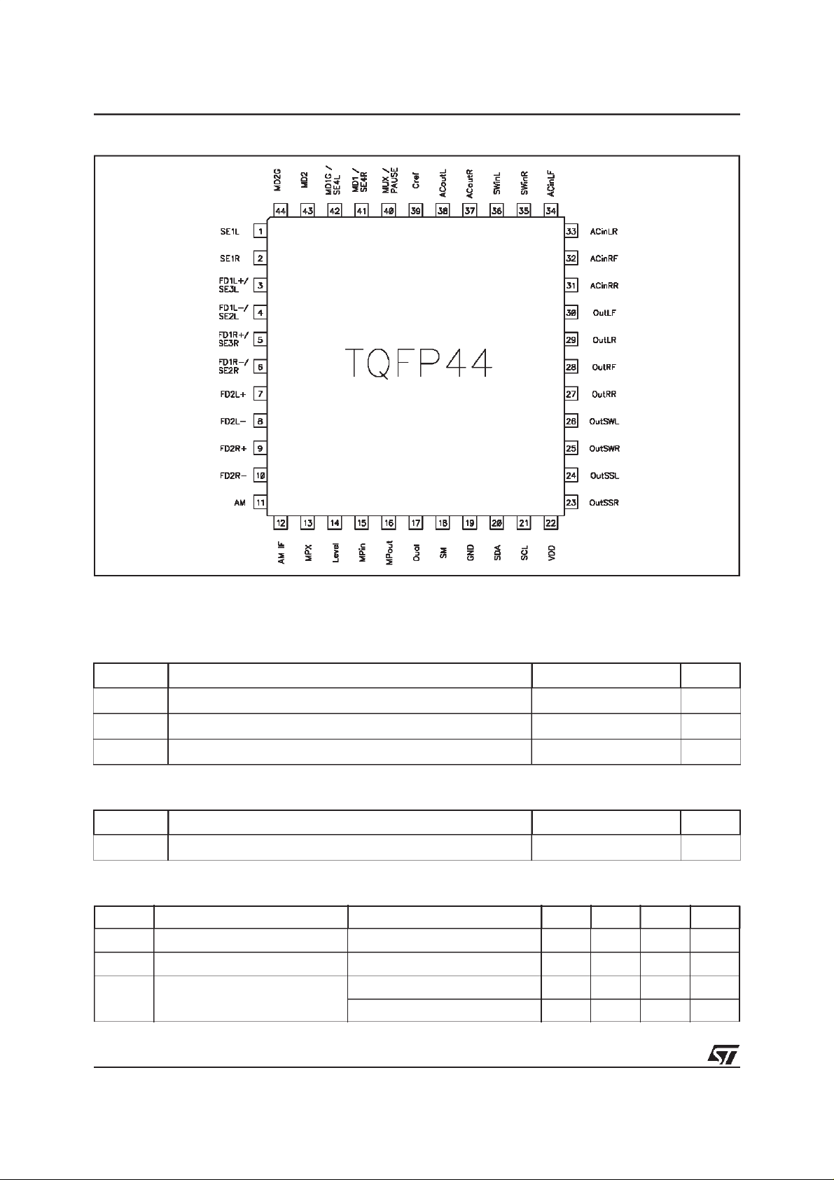
TDA7402
PIN CONNECTION (Top view)
ESD:
All pins are protected against ESD according to the MIL883 standard.
ABSOLUTEMAXIMUM RATINGS
Symbol Parameter Value Unit
T
V
amb
T
stg
Operating Supply Voltage 10.5 V
S
Operating Temperature Range -40 to 85 °C
Storage Temperature Range -55 to +150 °C
THERMAL DATA
Symbol Parameter Value Unit
R
th j-pins
Thermal Resistance Junction-pins max 65 °C/W
SUPPLY
Symbol Parameter Test Condition Min. Typ. Max. Unit
V
SVRR Ripple Rejection @ 1kHz Audioprocessor (allFilters flat) 60 dB
Supply Voltage 7.5 9 10 V
S
I
Supply Current VS=9V 50 mA
S
Stereodecoder + Audioprocessor 55 dB
2/59
Page 3

BLOCK DIAGRAM
TDA7402
3/59
Page 4

TDA7402
Audioprocessor Part Features:
Input Multiplexer 2 fully differential CD stereo inputs with programmable attenuation
1 single-ended stereo input
2 differential mono input
1 single-ended mono input
In-Gain 0..15dB, 1dB steps
internal Offset-cancellation (AutoZero)
separate second source-selector
Beep internal Beep with 4 frequencies
Mixing stage Beep, Phone and Navigation mixable to all speaker-outputs
Loudness programmable center frequency and frequency response
15 x 1dB steps
selectable flat-mode (constant attenuation)
Volume 0.5dB attenuator
100dB range
soft-step control with programmable times
Compander dynamic range compression for use with CD
2:1 compression rate
programmable max. gain
Bass 2nd order frequency response
center frequency programmable in 8 steps
DC gain programmable
+ 15 x 1dB steps
Treble 2nd order frequency response
center frequency programmable in 4 steps
+15 x 1dB steps
Voice Bandpass 2nd order butterworth highpass filter with programmable cut-off frequency
2nd order butterworth lowpass filter with programmable cut-off frequency
selectable flat-mode
Speaker 4 independent speaker controls in 1dB steps
control range 95dB
separate Mute
Subwoofer single-ended stereo output
independent stereo level controls in 1dB steps
control range 95dB
separate Mute
Mute Functions direct mute
digitally controlled SoftMute with 4 programmable mute-times
Pause Detector programmable threshold
4/59
Page 5

TDA7402
ELECTRICAL CHARACTERISTICS
VS= 9V; T
Symbol Parameter Test Condition Min. Typ. Max. Unit
INPUT SELECTOR
=25°C; RL=10kΩ; all gains = 0dB; f = 1kHz; unless otherwise specified
amb
R
V
S
G
IN MIN
G
IN MAX
G
STEP
V
V
offset
Input Resistance all single ended Inputs 70 100 130 kΩ
in
Clipping Level 2.2 2.6 V
CL
Input Separation 80 100 dB
IN
Min. Input Gain -1 0 +1 dB
Max. Input Gain 15 dB
Step Resolution 1 dB
DC Steps Adjacent Gain Steps 1 mV
DC
Remaining offset with AutoZero 0.5 mV
DIFFERENTIAL STEREO INPUTS
R
Input Resistance
in
(see Figure 1)
G
Gain only at true differential input 0 dB
CD
CMRR Common Mode Rejection Ratio V
RMS
to G
G
MIN
MAX
6mV
Differential 70 100 130 kΩ
-6 dB
-12 dB
CM
=1V
@ 1kHz 46 70 dB
RMS
e
Output-Noise @ Speaker-Outputs 20Hz - 20kHz, flat; all stages 0dB 9 µV
NO
DIFFERENTIAL MONO INPUTS
R
Input Impedance Differential 40 56 k
in
CMRR Common Mode Rejection Ratio V
BEEP CONTROL
V
f
Beep
RMS
Beep Level Mix-Gain = 6dB 350 mV
Beep Frequency f
MIXING CONTROL
M
LEVEL
Mixing Ratio Main / Mix-Source -6/-6 dB
V
CM
CM
V
CM
Beep1
f
Beep2
f
Beep1
f
Beep1
=1V
=1V
=1V
@ 10kHz 46 60 dB
RMS
@ 1kHz 40 70 dB
RMS
@ 10kHz 40 60 dB
RMS
600 Hz
780 Hz
1.56 kHz
2.4 kHz
Ω
5/59
Page 6

TDA7402
ELECTRICAL CHARACTERISTICS
(continued)
Symbol Parameter Test Condition Min. Typ. Max. Unit
G
A
MAX
A
STEP
MULTIPLEXER OUTPUT
R
R
C
V
Max. Gain 15 dB
MAX
Max. Attenuation -79 dB
Attennuation Step 1 dB
1
Output Impedance 225 Ω
OUT
Output Load Resistance 2 k
L
Output Load Capacitance 10 nF
L
DC Voltage Level 4.5 V
DC
LOUDNESS CONTROL
A
A
f
STEP
MAX
Peak
Step Resolution 1 dB
Max. Attenuation 19 dB
Peak Frequency f
P1
f
P2
f
P3
200 Hz
400 Hz
600 Hz
Ω
VOLUME CONTROL
G
A
MAX
A
STEP
E
E
V
Max. Gain 15.5 dB
MAX
Max. Attenuation 79.5 dB
Step Resolution 0.5 dB
Attenuation Set Error G = -20 to +20dB -0.75 0 +0.75 dB
A
Tracking Error 2dB
T
DC Steps Adjacent Attenuation Steps 0.1 3 mV
DC
SOFT MUTE
A
MUTE
T
Mute Attenuation 80 100 dB
Delay Time T1 0.48 ms
D
f
P4
800 Hz
G = -80 to -20dB -4 0 3 dB
From 0dB to G
MIN
0.5 5 mV
T2 0.96 ms
T3 123 ms
T4 324 ms
V
6/59
TH low
Low Threshold forSM-Pin
2
1V
Page 7
TDA7402
ELECTRICAL CHARACTERISTICS
(continued)
Symbol Parameter Test Condition Min. Typ. Max. Unit
V
TH high
R
V
Notes: 1. If configured as Multiplexer-Output
High Threshold for SM - Pin 2.5 V
Internal pull-up resistor 32 45 58 k
PU
Internal pull-up Voltage 3.3 V
PU
2. The SM-Pin is active low (Mute = 0)
BASS CONTROL
C
RANGE
A
STEP
Control Range +15 dB
Step Resolution 1 dB
Center Frequency f
f
C
C1
f
C2
f
C3
f
C4
f
C5
f
C6
f
C7
60 Hz
70 Hz
80 Hz
90 Hz
100 Hz
130 Hz
150 Hz
Ω
Q
DC
BASS
Quality Factor Q
Bass-DC-Gain DC = off 0 dB
GAIN
TREBLE CONTROL
C
RANGE
A
STEP
Control Range +15 dB
Step Resolution 1 dB
Center Frequency f
f
C
f
C8
1
Q
2
Q
3
Q
4
200 Hz
1
1.25
1.5
2
DC = on 4.4 dB
C1
f
C2
f
C3
f
C4
10 kHz
12.5 kHz
15 kHz
17.5 kHz
7/59
Page 8
TDA7402
ELECTRICAL CHARACTERISTICS
(continued)
Symbol Parameter Test Condition Min. Typ. Max. Unit
PAUSE DETECTOR
V
Zero Crossing Threshold Window 1 40 mV
TH
1
Window 2 80 mV
Window 3 160 mV
I
DELAY
V
Pull-Up Current 15 25 35 µA
Pause Threshold 3.0 V
THP
SPEAKER ATTENUATORS
R
G
A
MAX
A
STEP
A
MUTE
E
V
Input Impedance 35 50 65 kΩ
in
Max. Gain 15 dB
MAX
Max. Attenuation 79 dB
Step Resolution 1 dB
Output Mute Attenuation 80 90 dB
Attenuation Set Error 2dB
E
DC Steps Adjacent Attenuation Steps 0.1 5 mV
DC
Notes: 1. If configured as Pause-Output
AUDIO OUTPUTS
V
R
CLIP
R
C
V
Clipping Level d = 0.3% 2.2 2.6 V
Output Load Resistance 2 kΩ
L
Output Load Capacitance 10 nF
L
Output Impedance 30 120 W
OUT
DC Voltage Level 4.5 V
DC
VOICE BANDPASS
f
Highpass corner frequency f
HP
HP1
f
HP2
f
HP3
f
HP4
f
HP5
f
HP6
f
HP7
f
HP8
RMS
90 Hz
135 Hz
180 Hz
215 Hz
300 Hz
450 Hz
600 Hz
750 Hz
8/59
Page 9
TDA7402
ELECTRICAL CHARACTERISTICS
(continued)
Symbol Parameter Test Condition Min. Typ. Max. Unit
f
Lowpass corner frequency f
LP
LP1
f
LP2
3kHz
6kHz
SUBWOOFER ATTENUATORS
R
G
A
ATTN
A
STEP
A
MUTE
E
V
Input Impedance 35 50 65 k
in
Max. Gain 15 dB
MAX
Max. Attenuation 79 dB
Step Resolution 1 dB
Output Mute Attenuation 80 90 dB
Attenuation Set Error 2dB
E
DC Steps Adjacent Attenuation Steps 1 5 mV
DC
SUBWOOFER Lowpass
f
Notes: 1. If programmed as Subwoofer Diff.-Output
DIFFERENTIAL OUTPUTS
Lowpass corner frequency f
LP
1)
LP1
f
LP2
f
LP3
80 Hz
120 Hz
160 Hz
Ω
R
R
C
LMAX
C
DLMAX
V
Offset
R
V
e
load resistance at each output 1V
L
load resistance differential 1V
DL
Capacitive load at each output C
Capacitive load differential C
DC Offset at pins Output muted -10 10 mV
Output Impedance 30 Ω
OUT
DC Voltage Level 4.5 V
DC
Output Noise Output muted 6 µV
NO
COMPANDER
G
max. Compander Gain Vi < -46dB 19 dB
MAX
; ACcoupled; THD=1% 1 k
RMS
; ACcoupled; THD=1% 2 kΩ
2V
RMS
; ACcoupled; THD=1% 2 kΩ
RMS
; ACcoupled; THD=1% 4 k
2V
RMS
at each Output to Ground 10 nF
Lmax
between Output terminals 5 nF
Lmax
Vi < -46dB, Anti-Clip=On 29 dB
Ω
Ω
9/59
Page 10

TDA7402
ELECTRICAL CHARACTERISTICS
(continued)
Symbol Parameter Test Condition Min. Typ. Max. Unit
V
t
Att
t
Rel
REF
Attack time t
Release time t
Compander Reference Input-
Att1
t
Att2
t
Att3
t
Att4
Rel1
t
Rel2
t
Rel3
t
Rel4
V
REF1
6ms
12 ms
24 ms
49 ms
390 ms
780 ms
1.17 s
1.56 s
0.5 V
Level (equals 0dB)
C
Notes: 1. If programmed as Subwoofer Diff.-Output
Compression Factor Output Signal / Input Signal 0.5
F
V
V
REF2
REF3
1.0 V
2.0 V
GENERAL
RMS
RMS
RMS
e
Output Noise BW = 20Hz - 20kHz
NO
all gains = 0dB single endedinputs
S/N Signal to Noise Ratio all gains = 0dB
flat; V
O
=2V
RMS
bass, treble at +12dB;
a-weighted; V
V
IN
OUT
=1V
=1V
RMS
RMS
d distortion V
12dB
S
E
Channel Separation left/right 100 dB
C
TotalTracking Error AV= 0 to -20dB 0 1 dB
T
= -20 to -60dB 0 2 dB
A
V
output muted
10
3
µV
µV
106 dB
100 dB
= 2.6V
O
RMS
; all stages 0dB 0.005 %
; Bass & Treble =
0.05 %
10/59
Page 11

TDA7402
1.0 DESCRIPTION OF THE AUDIOPROCESSOR PART
1.1 Input stages
In the basic configuration two full-differential, two mono-differential, one single ended stereo and one singleended mono input are available. In addition a dedicated input for the stereodecoder MPX-signal is present.
Figure 1. Input-stages
Full-differential stereo Input 1 (FD1)
The FD1-input is implemented as a buffered full-differential stereo stage with 100kΩinput-impedance at each
input. The attenuation is programmable in 3 steps from 0 to -12dB in order to adapt the incoming signal level.
A 6dB attenuation is included in the differential stage, the additional 6dBare done by a following resistive divider. This input is also configurable as two single-ended stereo inputs (see pin-out).
Full-differential stereo Input 2 (FD2)
The FD2-input has the same general structure as FD1, but with a programmable attenuation of 0 or 6dB embedded in the differential stage.
11/59
Page 12

TDA7402
Mono-differential Input 1 (MD1)
The MD1-input is designed as a basic differential stage with 56kΩ input-impedance. This input is configurable
as a single-ended stereo input (see pin-out).
Mono-differential Input 2 (MD2)
The MD2-input has the same topology as MD1, but without the possibility to configure it to single ended.
Single-endedstereo Input (SE1), single-ended mono input (AM) and FM-MPX input
All single ended inputs offer an input impedance of 100kΩ. The AM-pin can be connected by software to the
input of the stereo-decoder in order to use the AM-noiseblanker and AM-High-Cut feature.
1.2 AutoZero
The AutoZero allows a reduction of the number of pins as well as external components by canceling any offset
generated by or before the In-Gain-stage (Please notice that externally generated offsets, e.g. generated
through the leakage current of the coupling capacitors, are not canceled).
The auto-zeroing is started every time the DATA-BYTE 0 is selected and needs max.
To avoidaudible clicks the Audioprocessor is muted before the loudness stage during this time. The AutoZerofeature is only present in the main signal-path.
0.3ms for the alignment.
AutoZero for Stereodecoder-Selection
A special procedure is recommended for selecting the stereodecoder at the main input-selector to guarantee
an optimum offset-cancellation:
(Step 0: SoftMute or Mute the signal-path)
Step 1: Temporary deselect the stereodecoder at all input-selectors
Step 2: Configure the stereodecoder via IIC-Bus
Step 3: Wait 1ms
Step 4: Select the stereodecoder at the main input-selector first
The root cause of this procedure is, that after muting the stereodecoder (Step 1), the internal stereodecoder
filters have to settle in order to perform a proper offset-cancellation.
AutoZero-Remain
In some cases, for example if the µP is executing a refresh cycle of the IIC-Bus-programming, it is not useful
to start a new AutoZero-action because no new source is selected and an undesired mute would appear at the
outputs. For such applications the A619 could be switched in the
dress-byte). If this bit is set to high, the DATABYTE 0 could be loaded without invoking the AutoZero and the
old adjustment-value remains.
AutoZero-Remain-Mode (Bit 6 of the subad-
1.3 Pause Detector / MUX-Output
The pin number 40(Pause/MUX) is configurable for two different functions:
1. During Pause-Detector OFF this pin is used as a mono-output of the maininput-selector. This signal is often
used to drive a level-/equalizer-display on the carradio front-panel.
2. DuringPause-Detector ON the pin isused todefine the time-constant ofthe detector by an externalcapacitor.
The pause-detector is driven by the internal stereodecoder-outputs in order to use pauses in the FM-signal
for alternate-frequency-jumps. If the signal-level of both stereodecoder channels is outside the programmed
voltage-window, the external capacitor is abruptly discharged. Inside the pause-condition the capacitor is
slowly recharged bya constant current of 25µA. The pause information is also available via IIC-Bus (see IICBus programming).
12/59
Page 13

1.4 Loudness
There are four parameters programmable in the loudness stage:
1.4.1 Attenuation
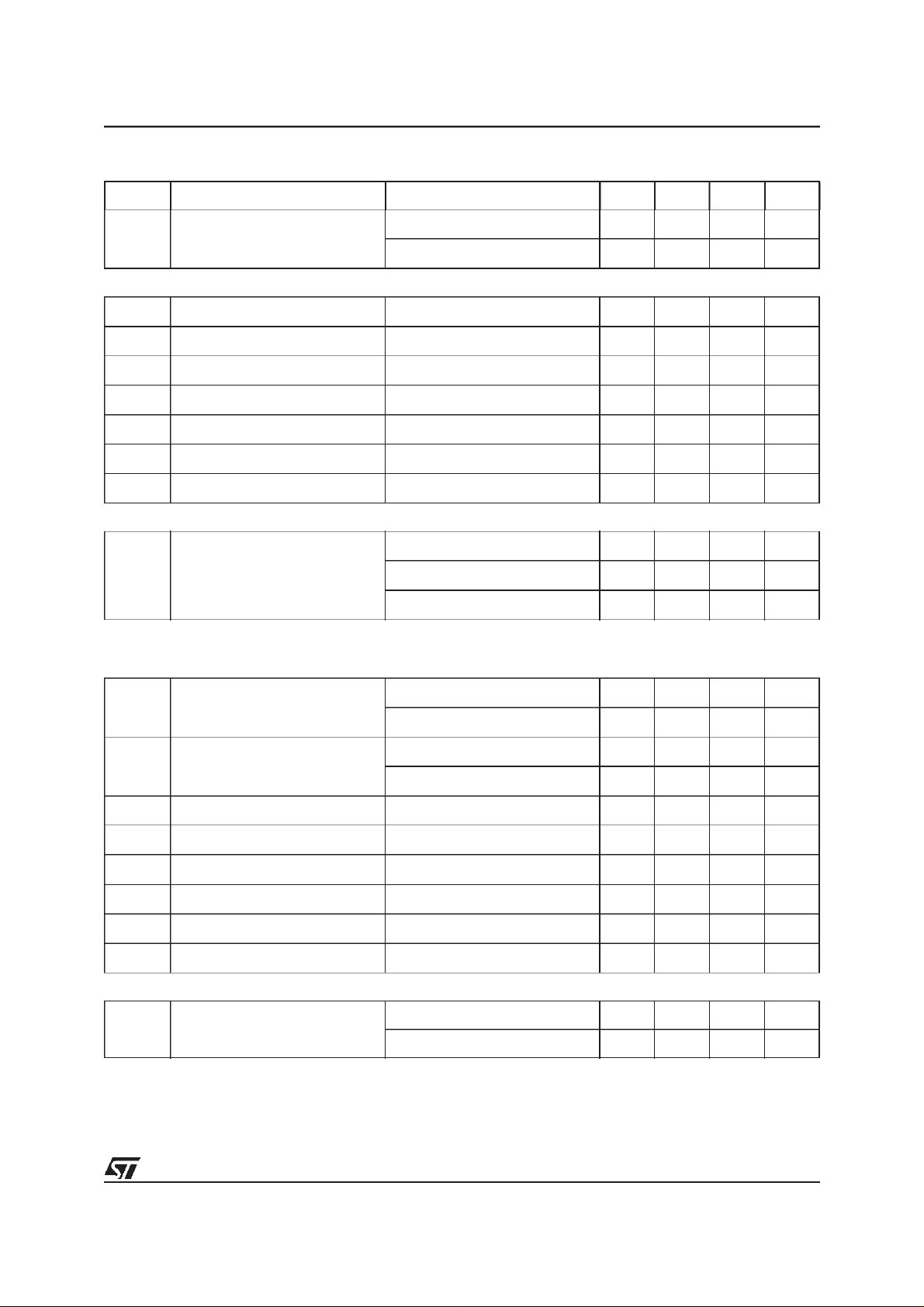
Figure 2 shows the attenuation as a function of frequency at fP= 400Hz
Figure 2. Loudness Attenuation @ fP= 400Hz.
0.0
-5.0
-10.0
dB
-15.0
-20.0
TDA7402
-25.0
10.0 100.0 1.0K 10.0K
Hz
1.4.2 Peak Frequency
Figure 3 shows the four possible peak-frequencies at 200, 400, 600 and 800HzFigure 3: Loudness Center frequencies @ Attn. = 15dB
Figure 3. Loudness Center frequencies @ Attn. = 15dB.
0.0
-5.0
dB
-10.0
-15.0
-20.0
10.0 100.0 1.0K 10.0K
Hz
13/59
Page 14

TDA7402
1.4.3 Loudness Order
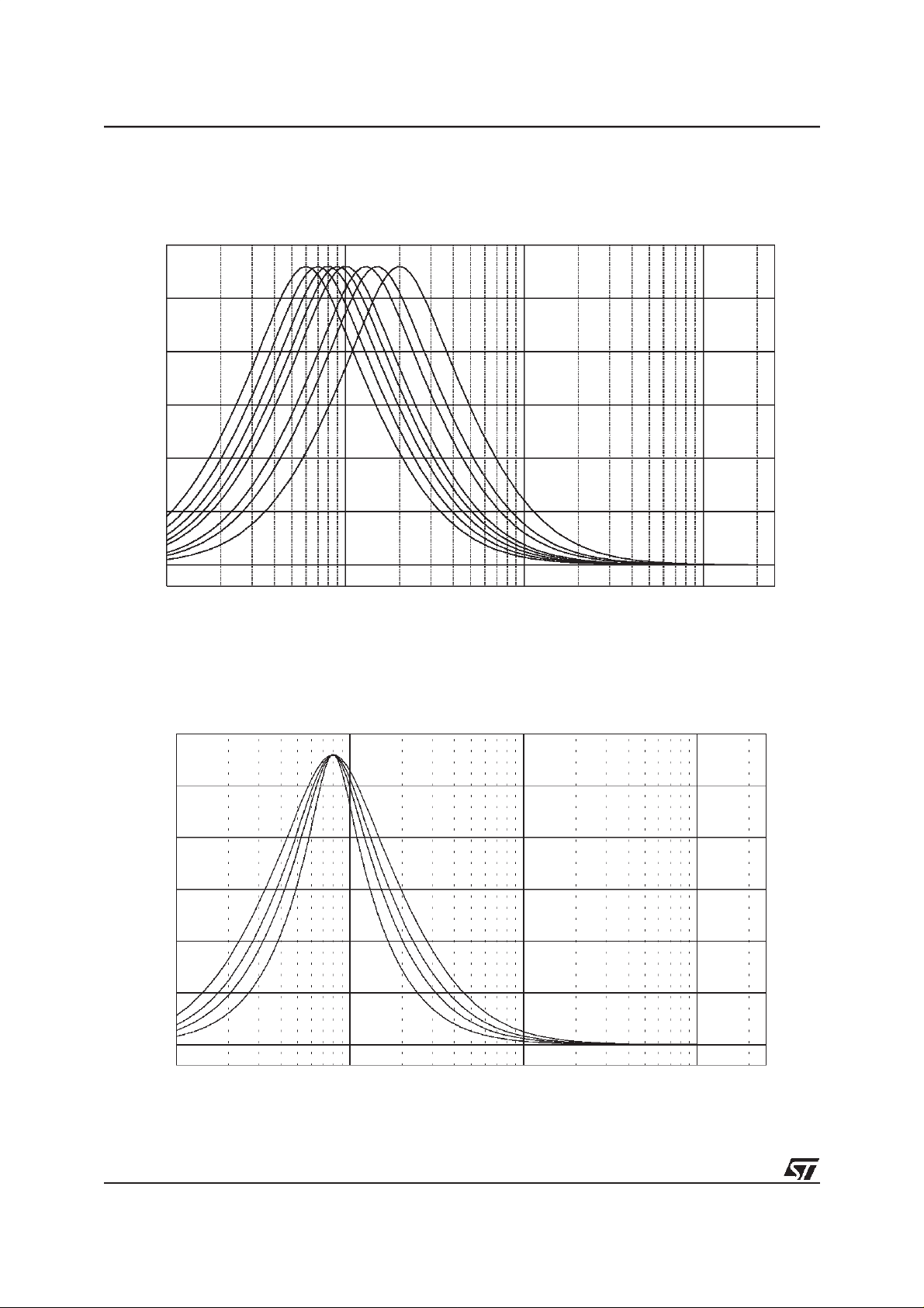
Different shapes of 1st and 2nd-Order Loudness
Figure 4. 1st and 2nd Order Loudness @ Attn. = 15dB, fP=400Hz
0.0
-5.0
dB
-10.0
-15.0
-20.0
10.0 100.0 1.0K 10.0K
1.4.4 Flat Mode
In flat mode the loudness stage works as a 0dB to -19dB attenuator.
Hz
1.5 SoftMute
The digitally controlled SoftMute stage allows muting/demuting the signal with a I2C-bus programmable slope.
The mute process can either be activated by the SoftMute pin or by the I
2
C-bus. This slope is realized in a spe-
cial S-shaped curve to mute slow in the critical regions (see Figure 5).
For timing purposes the Bit0 of the I
2
C-bus output register is setto 1 from the start ofmuting until the end of de-
muting.
Figure 5. Softmute-Timing
Note: Please notice that a started Mute-action is always terminated and could not be interrupted by a change of the mute -signal.
14/59
Page 15

TDA7402
1.6 SoftStep-Volume
When the volume-level is changed audible clicks could appear at the output. The root cause of those clicks
could either be a DC-Offset before the volume-stage or the sudden change of the envelope of the audiosignal.
With the SoftStep-feature both kinds of clicks could be reduced to a minimum and are no more audible. The
blend-time from one step to the next is programmable in four steps.
Figure 6. SoftStep-Timing
1dB
0.5dB
SS Time
-0.5dB
-1dB
Note: For steps more than 0.5dB theSoftStep mode should bedeactivated because it could generate a hard 1dB stepduring the blend-time.
1.7 Bass
There are four parameters programmable in the bass stage:
1.7.1 Attenuation
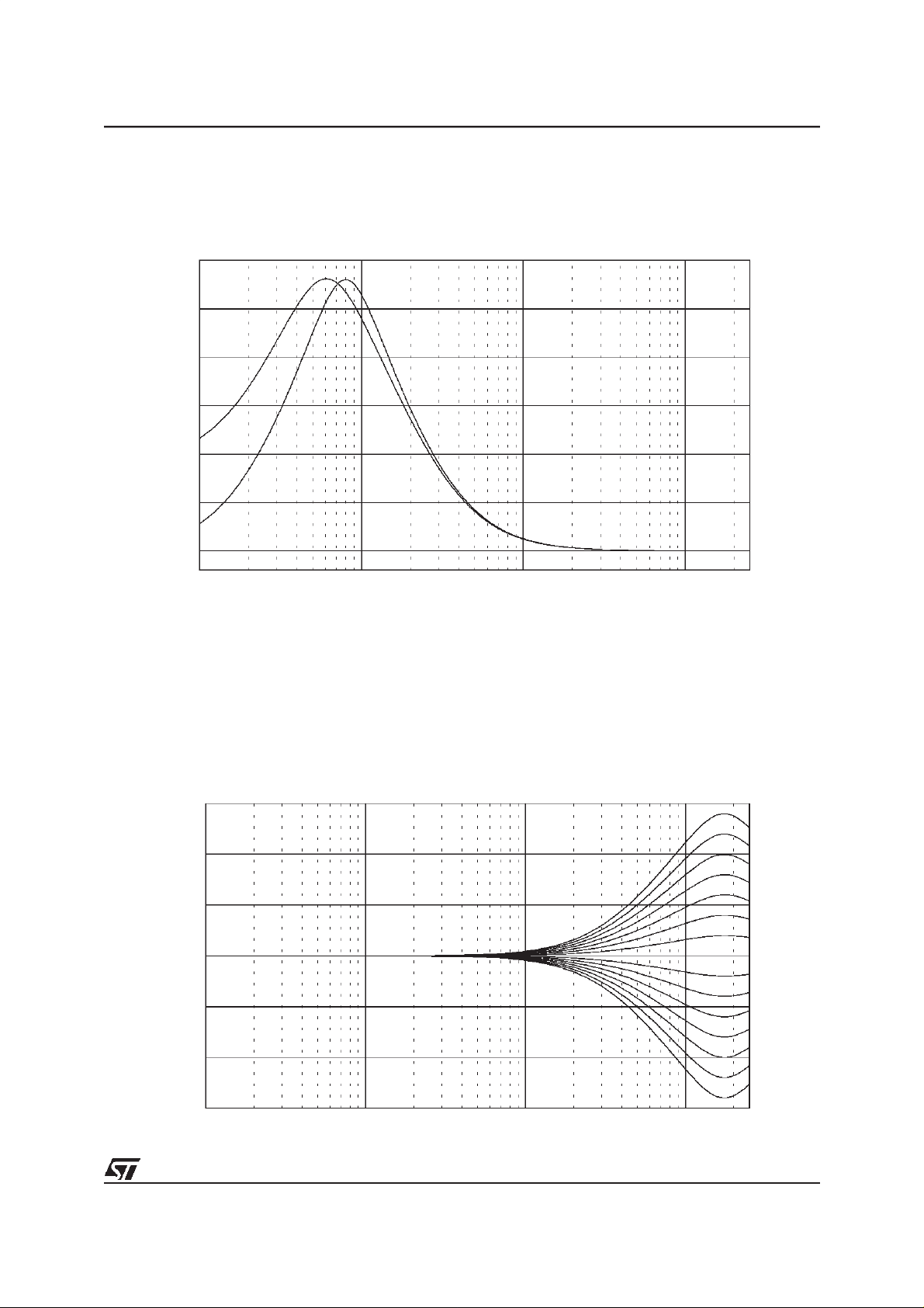
Figure 7 shows the attenuation as a function of frequency at a center frequency of 80Hz.
Figure 7. Bass Control @ fC= 80Hz, Q = 1
15.0
10.0
5.0
dB
0.0
-5.0
-10.0
-15.0
10.0 100.0 1.0K 10.0K
Hz
15/59
Page 16
TDA7402
1.7.2 Center Frequency
Figure 8 shows the eight possible center frequencies 60, 70, 80, 90, 100, 130, 150 and 200Hz.
Figure 8. Bass center Frequencies @ Gain = 14dB, Q = 1
15.0
12.5
10.0
7.5
dB
5.0
2.5
0.0
10.0 100.0 1.0K 10.0K
Hz
1.7.3 Quality Factors
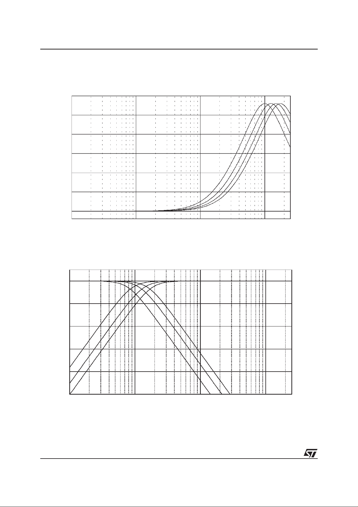
Figure 9 shows the four possible quality factors 1, 1.25, 1.5 and 2.
Figure 9. Bass Quality factors @ Gain = 14dB, fC= 80Hz
15.0
12.5
10.0
7.5
5.0
2.5
0.0
16/59
10.0 100.0 1.0K 10.0K
Page 17
TDA7402
1.7.4 DC Mode
In this mode the DC-gainis increased by 4.4dB. In addition the programmed center frequency and quality factor
is decreased by 25% which can be used to reach alternative center frequencies or quality factors.
Figure 10. Bass normal and DC Mode @ Gain = 14dB, fC= 80Hz
15.0
12.5
10.0
7.5
5.0
2.5
0.0
10.0 100.0 1.0K 10.0K
Note: The center frequency, Q and DC-mode can be set fully independently.
1.8 Treble
There are two parameters programmable in the treble stage:
1.8.1 Attenuation
Figure 11 shows the attenuation as a function of frequency at a center frequency of 17.5kHz.
Figure 11. Treble Control @ fC= 17.5kHz
15.0
10.0
5.0
0.0
-5.0
-10.0
-15.0
10.0 100.0 1.0K 10.0K
17/59
Page 18
TDA7402
1.8.2 Center Frequency
Figure 12 shows the four possible center frequencies 10k, 12.5k, 15k and 17.5kHz.
Figure 12. Treble Center Frequencies @ Gain = 14dB
15.0
12.5
10.0
7.5
5.0
2.5
0.0
10.0 100.0 1.0K 10.0K
1.9 Subwoofer Application
Figure 13. Subwoofer Application with LPF 80/120/160Hz and HPF 90/135/180Hz
0.0
-10.0
-20.0
dB
-30.0
-40.0
-50.0
10.0 100.0 1.0K 10.0K
Hz
Both filters, the lowpass- as well as the highpass-filter, have butterworth characteristic so that their cut-off frequencies are not equal but shifted by the factor 1.125 to get a flat frequency response.
18/59
Page 19

1.10Voice-Band Application
Figure 14. VoiceBand Application with HPF 300/450/600/750Hz and LPF 3k/6kHz
0.0
-10.0
-20.0
dB
-30.0
-40.0
-50.0
10.0 100.0 1.0K 10.0K
Hz
TDA7402
19/59
Page 20

TDA7402
1.11Compander
Signal-Compression
A fully integrated signal-compressor with programmable Attack- and Decay-times is present in the A619 (see
Figure 15).
The compander consists of a signal-level detection, an A/D-Converter plus adder and the normal SoftStep-Volume-stage. Firstof all the left and the right InGain-signal is rectified, respectively, andthe logarithm isbuild from
the summed signal. The following low-pass smooth the output-signal of the logarithm-amplifier and improves
the low-frequency suppression. The low-pass output-voltage then isA/D-converted an added tothe current volume-word defined by the IIC-Bus. Assuming reference-level or higher at thecompander input,the output of the
ADC is 0. At lower levels the voltage is increasing with 1Bit/dB. It is obvious that with this configuration and a
0.5dB-step volume-stage the compression rate is fixed to 2:1 (1dB less at the input leads to 0.5dB less at the
output).
The internal reference-level of the compander is programmable in three steps from 0.5V
RMS
to 2V
proper behavior of the compression-circuit it is mandatory to have at a 0dB input-signal exactly the programmed
reference-level after the InGain-stage. E.g. ata configured reference-level of 0.5V
stage has to have also 0.5V
at 0dB source-signal (Usually the 0dB for CD is defined as the maximum pos-
RMS
the output of theInGain-
RMS
sible signal-level). To adapt the external level to the internal reference-level the programmable attenuation in
the differential-stages and the InGain can be used.
Figure 15. Compander Block Diagram
RMS
. For a
Anti-Clipping
In a second application the compander-circuit can be used for a Anti-Clipping or Limiting function. In this case
one of the dedicated inputs(AM or MPin) is connected directly to the Clip-Detector of the Power-Amplifier. If no
clipping is detected, the open-collector output of the Power-Amplifier is highohmic and the input-voltage of the
rectifier is V
. The level-detector interprets this as a very small signal and reacts with the maximum pro-
REF
grammed compander-gain. In the application this gain has to be compensated by decreasing the volume with
20/59
Page 21

TDA7402
the same valuein order to get the desired output-level. Inclipping situation the open-collector-current generates
a voltage-drop at the rectifier-input, which forces the compander to decrease the gain until the clipping disappears.
It is even possible to run the compression-mode and the Anti-Clipping mode in parallel. In this case the maximum Compander-Gain should be set to 29dB.
1.11.1Characteristic
To achieve the desired compression characteristic like shown below the volume has to be decreased by 4dB.
Figure 16. Compander Characteristic
1.11.2I C -BUS-Timing
During the Compander is working a volumeword coming from this stage is added t o the
2
C-Bus volum e-word and the volume is
I
changed with a soft slope between adjacent
steps (S oftStep-stage). As mentioned in the
description of this stage it is not recommended tochange the volume during thisslope. To
avoid this while the Compander is working
Output Level
dB
-10
-20
-30
-40
0
-8dB
2:1
-38dB
15dB
and the volume has to be changed, the com-
-50
pander-hold-bit is implemented (Bit 7 in the
subaddress-byte). The recommended timing
-60
0 -10 -20 -30 -40 -50 -60
Input Level
dB
for changing the volume during c ompanderON is the following:
1. Set the compander-hold-bit
2. Wait theactual SoftStep-time
3. Change the volume
4. Reset the compander-hold-bit
The SoftStep-times are i n compander-ON condition automatically adapted to the attack-time of the Compander.
In the following table the related SoftStep-times are shown:
Attack-Time SoftStep-Time
6ms 0.16ms
12ms 0.32ms
24ms 0.64ms
48ms 1.28ms
1.12AC-Coupling
In some applications additional signal manipulations are desired, for example surround-sound or more-bandequalizing. For this purpose an AC-Coupling is placed before the speaker-attenuators, which can be activated
or internally shorted by
AC-Outputs. The input-impedance of this AC-Inputs is 50k
I
C-Bus. In short condition the input-signal of the speaker-attenuator is available at the
.
Ω
21/59
Page 22

TDA7402
1.13Output Selector
The output-selector allows to connect the main- orthe second-source to the Front-, Rearand Subwoofer speaker-attenuator, respectively. As an example of this programming the device is able to connect via software the
main-source to theback (rear) and the second-source to thefront (seeFigure 17). In addition to this stageallows
to setup different applications by IIC-Bus programming. In figure 18 to 20 three examples are given.
Figure 17. Output Selector
1.14Subwoofer
Several different applications are possible with the Subwoofer-circuit:
1. Subwoofer-Filter OFF
a. Main-source stereo (AC-coupled)
b. Second-source stereo (DC-coupled)
c. Main-source mono-differential (DC-coupled)
d. Second-source mono-differential (DC-coupled)
2. Subwoofer-Filter ON
a. Main-source mono-differential (DC-coupled)
b. Second-source mono-differential (DC-coupled)
c. Center-Speaker-Mode (filtered mono signal at SWL, unfiltered mono signal at SWR)
In all applications the phase of the output-signal can be configured to be 0° or 180° . In the Center-SpeakerMode only at the filtered output the phase is changed.
22/59
Page 23

Figure 18. Application1 using internal Highpass- and mono Low-pass-Filter
TDA7402
Figure 19. Application2 using internal Highpass- and external stereo Low-pass-Filter
23/59
Page 24

TDA7402
Figure 20. Application3 using pure external Filtering (e.g. DSP)
1.15Speaker-Attenuator and Mixing
A Mixing-stage is placed after each speaker-attenuator and can beset independly to mixing-mode. Having a full
volume for the Mix-signal the stage offers a wide flexibility to adapt the mixing levels.
Figure 21. Output Selector
24/59
Page 25

TDA7402
1.16Audioprocessor Testing
During the Testmode, which can be activated by setting bit D0of the stereodecoder testing-byteand the audioprocessor testing byte, several internal signals are available at the FD2R- pin. During this mode the input resistance of 100kOhm is disconnected from the pin. The internal signals available are shown in the Data-byte
specification.
2.0 STEREODECODER PART
2.1 FEATURES:
■
no external components necessary
■ PLL with adjustment free, fully integrated VCO
■
automatic pilot dependent MONO/STEREO switching
■
very high suppression of intermodulation and interference
■
programmable Roll-Off compensation
■ dedicated RDS-Softmute
■
Highcut- and Stereoblend-characterisctics programmable in a wide range
■
FM/AMNoiseblanker with several threshold controls
■ Multipath-detector with programmable internal/external influence
■
I2C-bus control of all necessary functions
2.2 ELECTRICAL CHARACTERISTICS
VS= 9V, deemphasis time constant = 50µs, MPX input voltage V
frequency = 1kHz, input gain = 6dB, T
Symbol Parameter Test Condition Min. Typ. Max. Unit
V
R
G
G
G
SVRR Supply Voltage Ripple Rejection V
THD Total Harmonic Distortion f
S+N
MPX Input Level Input Gain = 3.5dB 0.5 1.25 V
in
Input Resistance 100 k
in
Min. Input Gain 3.5 dB
min
Max. Input Gain 11 dB
max
Step Resolution 2.5 dB
step
a Max. Channel Separation 50 dB
Signal plus Noise to Noise Ratio A-weighted, S = 2V
=27°C, unless otherwise specified.
amb
= 100mV, f = 1kHz 60 dB
ripple
=1kHz, mono 0.02 0.3 %
in
rms
N
MONO/STEREO-SWITCH
V
PTHST1
Pilot Threshold Voltage for Stereo, PTH = 1 15 mV
= 500mV (75kHz deviation), modulation
MPX
91 dB
rms
Ω
V
PTHST0
V
PTHMO1
Pilot Threshold Voltage for Stereo, PTH = 0 25 mV
Pilot Threshold Voltage for Mono, PTH = 1 12 mV
25/59
Page 26

TDA7402
2.2 ELECTRICAL CHARACTERISTICS
(continued)
Symbol Parameter Test Condition Min. Typ. Max. Unit
V
PTHMO0
Pilot Threshold Voltage for Mono, PTH = 0 19 mV
PLL
f/f Capture Range 0.5 %
∆
DEEMPHASIS and HIGHCUT
τ
DeempFM
M
FM
τ
DeempAM
M
AM
Deemphasis Timeconstants FM V
V
V
V
HighcutTimeconstantMultiplierFM V
Deemphasis Timeconstants AM V
V
V
V
HighcutTimeconstantMultiplierAM V
LEVEL
LEVEL
LEVEL
LEVEL
LEVEL
LEVEL
LEVEL
LEVEL
LEVEL
LEVEL
>> V
>> V
>> V
>> V
<< V
>> V
>> V
>> V
>> V
<< V
HCH
HCH
HCH
HCH
HCL
HCH
HCH
HCH
HCH
HCL
50 µs
62.5 µs
75 µs
100 µs
3
37.5 µs
47 µs
56 µs
75 µs
3.7
REF5V Internal Reference Voltage 5 V
L
L
maxs
L
Gstep
VSBL
VSBL
VSBL
VHCH
VHCH
VHCH
VHCL
VHCL
VHCL
min. LEVEL Gain 0 dB
min
max. LEVEL Gain 6 dB
LEVEL Gain Step Resolution see section 2.7 0.4 dB
Min. Voltage for Mono see section 2.8 20 %REF5V
min
Max. Voltage for Mono see section 2.8 70 %REF5V
max
Step Resolution see section 2.8 3.3 %REF5V
step
Min. Voltage for NO Highcut see section 2.9 42 %REF5V
min
Max. Voltage for NO Highcut see section 2.9 66 %REF5V
max
Step Resolution see section 2.9 8.4 %REF5V
step
Min. Voltage for FULL High cut see section 2.9 17 %VHCH
min
Max. Voltage for FULL High cut see section 2.9 33 %VHCH
max
Step Resolution see section 2.9 4.2 %REF5V
step
Carrier and harmonic suppression at the output
α19 Pilot Signal f=19kHz 50 dB
α38 Subcarrier f=38kHz 75 dB
26/59
Page 27

TDA7402
2.2 ELECTRICAL CHARACTERISTICS
Symbol Parameter Test Condition Min. Typ. Max. Unit
57 Subcarrier f=57kHz 62 dB
α
76 Subcarrier f=76kHz 90 dB
α
Intermodulation (Note 2.3.1)
2f
α
3f
α
Traffic Radio (Note 2.3.2)
57 Signal f=57kHz 70 dB
α
SCA - Subsidiary Communications Authorization (Note 2.3.3)
α67 Signal f = 67kHz 75 dB
ACI - Adjacent Channel Interference (Note 2.3.4)
α114 Signal f=114kHz 95 dB
α190 Signal f=190kHz 84 dB
=10kHz, f
mod
=13kHz, f
mod
=1kHz 65 dB
spur
=1kHz 75 dB
spur
(continued)
2.3 NOTES TO THE CHARACTERISTICS
2.3.1 Intermodulation Suppression
α2
α3
VOsign al()at1kHz()
-------------- ------------------- ---------- -------------- ------ - fs; 2 10kHz⋅()19kHz–==
()
V
spurious
O
V
sig nal()at1kHz()
O
----------------- --------------- --------- --------------- ------- - fs;
V
spuri ous()at1kHz()
O
()
at1kHz
313kHz⋅()38kHz
–==
measured with: 91% pilot signal; fm = 10kHz or 13kHz.
2.3.2 Traffic Radio (V.F.) Suppression
α57 V.W.F()
------------------- -------------- -------- --------------- -------------- --------------- --- -=
V
O
()
V
signal
O
spurious()at1kHz 23kHz±()
()
at1kHz
measured with: 91% stereo signal; 9% pilot signal; fm=1kHz; 5% subcarrier (f=57kHz, fm=23Hz AM, m=60%)
2.3.3 SCA ( Subsidiary Communications Authorization )
VOsig nal()at1kHz()
α 67
----------------- --------------- -------- -------------- --------- -
V
spuri ous()at1kHz()
O
;
f
238kHz⋅()67kHz
s
–==
measured with: 81% mono signal; 9% pilot signal; fm=1kHz; 10%SCA - subcarrier ( fS= 67kHz, unmodulated ).
27/59
Page 28

TDA7402
2.3.4 ACI ( Adjacent Channel Interference )
VOsignal()at1kHz()
α114
α190
measured with: 90% mono signal; 9% pilot signal; fm=1kHz; 1% spurious signal ( fS= 110kHz or 186kHz, unmodulated).
2.4 NOISE BLANKER PART
2.4.1 Features:
■ AM and FM mode
■
internal 2nd order 140kHz high-pass filter for MPX path
■
internal rectifier and filters for AM-IF path
■
programmable trigger thresholds
■ trigger threshold dependent on high frequency noise with programmable gain
■
additional circuits for deviation- and fieldstrength-dependent trigger adjustment
■
4 selectable pulse suppression times for each mode
■ programmable noise rectifier charge/discharge current
----------------- --------------- -------- -------------- --------- -f
()
V
spuri ous
O
VOsignal()at1kHz()
----------------- --------------- -------- -------------- --------- -f
()
V
spuri ous
O
()
at4kHz
()
at4kHz
; 110kHz 3 38kHz⋅()–==
; 186kHz 5 38kHz⋅()–==
s
s
2.4.2 ELECTRICAL CHARACTERISTICS
All parameters measured in FM mode if not otherwise specified.
Symbol Parameter Test Condition Min. Typ. Max. Unit
V
V
TRNOISE
V
RECT
TR
Trigger Threshold
1)
noise controlled
Trigger Threshold
Rectifier Voltage V
meas.with
V
=0.9V
PEAK
111 30 mV
110 35 mV
101 40 mV
100 45 mV
011 50 mV
010 55 mV
001 60 mV
000 65 mV
meas.with
V
=1.5V
PEAK
00 260 mV
01 220 mV
10 180 mV
11 140 mV
=0mV 0.9 V
MPX
V
=50mV,f=150kHz 1.7 V
MPX
V
=200mV, f=150kHz 3.5 V
MPX
OP
OP
OP
OP
OP
OP
OP
OP
OP
OP
OP
OP
28/59
Page 29

TDA7402
2.4.2 ELECTRICAL CHARACTERISTICS (continued)
Symbol Parameter Test Condition Min. Typ. Max. Unit
V
RECT
V
RECTFS
T
SFM
T
SAM
V
RECTADJ
SR
V
ADJMP
R
AMIF
G
AMIF,min
G
AMIF,max
G
AMIF,step
f
AMIF,min
f
AMIF,max
Deviation dependent
DEV
Rectifier Voltage
meas.with
V
=500mV
MPX
(75kHz dev.)
11
10
01
00
0.9
(off)
1.2
2.0
2.8
Fieldstrength
controlled Rectifier
Voltage
meas.with
V
=0mV,
MPX
<< V
V
LEVEL
(fully mono)
SBL
11
10
01
00
0.9
(off)
1.4
1.9
2.4
Suppression Pulse Duration FM Signal HOLDN in
Testmode
Suppression Pulse Duration AM Signal HOLDN in
Testmode
Noise rectifier discharge
adjustment
Noise rectifier
PEAK
charge
Noise rectifier adjustment
through
Signal PEAK in
Testmode
Signal PEAK in
Testmode
Signal PEAK in
Testmode
Multipath
00
01
10
11
00
01
10
11
00
01
10
11
0
1
00
01
10
11
38
25.5
32
22
1.2
800
1.0
640
0.3
0.8
1.3
2.0
10
20
0.3
0.5
0.7
0.9
AM IF Input resistance 35 50 65 kOhm
min. gain AM IF Signal AM-RECTIFIERin
max. gain AM IF 20 dB
Testmode
6dB
step gain AM IF 2 dB
min. fcAM IF Signal AM-RECTIFIERin
max. fcAM IF 56 kHz
Testmode
14 kHz
mV/µs
V
OP
V
OP
V
OP
V
OP
V
V
V
V
µs
µs
µs
µs
ms
µs
µs
µs
V/ms
V/ms
Notes: 1. All thresholds are measured using a pulse with TR=2µs,T
PEAK voltage.
V
in
V
op
DC
T
T
R
HIGH
=2µs and TF=10µs. The repetition rate must not increase the
HIGH
T
F
Time
29/59
Page 30

TDA7402
Figure 22. Trigger Threshold vs. V
VTH
65mV
8STEPS
30mV
PEAK
MIN. TR IG. THR ESH OLD NOISE C ON TR OLLED TRIG. THRE S HO LD
1.5V0.9V
Figure 23. Fig. 23: Deviation Controlled Trigger Adjustment
V
PEAK
[V ]
OP
260m V (00)
220m V (01)
180m V (10)
140m V (11)
V
PEAK [V]
00
2.8
2.0
1.2
0.9
20 32.5 45 75
Figure 24. Fieldstrength Controlled Trigger Adjustment
V
PEAK
MONO STEREO
3V
≈
2.4V ( 00)
1.9V (01 )
NOISE
ATC_SB OFF (11)
1.4V (10 )
01
10
Detector off (11)
DEVIATION [KHz]
0.9V
30/59
noisy s ignal good signal
E’
Page 31

TDA7402
2.5 MULTIPATH Detector
2.5.1 Features:
■
internal 19kHz band-pass filter
■ programmable band-pass- and rectifier-gain
■
selectable internal influence on Stereoblend and/or Highcut
2.5.2 ELECTRICAL CHARACTERISTICS
Symbol Parameter Test Condition Min. Typ. Max. Unit
f
CMP
Center frequency of MultipathBandpass
G
BPMP
G
RECTMP
Bandpass Gain G1 6 dB
Rectifier Gain
I
CHMP
I
DISMP
Rectifier Charge Current 0.25
Rectifier Discharge Current 4 mA
QUALITY DETECTOR
A
Multipath Influence Factor
stereodecoder locked on Pilottone 19 kHz
G2 12 dB
G3 16 dB
G4 18 dB
G1 7.6 dB
G2 4.6 dB
G3 0 dB
µA
0.5
00
01
10
11
0.70
0.85
1.00
1.15
31/59
Page 32

TDA7402
3.0 FUNCTIONAL DESCRIPTION OF STEREODECODER
Figure 25. Block diagram of Stereodecoder
The stereodecoder-part of theA619 (see Fig. 25) contains all functions necessary to demodulate the MPX-signal like pilottone-dependent MONO/STEREO-switching aswell as ”stereoblend” and ”highcut”. Adaptations like
programmable input gain, roll-off compensation, selectable deemphasis time constant and a programmable
fieldstrength input allow to use different IF-devices.
3.1 Stereodecoder-Mute
The A619 has a fastandeasy to control RDS-Mute function which is a combination of the audioprocessor’s SoftMute and the high-ohmic mute of the stereodecoder. If the stereodecoder isselected and a SoftMute command
is sent (oractivated through the SM-pin)the stereodecoder will be set automatically to the high-ohmic mute condition after the audio-signal has been softmuted. Hence a checkingof alternate frequencies could be performed.
Additionally the PLL can be set to ”Hold”-mode, which disables the PLL input during the mute time. To release
the system from the mute condition simply the unmute-command must be sent: the stereodecoder is unmuted
immediately andtheaudioprocessor is softly unmuted. Fig. 26 shows the output-signal V
stereodecoder mutesignal. This influence of SoftMute onthe stereodecoder mute canbeswitched off bysetting
bit 3 of the SoftMute byte to ”0”. A stereodecoder mute command (bit 0, stereodecoder byte set to ”1”) willset
the stereodecoder
If any other source than the stereodecoder is selected the decoder remains muted and the MPX-pin is connected to V
should be applied.
to avoid any discharge of the coupling capacitor through leakage currents. No further mute command
ref
in anycase
independently to the high-ohmic mute state.
aswell astheinternal
O
32/59
Page 33

Figure 26. Signals during stereodecoder’s SoftMute
Figure 27. Signal-Control via SoftMute-Pin
TDA7402
3.2 InGain + Infilter
The InGain stage allows to adjust the MPX-signal to a magnitude of about 1V
mended value. The 4.th order input filter has a corner frequency of 80kHz and is used to attenuate spikes and
noise and acts as an anti-aliasing filter for the following switch capacitor filters.
internally which is the recom-
rms
3.3 Demodulator
In the demodulator block the left and the right channel are separated from the MPX-signal. In this stage also the
19-kHz pilottoneis cancelled. Forreaching a high channel separation the A619 offers anI
roll-off adjustment which is able to compensate the lowpass behavior of the tuner section. If the tuner’s attenuation at 38kHz is in a range from 7.2% to 31.0% the A619 needs no external network in front of the MPX-pin.
Within this range an adjustment to obtain at least 40dB channel separation is possible. The bits for this adjustment are located together with the fieldstrength adjustment in one byte. This gives thepossibility to perform an
2
C-bus programmable
33/59
Page 34

TDA7402
optimization step during the production of the carradio where the channel separation and the fieldstrength control are trimmed. The setup of the Stereoblend characteristics which is programmable in a wide range is described in 2.8.
3.4 Deemphasis and Highcut
The deemphasis-lowpass allows to choose a time constant between 37.5 and 100µs. The highcut control range
will be 2 xτ
D7 of the hightcut-byte will shift timeconstant and range.
Inside the highcut control range (between VHCH and VHCL) the LEVEL signal is converted into a 5 bit word
which controls the lowpass timeconstant between τ
always 5 bits independently of the absolute voltage range between the VHCH- and VHCL-values. In addition
the maximum attenuation can be fixed between 2 and 10dB.
The highcut function can be switched off by I
The setup of the highcut characteristics is described in 2.9.
3.5 PLL and Pilottone-Detector
The PLL has the task to lock on the 19kHz pilottone during a stereo-transmission to allow a correct demodulation. The included pilottone-detector enables the demodulation if the pilottone reaches the selected pilottone
threshold V
gram) can be checked by reading the status byte of the A619 via I
set into”Hold”-mode which freezes the PLL’s state(bit D
will again follow the input signal only by correcting the phase error.
or 2.7 x τ
Deemp
. Two different thresholds are available. The detector output (signal STEREO, see Blockdia-
PTHST
dependent on the selected time constant (see programming section). The bit
Deemp
...3 (3.7) x τ
Deemp
2
C-bus (bit D7, Highcut byte set to ”0”).
2
, Softmute byte). After releasing the Softmute the PLL
4
. Thereby the resolution will remain
Deemp
C-bus. During a Softmute the PLL can be
3.6 Fieldstrength Control
The fieldstrength input is used tocontrol the highcut- and the stereoblend-function. In addition the signalcan be
also used to control the noiseblanker thresholds and as input for the multipath detector. These additional functions are described in sections 3.3 and 4.
3.7 EVEL-Input and -Gain
To suppress undesired high frequency modulation on the highcut- and stereoblend-control signal the LEVEL
signal islowpass filtered firstly. The filter is a combination of a 1.st-orderRC-lowpass at 53kHz (working as antialiasing filter)anda1.st-order switched-capacitor-lowpass at 2.2kHz. The second stageis aprogrammable gain
stage to adapt the LEVEL signal internally to different IF-devices (see Testmode section 5: LEVELHCC). The
gain is widely programmable in 16 steps from 0dB to 6dB (step=0.4dB). These 4 bits are located together with
the Roll-Off bits inthe ”Stereodecoder-Adjustment”-byte to simplify a possible adjustment duringthe production
of the carradio. This signal controls directly the Highcut stage whereas the signal is filtered again (fc=100Hz)
before the stereoblend stage (see fig. 32).
3.8 Stereoblend Control
The stereoblend control block converts the internal LEVEL-voltage (LEVELSB) into an demodulator compatible
analog signal which is used to control the channel separation between 0dB and the maximum separation. Internally this control range hasa fixed upper limit which is the internal reference voltage REF5V. The lower limitcan
be programmed between 20 and 70% of REF5V in 3.3% steps (see figs.28, 29).
To adjust the external LEVEL-voltage to the internal range two values must be defined: the LEVEL gain L
and
G
VSBL (see fig. 29). At the point of full channel separation the external level signal has to be amplified that internally it becomes equal to REF5V. The second point (e.g. 10dB channel sep.) is then adjusted with the VSBL
voltage.
34/59
Page 35

TDA7402
Figure 28. Internal stereoblend characteristics
The gain can be programmed through 4bits in the ”Stereodecoder-Adjustment”-byte. All necessary internal reference voltages like REF5V are derived from a bandgap circuit. Therefore they have a temperature coefficient
near zero.
Figure 29. Relation between internal and external LEVEL-voltages for setup of Stereoblend
70
20
3.9 Highcut Control
The highcut control set-up is similar to the stereoblend control set-up : the starting point VHCH can be set with
2 bits to be 42, 50, 58 or 66% of REF5V whereas the range can be set to be 17, 22, 28 or 33% of VHCH (see
fig. 30).
Figure 30. Highcut characteristics
35/59
Page 36

TDA7402
4.0 FUNCTIONAL DESCRIPTION OF THE NOISEBLANKER
In the automotive environment the MPX-signal as well as the AM-signal is disturbed by spikes produced by the
ignition and other radiating sources like the wiper-motor. The aim of the noiseblanker part is to cancel the audible influence of the spikes. Therefore the output of the stereodecoder is held at the actual voltage for a time
between 22 and 38µs in FM (370 and 645µs in AM-mode). The blockdiagram of the noiseblanker is given in
fig.31.
Figure 31. Block diagram of the noiseblanker
In a first stage the spikes must be detected but to avoid a wrong triggering on high frequency (white) noise a
complex trigger control is implemented. Behind the triggerstage a pulse former generates the ”blanking”-pulse.
4.1 Trigger Path FM
The incoming MPX signal is highpass-filtered, amplified and rectified. This second order highpass-filter has a
corner-frequency of 140kHz. The rectified signal, RECT, is integrated (lowpass filtered) to generate a signal
called PEAK. The DC-charge/discharge behaviour can be adjusted as well as the transient behaviour(MP-discharge control). Also noise with a frequency 140kHz increases the PEAK voltage. The PEAK voltage is fed to
a threshold generator, which adds to the PEAK-voltage a DC-dependent threshold VTH. Both signals, RECT
and PEAK+VTH are fed to a comparator which triggers a re-triggerable monoflop. The monoflop’s output activates the sample-and-hold circuits in the signalpath for the selected duration.
4.2 Noise Controlled Threshold Adjustment (NCT)
There are mainly two independent possibilities for programming the trigger threshold:
1. the lowthreshold in 8 steps (bits D
2. and the noise adjusted threshold in 4 steps (bits D
The low threshold is activ in combination with a good MPX signal without noise; the PEAK voltage is less than
1V. The sensitivity in this operation is high.
If the MPX signal is noisy (low fieldstrength) the PEAK voltage increases due to the higher noise, which is also
rectified. With increasing of the PEAK voltage the trigger threshold increases, too. This gain is programmable
in 4 steps (see fig. 22).
to D3of the noiseblanker-byte I)
1
and D5of the noiseblanker-byte I, see fig. 19).
4
4.3 Additional Threshold Control Mechanism
4.3.1 Automatic Threshold Control by the Stereoblend voltage
Besides the noise controlled threshold adjustment there is an additional possibility for influencing the trigger
threshold which depends on the stereoblend control.
The point where the MPX signal starts tobecome noisy isfixed by the RFpart. Therefore also the starting point
36/59
Page 37

TDA7402
of the normal noise-controlled trigger adjustment isfixed (fig.24). In some cases the behavior of the noiseblanker can be improved by increasing the threshold even in a region of higher fieldstrength. Sometimes a wrong
triggering occurs for the MPX signal often shows distortion in this range which can be avoided even if using a
low threshold. Because of the overlap of this range and the range of the stereo/mono transition it can be controlled by stereoblend. This increase of the threshold is programmable in 3 steps or switched off.
4.3.2 Over Deviation Detector
If the system is tuned to stations with a high deviation the noiseblanker can trigger on the higher frequencies
of the modulation or distortion. To avoid this behavior, which causes audible noise in the output signal, the
noiseblanker offers a deviation-dependent threshold adjustment. By rectifying the MPX signal a further signal
representing the actual deviation is obtained. It is used to increase the PEAK voltage. Offset and gain of this
circuit are programmable in 3 steps withthe bits D
off the detector, see fig. 23).
4.3.3 Multipath-Level
To react on high repetitive spikes caused by a Multipath-situation, the discharge-time of the PEAK voltage can
be decreased depending on the voltage-level at pin MPout. TheA619 offers a linear as well as a threshold driven control. The linear influence of the Multipath-Level on the PEAK-signal (D
a discharge slewrate of 1V/ms
1
. The second possibility is to activate the threshold driven discharge which
switches on the 18kOhm discharge if the Multipath-Level is below 2.5V (D
1
The slewrate is measured with R
Discharge
=infinite and V
and D7of the noiseblanker-byte I (bit combination ’00’turns
6
of Multipath-Control-Byte) gives
7
of noiseblanker-byte II-byte).
7
=2.5V
MPout
AM mode of the Noiseblanker
The A619 noiseblanker is also suitable for AM noise cancelling. The detector uses in AM mode the 450kHz
unfiltered IF-output of the tuner for spike detection. A combination of programmable gain-stage and lowpassfilter forms an envelope detector which drivesthenoiseblanker’s input via a120kHz 1.st order highpass. Inorder
to blank the whole spike in AM mode the hold-times of the sample and hold circuit are much longer then in FM
(640µs to 1.2ms). All threshold controls can be used like in FM mode.
37/59
Page 38

TDA7402
5.0 FUNCTIONAL DESCRIPTION OF THE MULTIPATH-DETECTOR
Using the Multipath-Detector the audible effects of a multipath condition can be minimized. A multipath-condition is detected by rectifying the spectrum around 19kHz in the fieldstrength signal. An external capacitor is used
to define the attack- and decay-times for the Stereoblend (see blockdiagram, fig. 32). Due to the very small
charge currents this capacitor should be a low leakage current type (e.g ceramic). Using this configuration an
adaptation to the user’s requirement is possible without effecting the ”normal” fieldstrength input (LEVEL) for
the stereodecoder. This application is given in fig. 32. Another (internal) time constant is used to control the
Highcut through the multipath detector
Selecting the ”internal influence” in the configuration byte the Stereo-Blend and/or the Highcut is automatically
invoked during a multipath condition according to the voltage appearing at the MP_OUT-pin.
Figure 32. Blockdiagram of the Multipath-Detector
6.0 QUALITY DETECTOR
The A619 offers a quality detector output which gives a voltage representing the FM-reception conditions. To
calculate this voltage the MPX-noise and the multipath-detector output are summed according to the following
formula :
V
Qual
= 1.6 (V
-0.8 V)+ a (REF5V-V
Noise
Mpout
).
The noise-signal is the PEAK-signal without additional influences (see noiseblanker description). The factor ’a’
can by programmed to 0.7 .... 1.15. The output is a low impedance output able to drive external circuitry as well
as simply fed to an AD-converter for RDS applications.
7.0 TESTMODE
During the Testmode, which can be activated bysetting bit D0and bit D1of the stereodecoder testing-byte, several internal signals are available at the FD2R+ pin. During this mode the input resistance of 100kOhm is disconnected from the pin. Theinternal signals available are shown in the Data-byte specification.
38/59
Page 39

TDA7402
8.0 DUAL MPX USAGE
8.1 Feature Description
The A619 is able to support a twin tuner concept via the Dual-MPX-Mode. In this configuration the MPX-pin and
the MD2G-pin are acting as MPX1 and MPX2 inputs. The DC-Voltage at the MD2-pin controls whether one or
both MPX-signals are used to decode the stereo FM-signal. It is designed as a window-comparator with the
characteristic shown in Figure 1 (Please note that the thresholds have a hysteresis of 500mV).
In this mode the stereodecoder highohmic-mute mutes both inputs in parallel.
Figure 33.
8.2 Configuration
The Dual-MPX-Mode canbe easily configured bysetting bit 3 of subaddress 30 to LOW (seeByte30 description
and Application Diagram of fig. 35).
39/59
Page 40

TDA7402
9.0 I C BUS INTERFACE
9.1 Interface Protocol
■
The interface protocol comprises:
■ a start condition (S)
■
a chip address byte (the LSB bit determines read / write transmission)
■
a subaddress byte
■
a sequence of data (N-bytes + acknowledge)
■ a stop condition (P)
CHIP ADDRESS SUBADDRESS DATA 1....DATAn
MSB LSB MSB LSB MSB LSB
S
1 000110R/W ACK C AZ I A A A A A ACK DATA ACK P
S = Start
R/W = ”0” -> Receive-Mode (Chip could be programmed by µP)
”1” -> Transmission-Mode (Data could be received by µP)
ACK = Acknowledge
P = Stop
MAX CLOCK SPEED 500kbits/s
9.2 Auto increment
If bit I in the subaddress byte is set to ”1”, the autoincrement of the subaddress is enabled.
9.3 TRANSMITTED DATA (send mode)
MSB LSB
X X X X X P ST SM
SM = Soft mute activated
ST = Stereo
P = Pause
X=NotUsed
The transmitted data isautomatically updated after each ACK.
Transmission can be repeated without new chipaddress.
9.4 Reset Condition
A Power-On-Reset is invoked if the Supply-Voltage is below than 3.5V. After that the following data is written
automatically into the registers of all subaddresses :
MSB LSB
1 1111110
The programming after POR is marked bold-face / underlined in the programming tables.
With this programming all the outputs are muted to V
REF(VOUT=VDD
/2).
40/59
Page 41

9.5 SUBADDRESS (receive mode)
TDA7402
MSB LSB
I
I
A
A
A
I
2
1
0
4
3
A
2
A
1
0
1
0
1
0
1
0
0
0
0
0
0
0
0
0
0
0
0
0
0
0
1
0
1
0
1
0
1
0
1
0
1
0
1
0
1
0
0
1
0
1
0
1
0
1
0
1
0
1
0
1
0
1
1
1
1
1
1
1
1
1
1
1
1
1
1
1
1
1
0
0
1
0
1
0
0
1
0
1
1
1
1
1
0
0
0
0
1
0
1
0
0
1
0
1
1
1
1
1
0
0
0
0
1
0
1
0
0
1
0
1
1
1
1
1
0
0
0
0
1
0
1
0
0
1
0
1
1
1
1
1
0
0
0
0
1
0
1
0
1
0
1
0
1
0
1
0
1
0
1
0
1
0
1
0
1
0
1
0
1
0
1
0
1
0
1
FUNCTION
0
Compander Hold
off
on
AutoZeroRemain
off
on
Auto-Increment Mode
off
on
Subaddress
Main Source Selector
Main Loudness
Volume
Treble
Bass
Mixing Programming
SoftMute
Voice-Band
Second Source Selector
Second Source Loudness
Subwoofer-Config. / Bass
Compander
Configuration Audioprocessor I
Configuration Audioprocessor II
Subwoofer attenuator L
Subwoofer attenuator R
Speaker attenuator LF
Speaker attenuator RF
Speaker attenuator LR
Speaker attenuator RR
Mixing Level Control
Testing Audioprocessor
Stereodecoder
Noise-Blanker I
Noise-Blanker II
AM / AM-Noiseblanker
High-Cut Control
Fieldstr. & Quality
Multipath-Detector
Stereodecoder Adjustment
Configuration Stereodecoder
Testing Sterodecoder
41/59
Page 42

TDA7402
9.6 DATA BYTE SPECIFICATION
The status after Power-On-Reset is marked bold-face / underlined in the programming tables.
9.6.1 Main Selector (0)
MSB LSB
D
D
D
D
D
D
7
6
5
4
3
0
0
0
0
1
0
0
0
:
:
1
1
1
1
:
:
0
1
1
1
D
2
1
0
0
0
0
1
0
1
0
0
1
0
1
1
1
1
1
0
1
9.6.2 Main Loudness (1)
MSB LSB
D
D
D
D
D
D
7
6
5
4
3
D
2
1
D
0
Source Selector
FD1 / SE2
0
SE3
1
FD2
0
SE1
1
MD2
0
MD1 / SE4
1
Stereodecoder
0
AM
1
Input Gain
0dB
1dB
:
14dB
15dB
Mute
off
on
D
0
FUNCTION
FUNCTION
42/59
Attenuation
0dB
0
0
0
0
0
-1 dB
1
0
0
0
0
:
:
:
:
:
:
-14 dB
0
1
1
1
0
1
1
1
0
:
:
:
:
1
0
0
1
:
:
:
:
1
:
1
:
-15 dB
:
-19 dB
not allowed
Center Frequency
0
0
0
1
1
0
1
1
200Hz
400Hz
600Hz
800Hz
Loudness Order
0
1
First Order
Second Order
Page 43

9.6.3 Volume (2)
TDA7402
MSB LSB
ATTENUATION
D
D
D
D
D
7
6
5
4
3
D2D
D
1
0
Gain/Attenuation
(+32.0dB)
0
0
0
0
0
0
0
0
(+31.5dB)
1
0
0
0
0
0
0
0
:
:
:
:
:
:
:
:
:
+20 .0dB
0
0
0
1
1
0
0
0
0
0
1
1
0
0
0
1
0
1
1
0
0
0
:
:
:
:
:
:
:
1
1
1
0
0
0
0
0
1
0
0
0
0
1
0
:
:
:
:
:
0
1
1
0
1
1
Note: It is not recommended to use a gain more than 20dB for system performance reason. In general, the max. gain should be limited by
software to the maximum value, which is needed for the system.
1
1
1
1
1
1
0
0
0
0
:
:
1
1
1
1
1
0
:
1
0
1
:
0
1
+19.5dB
+19.0dB
:
+0.5dB
0.0dB
-0.5dB
:
-79.0dB
-79.5dB
9.6.4 Treble Filter (3)
MSB LSB
FUNCTION
D
D
D
D
D
0
0
1
1
1
1
0
0
:
:
3
D2D
0
0
:
1
1
1
1
:
0
0
7
6
5
4
0
0
:
0
0
1
1
:
1
1
D
1
0
Treble Steps
-15dB
0
0
-14dB
1
0
:
:
:
1
1
1
1
:
0
0
-1 dB
0
0dB
1
0dB
1
+1 dB
0
:
:
+14 dB
1
+15dB
0
Treble Center-frequency
0
0
0
1
1
0
1
1
10.0 kHz
12.5 kHz
15.0 kHz
17.5 kHz
Subwoofer+Center-Speaker Mode
0
1
On
Off
43/59
Page 44

TDA7402
9.6.5 Bass Filter (4)
MSB LSB
D
D
D
D
0
0
1
1
1
1
0
0
:
:
3
D2D
0
0
:
1
1
1
1
:
0
0
1
0
0
:
1
1
1
1
:
0
0
D
7
6
5
4
0
0
:
0
0
1
1
:
1
1
0
0
0
1
1
0
1
1
0
1
9.6.6 Mixing Programming (5)
MSB LSB
D
D
D
D
D
7
6
5
4
3
D2D
1
D
0
Bass Steps
-15dB
0
-14dB
1
:
:
-1 dB
0
0dB
1
0dB
1
+1 dB
0
:
:
+14 dB
1
+15dB
0
Bass Q-Factor
1.0
1.25
1.5
2.0
Bass DC-Mode
Off
On
D
0
FUNCTION
FUNCTION
Mixing
0
Mute
1
enable
Mixing Source
0
0
0
1
1
0
1
1
Beep
MD1
MD2
FM mono
Mixing Target
0
1
0
1
0
1
0
1
Speaker LF off
Speaker LF on
Speaker RF off
Speaker RF on
Speaker LR off
Speaker LR on
Speaker RR off
Speaker RR on
Stereo Subw. using internal Highpass-Filter
0
1
On
Off
44/59
Page 45

9.6.7 Soft Mute (6)
MSB LSB
D
D
D
D
0
1
3
D2D
0
0
1
1
1
0
1
0
1
D
7
6
5
4
0
1
0
1
0
0
0
1
1
0
1
1
D
0
FUNCTION
SoftMute
0
On (Mute)
1
Off
Mutetime = 0.48ms
Mutetime = 0.96ms
Mutetime = 123ms
Mutetime = 324 ms
Influence on Stereodecoder Highohmic-Mute
on
off
Influence on Pilot-detector Hold and MP-Hold
on
off
Influence on SoftMute
on
off
Beep Frequencies
600 Hz
780 Hz
1.56 kHz
2.4 kHz
TDA7402
9.6.8 VoiceBand (7)
MSB LSB
D
D
D
D
D
0
1
0
1
0
1
0
1
3
D2D
0
1
1
0
1
7
6
5
4
0
0
0
0
1
0
1
1
0
1
0
1
1
1
1
1
0
1
0
1
D
0
Voice-Band Low-Pass Enable
0
Filter off
1
Filter on
Voice-Band Low-Pass Frequency
3kHz
6kHz
Voice-Band High-Pass Enable
Filter off
Filter on
High-PassCut-Off-Frequency
90Hz
135Hz
180Hz
215Hz
300Hz
450Hz
600Hz
750Hz
Anti-Clipping Enable
on
off
Anti-Clipping Input
MP-In
AM
FUNCTION
45/59
Page 46

TDA7402
9.6.9 Second Source Selector (8)
MSB LSB
D
D
D
D
7
6
5
0
0
0
0
:
:
1
1
1
1
D3D2D1D
4
0
0
0
0
1
1
1
1
0
0
1
0
:
:
0
1
1
1
0
0
1
1
0
0
1
1
0
1
9.6.10Second Loudness (9)
MSB LSB
D
D
D
D
D
7
6
5
4
3
D2D
1
0
Source Selector
FD1 / SE2
0
SE3
1
FD2
0
SE1
1
MD2
0
MD1 / SE4
1
Stereodecoder
0
AM
1
Input Gain
0dB
1dB
:
14dB
15dB
Mute
off
on
D
0
FUNCTION
FUNCTION
Attenuation
0
0
0
0
0
:
:
:
:
1
1
1
0
1
1
1
0
:
:
:
:
1
0
0
1
:
:
:
:
1
:
0
1
:
1
:
-1 dB
:
-14 dB
-15 dB
:
-19 dB
not allowed
0dB
0
0
0
0
Center Frequency
0
0
0
1
1
0
1
1
200Hz
400Hz
600Hz
800Hz
Loudness Order
0
1
First Order
Second Order
46/59
Page 47

9.6.11Subwoofer Configuration / Bass (10)
TDA7402
MSB LSB
D
D
D
D
D
7
6
5
4
3
D2D
D
1
0
0
1
1
0
1
0
1
0
1
0
0
0
1
0
0
0
1
0
1
1
0
0
0
1
1
1
1
1
0
0
1
1
1
0
Subwoofer Filter
0
off
1
80Hz
0
120Hz
1
160Hz
Subwoofer Outputs
differential (mono)
single ended (stereo)
Subwoofer Source
Second Source
Main Source
Subwoofer Phase
180°
0°
Bass Center-Frequency
60Hz
80Hz
70Hz
90Hz
100Hz
130Hz
150Hz
200Hz
FUNCTION
47/59
Page 48

TDA7402
9.6.12Compander (11)
MSB LSB
D
D
D
D
0
0
1
1
0
0
1
1
3
D2D
0
1
0
1
0
1
0
1
D
7
6
5
4
0
0
0
1
1
0
1
1
0
0
0
0
1
0
0
1
0
1
1
1
1
0
1
1
D
1
0
0
0
1
1
0
1
1
0
Activity / Reference Level
off
0.5V
RMS
1V
RMS
2V
RMS
Attack-Times
6ms
12ms
24ms
49ms
Release-Times
390ms
780ms
1.17s
1.56s
SoftStep-Time
1)
160µs
320µs
640µs
1.28ms
2.56ms
5.12ms
10.2ms
20.4ms
FUNCTION
Compander max. Gain
0
1
Notes: 1. The SoftStep-Times are only programmable while the Compander is not used.
29dB
19dB
48/59
Page 49

9.6.13Configuration Audioprocessor I (12)
TDA7402
MSB LSB
D
D
D
D
D
7
6
5
4
3
D2D
1
0
1
0
1
0
1
0
0
0
1
1
0
1
1
0
0
0
1
1
0
1
1
9.6.14Configuration Audioprocessor II (13)
MSB LSB
D
D
D
D
D
0
1
3
D2D
0
0
1
1
1
0
1
0
1
7
6
5
4
0
0
0
1
1
0
1
1
0
1
0
1
D
0
Compander Source
0
Main Selector
1
Second Source Selector
SoftStep
off
on
Main Loudness
flat
Filter ON
Second Loudness
flat
Filter ON
Front Speaker
not allowed
Second Source internal coupled
Main Source AC-coupled
Main Source internal coupled
Rear Speaker
not allowed
Second Source internal coupled
Main Source AC-coupled
Main Source internal coupled
D
0
Pause Detector
0
off
1
on
Pause ZC Window
160mV
80mV
40mV
not allowed
FD1 Mode
single ended
differential
FD1 Attenuation
-12dB
-6dB
-6dB
0dB
FD2 Attenuation
-6dB
0dB
MD1 Mode
single ended
differential
FUNCTION
FUNCTION
49/59
Page 50

TDA7402
9.6.15Speaker, Subwoofer and Mixer Level-Control (14-20)
The programming of all Speaker-, Subwoofer and Mixing Level-Controls are the same.
MSB LSB
D
D
D
D
D
1
0
0
0
0
1
0
1
1
x
:
:
:
3
D2D
1
:
0
0
0
0
:
1
0
:
1
1
x
7
6
5
4
0
0
0
1
:
:
0
1
0
1
0
0
0
0
:
:
0
0
0
0
:
:
1
0
1
0
1
x
:
:
0
0
0
0
0
0
0
0
:
:
0
0
1
0
:
:
0
0
0
0
x
1
9.6.16Testing Audioprocessor (21)
D
1
0
+15 dB
1
1
:
:
1
0
0
0
0
0
1
0
:
:
1
1
0
0
:
:
0
1
1
1
x
x
:
+1 dB
0dB
0dB
-1 dB
:
-15 dB
-16 dB
:
-78 dB
-79 dB
Mute
ATTENUATION
MSB LSB
D
D
D
D
D
7
6
5
4
3
D2D
D
1
0
1
0
0
0
1
0
0
0
1
0
1
1
0
1
1
1
1
0
0
1
0
0
1
1
1
0
1
0
1
0
1
FUNCTION
0
Audioprocessor Testmode
off
on
Test-Multiplexer
Compander Log-Amp. Output
Compander Low-Pass Output
Compander DACOutput
200kHz Oscillator
not allowed
not allowed
NB-Hold
internal Reference
Compander Testmode
off
on
Clock
external
internal
AZ Function
off
on
SC-Clock
0
1
Note : This byte is used for testing or evaluation purposes only and must not settoother values than ”11101110” in the application!
Fast Mode
Normal Mode
50/59
Page 51

9.6.17Stereodecoder (22)
TDA7402
MSB LSB
D
D
D
D
D
D
7
6
5
4
3
D
2
1
0
0
0
1
1
0
1
1
0
1
0
1
0
1
0
0
1
1
Notes: 1. If Deemphasis-Shift enabled (Subaddr.26/Bit7 = 0)
0
1
0
1
9.6.18Noiseblanker I (23)
D
0
01STD Unmuted
STD Muted
IN-Gain 11 dB
IN-Gain 8.5 dB
IN-Gain 6 dB
IN-Gain 3.5 dB
Input AM-Pin
Input MPX-Pin
Forced MONO
MONO/STEREO switch automatically
Pilot Threshold HIGH
Pilot Threshold LOW
Deemphasis 50µs (37.5µs
Deemphasis 62.5µs (46.9µs
Deemphasis 75µs (56.3µs
Deemphasis 100µs(75µs
FUNCTION
1
)
1
)
1
)
1
)
MSB LSB
D
D
D
D
D
D
D
7
6
5
4
3
2
D
1
01Noiseblanker off
0
0
0
0
0
0
1
1
1
1
0
0
0
1
1
0
1
1
0
0
1
1
0
1
0
1
1
0
0
1
1
1
0
0
1
0
0
1
1
1
FUNCTION
0
Noiseblanker on
Low Threshold 65mV
Low Threshold 60mV
Low Threshold 55mV
Low Threshold 50mV
Low Threshold 45mV
Low Threshold 40mV
Low Threshold 35mV
Low Threshold 30mV
Noise Controlled Threshold 320mV
Noise Controlled Threshold 260mV
Noise Controlled Threshold 200mV
Noise Controlled Threshold 140mV
Overdeviation Adjust 2.8V
Overdeviation Adjust 2.0V
Overdeviation Adjust 1.2V
Overdeviation Detector OFF
51/59
Page 52

TDA7402
9.6.19Noiseblanker II (24)
MSB LSB
D
D
D
D
D
D
D
7
6
5
4
3
2
D
1
0
1
0
0
0
1
1
0
1
1
0
0
0
1
1
0
1
1
0
0
0
1
1
0
1
1
0
1
FUNCTION
0
PEAK charge current
low
high
Fieldstrength adjust
2.3V
1.8V
1.3V
OFF
Blank Time FM / AM
38µs / 1.2ms
25.5µs/800µs
32µs / 1.0s
22µs / 640µs
Noise Rectifier Discharge Resistor
R = infinite
R
=56k
DC
=33k
R
DC
=18k
R
DC
Strong Multipath influence on PEAK 18k
off
on (18k discharge if V
MPout
< 2.5V)
9.6.20AM / FM-Noiseblanker (25)
MSB LSB
D
D
D
D
D
D
D
7
6
5
4
3
2
D
1
0
Stereodecoder Mode
0
FM
1
AM
AM Rectifier Gain
0
0
0
1
0
0
0
1
0
1
1
0
0
0
1
1
0
1
1
1
0
1
1
1
6dB
8dB
10dB
12dB
14dB
16dB
18dB
20dB
Rectifier Cut-Off Frequency
0
0
0
1
1
0
1
1
14.0kHz
18.5kHz
28.0kHz
56.0kHz
11 must be ”1”
FUNCTION
52/59
Page 53

9.6.21High-Cut (26)
TDA7402
MSB LSB
D
D
D
D
D
D
7
6
5
4
3
0
0
0
1
1
0
1
1
0
0
0
1
1
0
1
1
D
2
1
0
0
0
1
1
0
1
1
0
1
9.6.22Fieldstrength Control (27)
D
0
High-Cut
0
off
1
on
max. High-Cut
2dB
5dB
7dB
10dB
VHCH to be at
42% REF5V
50% REF5V
58% REF5V
66% REF5V
VHCL to be at
16.7% VHCH
22.2% VHCH
27.8% VHCH
33.3% VHCH
Deemphasis Shift
On
Off
FUNCTION
MSB LSB
D
D
D
D
D
D
7
6
5
4
3
0
0
0
0
0
0
0
0
1
1
1
1
1
1
1
1
0
0
0
1
1
0
1
1
0
0
1
1
0
1
0
1
D
2
0
0
0
0
1
1
1
1
0
0
0
0
1
1
1
1
D
1
0
0
1
1
0
0
1
1
0
0
1
1
0
0
1
1
0
1
0
1
0
1
0
1
0
1
0
1
0
1
0
1
0
FUNCTION
VSBL to be at
20.0% REF5V
23.3% REF5V
26.6% REF5V
30.0% REF5V
33.3% REF5V
36.6% REF5V
40.0% REF5V
43.3% REF5V
46.6% REF5V
50.0% REF5V
53.3% REF5V
56.6% REF5V
60.0% REF5V
63.3% REF5V
66.6% REF5V
70.0% REF5V
Quality Detector Coefficient
a=0.7
a=0.85
a=1.0
a=1.15
HCC-Level-Shift (only Level through MPD)
0.0V
500mV
1.0 V
1.5 V
53/59
Page 54

TDA7402
9.6.23Multipath Detector (28)
MSB LSB
D
D
D
D
D
D
D
7
6
5
4
3
2
D
1
0
1
0
0
0
1
1
0
1
1
0
0
0
1
1
0
1
1
0
1
0
1
0
1
FUNCTION
0
Fast Load
on
off
Bandpass Gain
6dB
12dB
16dB
18dB
Rectifier Gain
Gain = 7.6dB
Gain = 4.6dB
Gain = 0dB
disabled
Charge Current at MP-Out
0.25µA
0.50µA
Multipath on High-Cut Decay-Time
2ms
10ms
Multipath influence on PEAK Discharge
off
-1V/ms
9.6.24Stereodecoder Adjustment (29)
MSB LSB
D
D
D
D
D
D
7
6
5
4
3
0
0
0
:
0
:
0
1
1
1
:
1
:
1
0
0
0
0
1
0
0
0
0
0
:
:
1
1
0
1
:
:
1
1
D
2
1
0
0
0
0
1
0
:
:
0
1
:
:
1
1
0
0
0
0
1
0
:
:
0
1
:
:
1
1
D
0
Roll-OffCompensation
not allowed
0
7.2%
1
9.4%
0
:
:
13.7%
0
:
:
20.2%
1
not allowed
0
19.6%
1
21.5%
0
:
:
25.3%
0
:
:
31.0%
1
LEVEL Gain
0dB
0.4dB
0.8dB
:
6dB
FUNCTION
54/59
Page 55

9.6.25Stereodecoder Configuration (30)
TDA7402
MSB LSB
D
D
D
D
D
D
D
7
6
5
4
3
2
D
1
0
Multipath Influence on High-Cut
0
On
1
Off
Multipath Influence on Stereo-Blend
0
1
0
1
1
x
On
Off
Level-Input over Multipath-Detector
1
On
x
Off
Dual MPX Mode
0
1
On
Off
1 1 1 1 1 must be ”1”
Notes: 1. Using the Multipath Time-Constants for Stereo-Bland and High-Cut
9.6.26Testing Stereodecoder(31)
MSB LSB
D
D
D
D
D
D
7
6
5
4
3
2
D1D
0
Main Testmode
0
off
1
on
FUNCTION
1
FUNCTION
Stereodecoder Testmode
0
1
off
on
Testsignals
0
0
0
0
0
0
0
1
0
1
0
1
0
1
0
0
1
0
1
0
1
0
1
1
1
1
1
1
1
1
1
1
0
0
1
1
1
0
0
1
0
0
1
1
1
0
0
1
0
0
1
1
1
0
0
1
0
0
1
1
1
0
0
0
F228
NB threshold
Level for Stereo-Blend
Pilot magnitude
VHCCL
Pilot threshold
VHCCH
REF5V
HOLDN
NB Peak
AM-Rectifier
VCOCON; VCO Control Voltage
VSBL
Pilot threshold
Level for High-Cut
REF5V
Audioprocessor Oscillator
0
1
Off
On
1 must be ”1”
Note : This byte is used for testing or evaluation purposes only and must not settoother values than ”11111100” in the application!
55/59
Page 56

TDA7402
10.0APPLICATION INFORMATION
Figure 34. Application Diagram (standard configuration)
TDA7402
56/59
Page 57

Figure 35. Application Diagram (Dual MPX mode)
TDA7402
TDA7402
57/59
Page 58

TDA7402
Figure 36.
DIM.
mm inch
MIN. TYP. MAX. MIN. TYP. MAX.
A 1.60 0.063
A1 0.05 0.15 0.002
A2 1.35 1.40 1.45 0.053 0.055 0.057
B 0.30 0.37 0.45 0.012 0.014 0.018
C 0.09 0.20 0.004
D 12.00 0.472
D1 10.00 0.394
D3 8.00 0.315
e 0.80 0.031
E 12.00 0.472
E1 10.00 0.394
E3 8.00 0.315
L 0.45 0.60 0.75 0.018 0.024 0.030
L1 1.00 0.039
K 0°(min.), 3.5°(typ.),7°(max.)
OUTLINE AND
MECHANICAL DATA
0.006
0.008
TQFP44 (10 x 10)
D
D1
A1
2333
34
B
44
1
e
11
TQFP4410
22
E
E1
12
L
0.10mm
.004
Seating Plane
B
K
A
A2
C
58/59
Page 59

TDA7402
Information furnished is believed to be accurate and reliable. However, STMicroelectronics assumes no responsibility for the consequences
of useof such informationnor for any infringement ofpatents or otherrights ofthird partieswhich may resultfrom its use.No license isgranted
by implication or otherwise under any patent or patent rights of STMicroelectronics. Specifications mentioned in this publication are subject
to change without notice. This publication supersedes and replaces all information previously supplied. STMicroelectronics products are not
authorized for use as critical components in life support devices or systems without express written approval of STMicroelectronics.
The ST logo is a registered trademark of STMicroelectronics
2000 STMicroelectronics - All Rights Reserved
Australia - Brazil - China - Finland - France - Germany - Hong Kong - India - Italy - Japan - Malaysia - Malta - Morocco - Singapore - Spain
STMicroelectronics GROUP OF COMPANIES
- Sweden - Switzerland - United Kingdom - U.S.A.
http://www.st.com
59/59
 Loading...