

Page 1
TDA7375A
2 x 37WDUAL/QUAD POWER AMPLIFIER FOR CAR RADIO
HIGHOUTPUTPOWER CAPABILITY
2
x 43W/4Ω MAX
2
x 37W/4
2
x 26W/4
x 7W/4Ω @14.4V,1KHz,10%
4
4
x 12W/2Ω @14.4V, 1KHz,10%
MINIMUM EXTERNAL COMPONENTS
COUNT:
– NOBOOTSTRAPCAPACITORS
– NOBOUCHEROTCELLS
– INTERNALLY FIXEDGAIN (26dBBTL)
ST-BYFUNCTION(CMOSCOMPATIBLE)
NO AUDIBLE POP DURING ST-BY OPERA-
TIONS
DIAGNOSTICFACILITIES
– CLIPDETECTOR
– OUTTO GND SHORT
– OUTTO V
– SOFTSHORTAT TURN-ON
– THERMAL SHUTDOWNPROXIMITY
Protections:
OUPUTAC/DC SHORT CIRCUIT
– TOGND
EIAJ
Ω
@14.4V,1KHz,10%
Ω
SHORT
S
Multiwatt15 V
ORDERING NUMBERS: TDA7375AV
–TOV
S
TDA7375AH
– ACROSS THE LOAD
SOFTSHORT AT TURN-ON
OVERRATING CHIP TEMPERATURE WITH
SOFTTHERMAL LIMITER
LOADDUMP VOLTAGESURGE
VERYINDUCTIVELOADS
FORTUITOUSOPEN GND
REVERSEDBATTERY
ESD
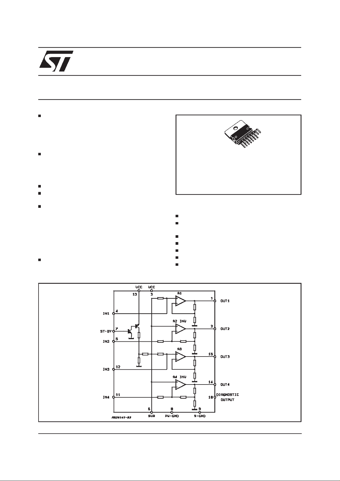
BLOCK DIAGRAM
October 1998
1/14
Page 2
TDA7375A
DESCRIPTION
The TDA7375A is a new technology class AB car
radio amplifier able to work either in DUAL
BRIDGEor QUADSINGLE ENDED configuration.
The exclusive fully complementarystructureof the
output stage and the internally fixed gain guaran-
tee the highest power performances with extremely reduced component count. The on board
clip detector simplifies gain compression operation. The fault diagnostic makes it possible to detect mistakes during car radio set assembly and
wiring in the car.
GENERALSTRUCTURE
ABSOLUTEMAXIMUM RATINGS
Symbol Parameter Value Unit
V
op
V
V
peak
I
O
I
O
P
tot
T
stg,Tj
Operating Supply Voltage 18 V
DC Supply Voltage 28 V
S
Peak Supply Voltage(for t = 50ms) 40 V
Output Peak Current (notrepitive t = 100µs) 4.5 A
Output Peak Current (repetitivef > 10Hz) 3.5 A
Power Dissipation T
Storage and Junction Temperature -40 to 150 °C
=85°C36W
case
THERMAL DATA
Symbol Description Value Unit
R
th j-case
Thermal Resistance Junction-case Max 1.8 °C/W
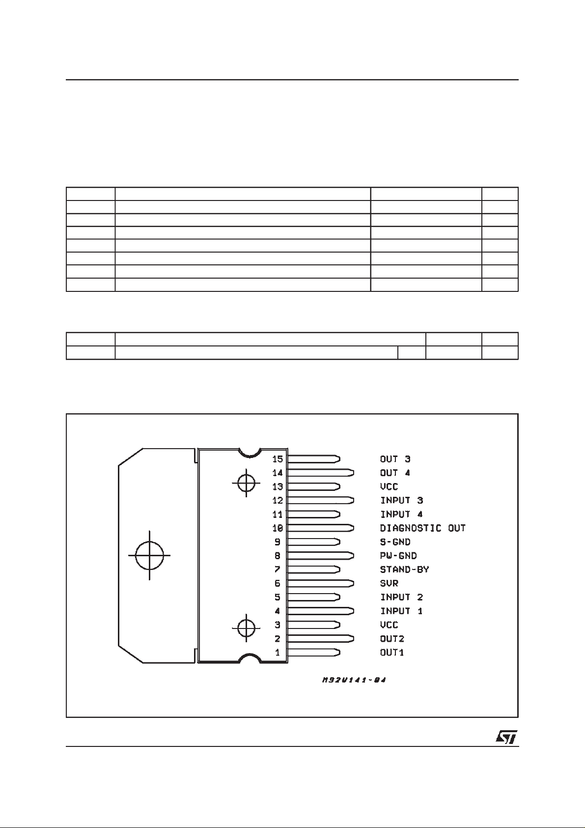
PIN CONNECTION (Topview)
2/14
Page 3

TDA7375A
ELECTRICALCHARACTERISTICS (Referto the testcircuit, VS=14.4V;RL=4Ω; f =1KHz;
T
=25°C,unless otherwise specified
amb
Symbol Parameter Test Condition Min. Typ. Max. Unit
V
S
I
d
V
OS
P
O
P
O max
P
O EIAJ
THD Distortion R
CT Cross Talk f = 1KHz Single Ended
R
IN
G
V
G
V
E
IN
SVR Supply Voltage Rejection R
A
SB
I
SB
V
SB
V
SB
I
pin7
I
cd off
I
cd on
V
sat pin10
(*) See built-in S/C protection description
(**) Pin 10 Pulled-up to 5V with 10KΩ;R
(***) Saturatedsquare waveoutput.
Supply Voltage Range 8 18 V
Total Quiescent DrainCurrent RL= ∞ 150 mA
Output Offset Voltage 150 mV
Output Power THD = 10%; RL=4
Bridge
Single Ended
Single Ended, R
Ω
23
6.5
=2
Ω
L
26
7
12
Max. Output Power (***) VS = 14.4V,Bridge 37 43 W
EIAJ Output Power (***) VS= 13.7V, Bridge 33 37 W
=4Ω
L
Single Ended, P
Bridge, P
O
= 0.1 to 4W
O
= 0.1 to10W
0.02
0.03 0.3
70
f = 10KHzSingle Ended
f = 1KHz Bridge
f = 10KHzBridge
Input Impedance Single Ended
Bridge
Voltage Gain Single Ended
Bridge
55
20
10
19
25
60
60
30
15
20
26
21
27
Voltage Gain Match 0.5 dB
Input Noise Voltage Rg= 0; ”A”weighted, S.E.
Non Inverting Channels
Inverting Channels
2
5
Bridge
Rg = 0;22Hz to 22KHz 3.5 µV
= 0; f = 300Hz 50 dB
g
Stand-by Attenuation PO=1W 80 90 dB
ST-BY Current Consumption V
= 0 to1.5V 100
ST-BY
ST-BY In ThresholdVoltage 1.5 V
ST-BY Out ThresholdVoltage 3.5 V
ST-BY Pin Current Play ModeV
Max Driving Current Under
=5V 50 µA
pin7
5mA
Fault (*)
Clipping Detector
d = 1%(**) 90
Output Average Current
Clipping Detector
d = 5%(**) 160 µA
Output Average Current
Voltage Saturation on pin10 Sink Currentat Pin 10= 1mA 0.7 V
=4Ω
L
W
W
W
%
%
dB
dB
dB
dB
K
KΩ
dB
dB
µV
µV
µ
µ
Ω
A
A
3/14
Page 4
TDA7375A
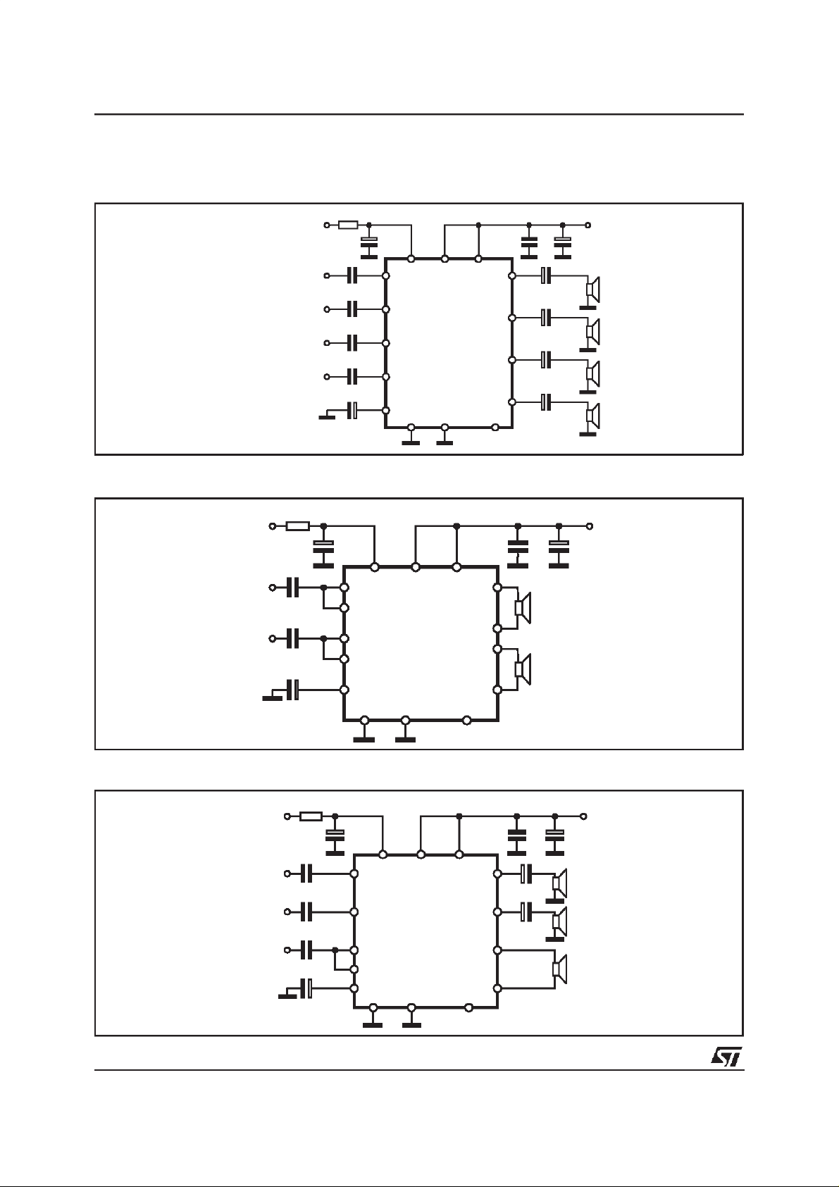
STANDARD TEST AND APPLICATION CIRCUIT
Figure 1: Quad Stereo
Note:
The output decoupling capaci t or s
(C9,C10,C11,C12)could bereducedto
1000µFifthe2Ωoperation is not
required.
Figure 2: Double Bridge
ST-BY
IN L
ST-BY
IN FR 5
IN RR 11
10K R1
IN FL
C1 0.22µF
C2 0.22µF
C4 0.22µF
C3 0.22µF
C8 47µF
10K R1
C5
10µF
C1 0.47µF
C2 0.47µF
C8 47µF
C7
10µF
7
13
4
12IN RL
6
89 10
3
DIAGNOSTICS
C4
100nF
13
7
4
3
1
5
12IN R
11
6
2
15
14
89 10
DIAGNOSTICS
C6
100nF
1
2
15
14
C10 2200µF
C9 2200µF
C11 2200µF
C12 2200µF
D94AU063A
OUT L
OUT R
D94AU064A
V
S
C5
1000µF
V
C3
1000µF
OUT FL
OUT FR
OUT RL
OUT RR
S
Figure 3: Stereo/Bridge
IN BRIDGE 12
4/14
ST-BY
IN L
IN L
10K
0.22µF
0.22µF
0.47µF
47µF
10µF
13
7
4
3
5
11
6
89 10
DIAGNOSTICS
15
14
1
2
2200µF
2200µF
D94AU065A
1000µF100nF
OUT L
OUT R
OUT
BRIDGE
V
S
Page 5
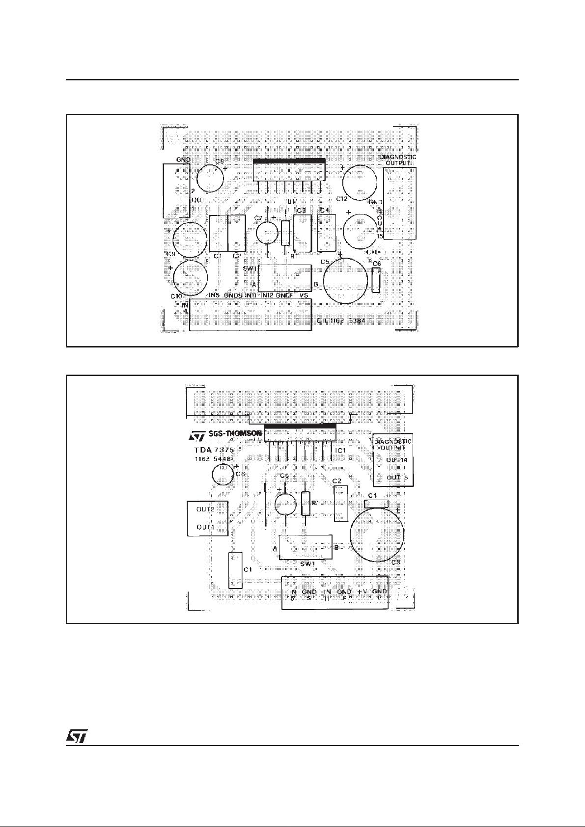
Figure 4: P.C. Board and ComponentLayout of the fig.1(1:1 scale).
TDA7375A
Figure 5: P.C. Board and ComponentLayout of the fig.2(1:1 scale).
5/14
Page 6

TDA7375A
Figure 6: QuiescentDrain Currentvs. Supply
Voltage(Single Ended and Bridge).
Figure 8: Output Power vs. Supply Voltage
Figure7: QuiescentOutputVoltage vs.Supply
Voltage (SingleEnded andBridge).
Figure9: OutputPower vs. Supply Voltage
Figure 10: OutputPowervs. SupplyVoltage
6/14
Figure11: Distortionvs. Output Power
Page 7

TDA7375A
Figure 12: Distortionvs. OutputPower
Figure 14: Cross-talkvs. Frequency
Figure13: Distortionvs. Output Power
Figure15: SupplyVoltage Rejection vs. Fre-
quency
Figure16:SupplyVoltageRejectionvs.Frequency
Figure17: Stand-byAttenuationvs. Threshold
Voltage
7/14
Page 8

TDA7375A
Figure 18: TotalPowerDissipationand Effi-
ciency vs. OutputPower
Figure19: TotalPower Dissipation and Effi-
ciencyvs. OutputPower.
8/14
Page 9

TDA7375A
High ApplicationFlexibility
The availability of 4 independentchannels makes
it possible to accomplish several kinds of applications ranging from 4 speakers stereo (F/R) to 2
speakersbridge solutions.
In case of working in single ended conditions the
polarity of the speakers driven by the inverting
amplifier must be reversedrespect to those driven
by noninverting channels.
This is to avoid phase inconveniences causing
sound alterations especially during the reproduction of low frequencies.
Easy SingleEnded to BridgeTransition
The change from single ended to bridge configurations is made simplyby means of a short circuit
across theinputs, that is no need of furtherexternal components.
Gain Internally Fixed to 20dB in Single Ended,
26dB inBridge
Advantagesof thisdesign choice are interms of:
componentsand space saving
output noise, supply voltage rejection and dis-
tortion optimization.
Silent Turn On/Off and Muting/Stand-by Function
The stand-by can be easily activated by means of
a CMOSlevel applied to pin 7 througha RC filter.
Under stand-by condition the device is turned off
completely (supply current = 1µA typ.; output at-
tenuation= 80dBmin.).
Every ON/OFFoperationis virtually pop free.
Furthemore, at turn-on the device staysin muting
condition for a time determined by the value assigned to theSVR capacitor.
While in muting the device outputs becomes insensitive to any kinds of signal that may be present at the input terminals. In other words every
transient coming from previous stages produces
no unplesantacousticeffectto the speakers.
Need of Bootstrap Capacitors.
The outputswing is limited only by theVCEsat
of the outputtransistors,which arein therange
of 0.3Ω (R
) each.
sat
Classical solutions adopting composite PNPNPN for the upper output stage have higher
saturationloss onthe topside of the waveform.
This unbalanced saturation causes a significant power reduction. The only way to recover
power consists of the addition of expensive
bootstrapcapacitors.
Absolute Stability Without Any External
Compensation.
Referring to the circuit of fig. 20 the gain
V
Out/VIn
R2/R1. The DC output (V
is greaterthan unity, approximately 1+
/2) is fixed by an
CC
auxiliaryamplifier common to allthe channels.
By controlling the amount of thislocal feedback
it is possibleto force the loop gain (A*β) toless
than unity at frequency for which the phase
shift is 180°. This means that the output buffer
is intrinsically stable and not prone to oscillation.
Most remarkably, the above feature has been
achieved in spite of the very low closed loop
gain of the amplifier.
In contrast, with the classical PNP-NPN stage,
the solution adopted for reducing the gain at
high frequencies makes use of external RC
networks,namely the Boucherotcells.
Figure20: TheNew OutputStage
OUTPUT STAGE
The fully complementary output stage was made
possible by the development of a new component: the ST exclusive power ICVPNP.
A noveldesign based uponthe connectionshown
in fig. 20 has then allowed the full exploitation of
its possibilities.
The clear advantagesthis new approachhas over
classicaloutput stages areas follows:
Rail-to-Rail Output Voltage Swing With No
BUILT–INSHORT CIRCUIT PROTECTION
Reliable and safe operation, in presence of all
kinds of short circuit involving the outputs is assured by BUILT-IN protectors. Additionally to the
AC/DC short circuit to GND, to V
, across the
S
speaker, a SOFT SHORT condition is signalled
out during the TURN-ON PHASE so assuring cor-
9/14
Page 10

TDA7375A
rect operation for the device itself and for the
loudspeaker.
This particular kind of protection acts in such a
way to avoid the device is turned on (by ST-BY)
when a resistive path (less than 16 ohms) is present between the output and GND. As the involved circuitry is normally disabled when a current higher than 5mA is flowing into the ST-BY
pin, it is important, in order not to disable it, to
have the external current source driving the STBY pin limited to 5mA.
This extrafunction becomes particularly attractive
when, in the single ended configuration, one capacitor is shared between two outputs (see fig.
21).
Figure 21.
Figure22: ClippingDetectionWaveforms
A current sinking at pin10 is provided when acertain distortionlevel is reachedat each output.This
function allows gain compression facility whenevertheamplifier is overdriven.
Supposing that the output capacitor C
out
for any
reason is shorted, the loudspeaker will not be
damaged beingthis soft short circuit conditionrevealed.
DiagnosticFacilities
The TDA7375 is equipped with a diagnostic circuitry able to detectthe followingevents:
Clippingin the output signal
Thermalshutdown
Outputfault:
– shortto GND
– shortto V
S
– softshort at turnon
The information is available across an open
collector output (pin 10) through a currentsinking whenthe event is detected
ThermalShutdown
In this case the output 10 will signal the proximity
of the junction temperature to the shutdown
threshold. Typically current sinking at pin 10 will
start ~10°C before the shutdown threshold is
reached.
HANDLING OF THE DIAGNOSTIC INFORMAFigure23: OutputFault Waveforms(see fig.24)
TDA7375A
10/14
Page 11

Figure 24: FaultWaveforms
ST-BY PIN
VOLTAGE
2V
OUTPUT
WAVEFORM
TDA7375A
t
OUT TO Vs SHORT
SOFT SHORT
t
OUT TO GND SHORT
Vpin 10
CHECK AT
(TEST PHASE)
CORRECT TURN-ON
TURN-ON
TION
As differentkinds of informationis available at the
same pin (clipping detection, outputfault, thermal
proximity),this signalmust be handledproperly in
order to discriminatethe event.
Figure 25: Waveforms
ST-BY PIN
VOLTAGE
Vs
OUTPUT
WAVEFORM
FAULT DETECTION
t
D94AU149A
SHORT TO GND
OR TO Vs
This could be done taking into account the different timing of the diagnostic output against different events.
Normally the clip detector signalling produces a
low levelat out 10 that is shorterreferred to every
t
10
Vpin
WAVEFORM
D94AU150
CLIPPING
SHORT TO GND
OR TO Vs
t
t
THERMAL
PROXIMITY
11/14
Page 12

TDA7375A
kind of fault detection; based on this assumption
an interface circuitry to differentiate the information is representedin the following schematic.
Figure 26.
TDA7375A
12/14
Page 13

TDA7375A
DIM.
MIN. TYP. MAX. MIN. TYP. MAX.
A5
B 2.65 0.104
C 1.6 0.063
D 1 0.039
E 0.49 0.55 0.019 0.022
F 0.66 0.75 0.026 0.030
G 1.02 1.27 1.52 0.040 0.050 0.060
G1 17.53 17.78 18.03 0.690 0.700 0.710
H1 19.6 0.772
H2 20.2 0.795
L 21.9 22.2 22.5 0.862 0.874 0.886
L1 21.7 22.1 22.5 0.854 0.870
L2 17.65 18.1 0.695 0.713
L3 17.25 17.5 17.75 0.679 0.689 0.699
L4 10.3 10.7 10.9 0.406 0.421 0.429
L7 2.65 2.9 0.104 0.114
M 4.25 4.55 4.85 0.167 0.179 0.191
M1 4.63 5.08 5.53 0.182 0.200 0.218
S 1.9 2.6 0.075 0.102
S1 1.9 2.6 0.075 0.102
Dia1 3.65 3.85 0.144 0.152
mm inch
0.197
0.886
OUTLINE AND
MECHANICAL DATA
Multiwatt15 V
13/14
Page 14

TDA7375A
Information furnished is believed tobe accurate and reliable. However, STMicroelectronics assumes no responsibility for the consequences
of use of such information nor for any infringement of patents or other rights of third parties which may result from its use. No license is
granted by implication or otherwise under any patent or patent rights of STMicroelectronics. Specification mentioned in this publication are
subject to change without notice. This publicationsupersedes and replaces all information previously supplied. STMicroelectronics products
are not authorized for use as critical components in life support devices or systems without express written approval of STMicroelectronics.
The ST logo is a registered trademark of STMicroelectronics
1998 STMicroelectronics – Printed in Italy – AllRightsReserved
MULTIWATTis aRegistered Trademark of the STMicroelectronics
STMicroelectronics GROUPOF COMPANIES
Australia - Brazil- Canada- China- France - Germany- Italy - Japan - Korea - Malaysia- Malta - Mexico - Morocco - The Netherlands-
Singapore - Spain- Sweden- Switzerland - Taiwan- Thailand - United Kingdom - U.S.A.
http://www.st.com
14/14
 Loading...