

Page 1

SERIAL BUS CONTROLLED AUDIO PROCESSOR
INPUTMULTIPLEXER:
- 4STEREOINPUTS
- ONEDIFFERENTIAL STEREO INPUT FOR
REMOTESOURCES
SELECTABLE INPUT GAIN FOR OPTIMAL
ADAPTIONTO DIFFERENTSOURCES
INPUT AND OUTPUT FOR EXTERNAL
EQUALIZER OR NOISE REDUCTION SYSTEM
VOLUMECONTROL IN 1.25dB STEPS
LOUDNESSFUNCTION
TREBLEAND BASS CONTROL
FOURSPEAKERATTENUATORS:
- 4 INDEPENDENTSPEAKERSCONTROL
IN 1.25dB STEPS FOR BALANCEAND
FADERFACILITIES
- INDEPENDENTMUTE FUNCTION
ALL FUNCTIONS PROGRAMMABLE VIA SERIAL BUS
SELECTABLE CHIP ADDRESS DEDICATED
PIN
TDA7310
PQFP44 (10 x 10)
ORDERING NUMBER: TDA7310
DESCRIPTION
The TDA7310 is a volume, tone (bass and treble)
and fader(front/r ear)processor for high qualityaudio
applicationsin car radioandHi-Fi systems.
Loudness and selectabl e input gain are provided.
The control of all fuctions is accomplished by serial
busmicroproc es sorinterface.
TheAC signalsettingis obtainedbyresis to rnetwork s
andswitchescombinedwith operationalamplifiers.
Thanks to the used BIP OLAR /CMOS Tecnology ,
LowDistortion,Low Noiseand DC steppingare obtained.
PIN CONNECTION (Top view)
November 1999
This is advanced information on a new product now in development or undergoing evaluation. Details are subject to change without notice.
1/15
Page 2

TDA7310
TEST CIRCUIT
THERMAL DATA
Symbol Description Value Unit
R
thj-pins
Thermal Resistance Junction-pins max 85 °C/W
ABSOLUTE MAXIMUM RATINGS
Symbol Parameter Value Unit
V
T
amb
T
stg
Operating Supply Voltage 10.2 V
S
Ambient Temperature -40 to 85
Storage Temperature Range -55 to +150 °C
QUICK REFERENCE DATA
Symbol Parameter Min. Typ. Max. Unit
V
V
CL
THD Total Harmonic Distortion V = 1Vrms f = 1KHz 0.01 %
S/N Signal to Noise Ratio 106 dB
S
Supply Voltage 6 9 10 V
S
Max. input signal handling 2 Vrms
Channel Separation f = 1KHz 103 dB
C
Volume Control 1.25dB step -78.75 0 dB
Bass and Treble Control 2dB step -14 +14 dB
Fader and Balance Control 1.25dB step -38.75 0 dB
Input Gain 6.25dB step 0 18.75 dB
Mute Attenuation 100 dB
C
°
2/15
Page 3
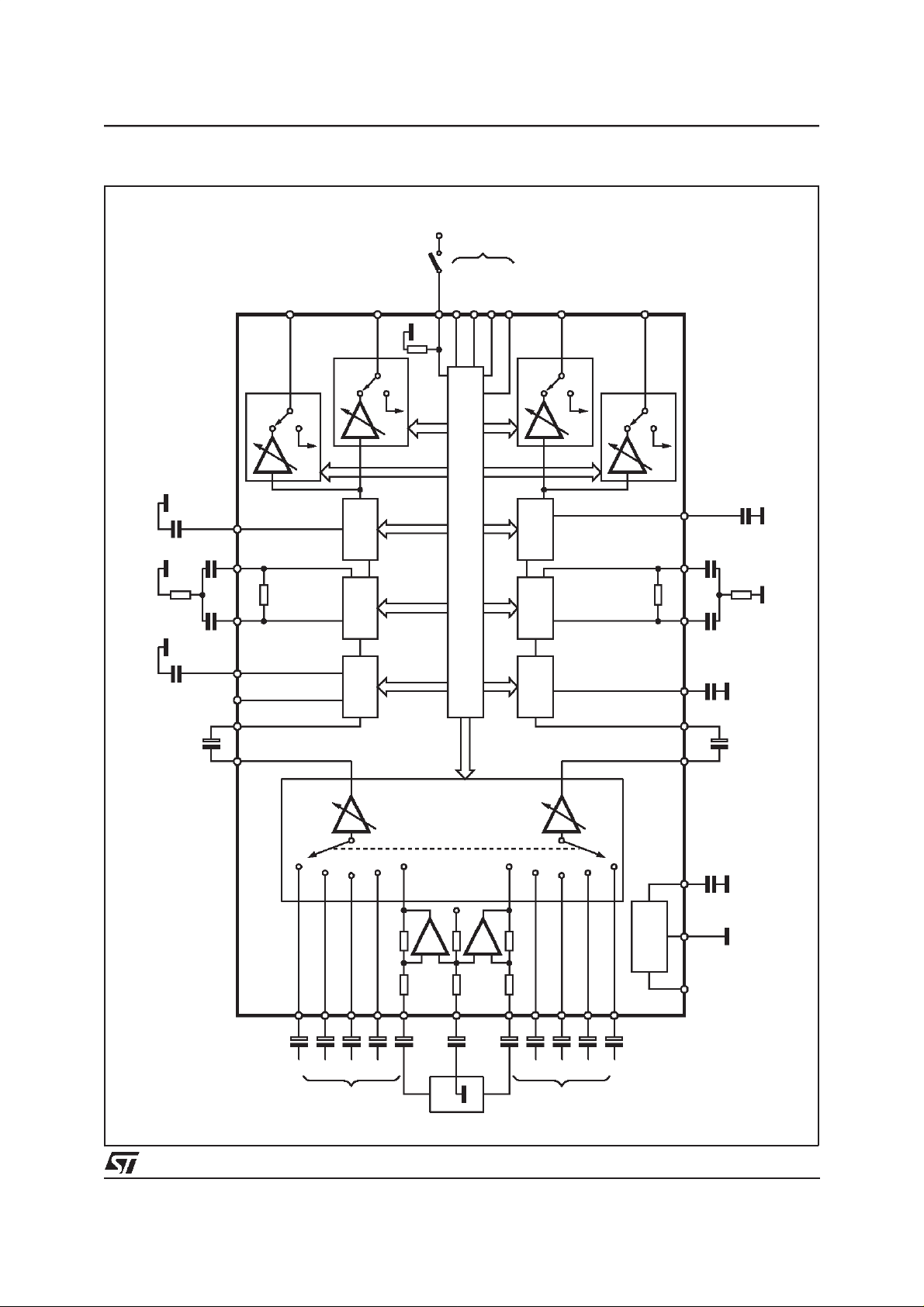
BLOCK DIAGRAM
+V
TDA7310
CC
BUS
C22
5.6K R2
C16
2.7nF
C20
C19
100nF
TREBLE(L)
BIN(L)
100nF
BOUT(L)
100nF
LOUD(L)
LOUD SW
10
31
32
38 39
ATT
SPKR
OUT
2
RB
LEFT FRONT
MUTE
ATT
SPKR
VOL
OUT
LEFT REAR
42
TREBLE
BASS
+ LOUD
MUTE
50K
ADDR
37
SCL
SEN
654
SERIAL BUS DECODER + LATCHES
SDA
3
DIGGND
SPKR
BASS TREBLE
VOL
ATT
+ LOUD
OUT
43
RIGHT FRONT
MUTE
ATT
SPKR
OUT
41
RIGHT REAR
RB
MUTE
13
36 35
D94AU170
TREBLE(R)
BOUT(R) BIN(R)
C17 C18
100nF 100nF 100nF
LOUD(R)
C15
C21
5.6K R1
2.7nF
OUT(R) IN(R)
22µFC12
AGND CREF
CC
V
C13 2.2µF
C14 2.2µF
OUT(L) IN(L)
30 29
4x
2.2µF
L1 28L1L2 27L2L3 26L3L4 25
C1
C2
C3
LEFT
INPUTS
C4
INPUT
+ GAIN
SELECTOR
L5
L4
16
C5
17
SGND
4.7µF
C6
L5
CD
R5
18
R4 19R4R3 20R3R2 21
10µF
4.7µF
C7
C8
R5
C9
RIGHT
INPUTS
R2
C10
24 R1
R1
C11
15 14 40
SUPPLY
897
4x
2.2µF
3/15
Page 4

TDA7310
ELECTRICALCHARACTERISTICS (T
=25°C, VS= 9V, RL= 10KΩ,RG= 600Ω,GV=0dB, f = 1KHz
amb
unless otherwise specified) (referto the test circuit)
Symbol Parameter Test Condition Min. Typ. Max. Unit
SUPPLY
V
S
I
S
SVR Ripple Rejection 60 85 dB
Supply Voltage 6 9 10 V
Supply Current 4 8 11 mA
INPUT SELECTORS
R
II
V
CL
CMRR Common Mode Rejection
INS Input Separation (2) 80 100 dB
R
L
G
INmin
G
INmax
G
STEP
e
IN
V
DC
Input Resistance Input 1, 2, 3, 4 50 K
Differential Input 10 KΩ
Clipping Level 2 2.5 Vrms
65 dB
Differential Input
Output Load resistance 2 KΩ
Min. Input Gain -1 0 1 dB
Max. Input Gain 18.75 dB
Step Resolution 6.25 dB
Input Noise G = 18.75dB 2
DC Steps adjacent gain steps 4 mV
G = 18.75 to Mute 4 mV
VOLUMECONTROL
Ω
V
µ
R
IN
C
RANGE
A
VMIN
A
VMAX
A
STEP
E
A
E
T
V
DC
Input Resistance 33 kΩ
Control Range 75 dB
Min. Attenuation -1 0 1 dB
Max. Attenuation 75 dB
Step Resolution 1.25 dB
Attenuation Set Error AV= 0 to -20dB
Tracking Error 2dB
DC Steps adjacent attenuation steps
SPEAKERATTENUATORS
Control Range 37.5 dB
Step Resolution 1.25 dB
Attenuation set error 1.5 dB
Output Mute Attenuation 80 100 dB
DC Steps adjacent att. steps
BASS CONTROL(1)
Control Range +14 dB
Step Resolution 2 dB
R
B
V
DC
Internal Feedback Resistance 50 KΩ
DC Steps adjacent control steps 0.1 mV
A
= -20 to -60dB
V
From 0dB to A
from 0 to mute
Vmax
-1.25
-3
0 1.25
0.1
0.5
0
1
2
dB
mV
mV
mV
mV
dB
4/15
Page 5
TDA7310
ELECTRICALCHARACTERISTICS (continued)
Symbol Parameter Test Condition Min. Typ. Max. Unit
TREBLECONTROL(1)
Control Range +14 dB
Step Resolution 2 dB
V
DC
AUDIO OUTPUTS
GENERAL
DC Steps adjacent control steps 0.1 mV
Clipping Level d = 0.3% 2.5 Vrms
Output Load Resistance 2 K
Output Load Capacitance 10 nF
Output resistance 75 120 Ω
DC Voltage Level 4.2 4.5 4.8 V
Ω
e
NO
S/N Signal to Noise Ratio all gains = 0dB; V
d Distortion V
Output Noise BW = 20-20KHz, flat
output muted
all gains = 0dB
O
= 1Vrms 0.01 %
IN
2.5
515
µV
µV
= 1Vrms 106 dB
Sc Channel Separation left/right 80 103 dB
Total Tracking error A
= 0 to -20dB
V
-20 to -60 dB
0
0
1
2
dB
dB
BUS INPUTS
V
IL
V
IH
V
O
Input Low Voltage 1V
Input High Voltage 3 V
Output Voltage SDA
IO= 1.6mA 0.4 V
Acknowledge
LOUDNESSSWITCH
V
IL
V
IH
I
IN
Input Low Voltage 1V
Input High Voltage 3 V
Input Current -5 +5 µA
DC Step ON
OFF position 0.1 mV
←→
Loudness OFF = pin38 Open; LoudnessON = pin 38Closed to GND
ADDRESSPIN (Internal 50KΩpulldown resistor)
V
IL
V
IH
I
IN
Notes:
(1) Bass and Trebleresponse see attached diagram(fig.17). The center frequency and quality of the resonance behaviour can be choosen by
the external circuitry. A standard first order bass response can be realized by a standard feedback network
(2) The selected input is groundedthru the 2.2µF capacitor.
Input Low Voltage 1V
Input High Voltage VCC-1V V
Input Current µA
5/15
Page 6

TDA7310
APPLICATIONSUGGESTION(see to Test circuit)
Component Recc. Value Purpose Smallerthan Recc. Value Larger than
C1 to C4,
C8 to C11
C5, C7
C6
C12 22µFC
C13, C14 2.2µF Decoupling Input-Output
C15, C16 100nF Loudness characteristic
C17, C18
R1
C!9, C20
R2
C21
C22
2.2µF THD optimization at low
4.7µF
10µF
100nF
5.6kΩ
100nF
5.6kΩ
2.7nF Treble Filter Higher cut frequency Lower cut frequency
frequencies
CMRR optimization
differential input
• SVR optimization
REF
< -66 dB
if external equalizer is
not used
Bass Filter
(standard T - type)
cut freq. = 100Hz
Worse THD at very low
frequencies
Worse CMRR for ratio not equal to
Better SVR at low
frequencies
Worse SVR at low
frequencies
1
⁄
2
Figure 1: Loudnessversus Volume Attenuation
Figure2: Loudnessversus Frequency
(C
LOUD
= 100nF)
6/15
Page 7

TDA7310
Figure 3: Loudnessversus External Capacitors
LOUDNESS
V
=9V
S
Volume= -40dB
All other control flat
= 2.2µF
C
in
Figure4: Noisevs. Volume/GainSettings
Figure 5: Signalto Noise Ratio vs. Volume
Setting
Figure6: Distortionvs. Load Resistance
7/15
Page 8

TDA7310
Figure 7 : ChannelSeparation(L→R)vs.
Frequency
Figure 9 : SupplyVoltage Rejection vs.
Frequency
Figure8 : Input Separation(L1→L2, L3, L4) vs.
Frequency
Figure10: OutputClipping Level vs. Supply
Voltage
8/15
Page 9

TDA7310
Figure 11: QuiescentCurrent vs. Supply Voltage
Figure 13: Bass Resistancevs. Temperature
Figure12: SupplyCurrent vs. Temperature
Figure14: TypicalTone Response (with the ext.
components indicated in the test
circuit)
9/15
Page 10

TDA7310
APPLICATIONINFORMATION(continued)
SERIALBUS INTERFACE
S-BUS Interface and I
2
CBUSCompability
Data transmission from microprocessor to the
TDA7310 and viceversa takes place thru the 3wire S-BUS interface, consisting of the three lines
SDA, SCL, SEN. If SDA and SEN inputs are
short-circuited together, then the TDA7310 appears as a standardI
According to I
2
CBUS slave.
2
CBUS specification the S-BUS
lines are connected to a positive supply voltage
via pull-up resistors.
Data Validity
As shown in fig. 15, the data on the SDA line
must be stable during the high period of the clock.
The HIGH and LOW state of the data line can
only change when the clock signal on the SCL
line is LOW.
Start and Stop Conditions
2
CBUS:
I
as shown in fig. 16 a start condition is a HIGH to
LOW transition of the SDA line while SCL is
HIGH. The stop condition is a LOW to HIGH transition of the SDA line while SCL is HIGH.
S-bus:
the start/stop conditions (points 1 and 6) are de-
tected exclusively by a transition of the SEN line
(1→0/0→1)wile the SCL line is at the HIGH
level.
The SDA line is only allowed to change during the
time the SCL line is low (points 2, 3, 4, 5). after
the start information(point 1) the SEN line returns
to the HIGH level and remains uncharged for all
the time the transmission is performed.
Figure15: DataValidity on the I2CBUS
Figure16: TimingDiagramof S-BUSand I
2
CBUS
Byte Fornat
Every byte transferred on the SDA line must contain 8 bits. Each byte must be followed by an acknowledgebit. The MSB is transferredfirst.
Acknowledge
The master (µP) puts a resistiveHIGH level on
2
Figure 17: Acknowledgeon the I
10/15
CBUS
the SDA line during the acknowledge clock pulse
(see fig. 17). The peripheral(audioprocessor)that
acknowledges has to pull-down (LOW) the SDA
line during the acknowledge clock pulse, so that
the SDA line is stable LOW duringthis clock.
Page 11

TDA7310
APPLICATIONINFORMATION(continued)
The audioprocessor which has been addressed
This approach of course is less protected from
misworkingand decreasesthe noise immunity.
has to generate an acknowledge after the reception of eachbyte, otherwise the SDA line remains
at the HIGH level during the ninth clock pulse
time. In this case the master transmitter can generate the STOP information in order to abort the
transfer.
InterfaceProtocol
The interface protocol comprises:
A startcondition (s)
A chip address byte, containing the TDA7310
address(the 8th bit of the bytemust be 0). The
Transmissionwithout Acknowledge
Avoiding to detect the acknowledge of the audioprocessor, the µP can use a simpler transmission:
simply it waits one clock without checking the
TDA7310must always acknowledgeat the end
of each transmittedbyte.
A sequenceof data (N-bytes + acknowledge)
A stopcondition (P)
slave acknowledging,and sends the new data.
TDA7310 ADDRESS
MSB first byte LSB MSB LSB MSB LSB
S100010A0
ACK = Acknowledge
S = Start
P = Stop
MAX CLOCK SPEED 100kbits/s
ACK DATA ACK DATA ACK P
Data Transferred (N-bytes + Acknowledge)
SOFTWARESPECIFICATION
Chip address
1
MSB
A = LOGIC LEVEL ON PIN ADDR
00010A0
LSB
DATA BYTES
MSB LSB FUNCTION
0
1
1
1
1
0
0
0
Ax = 1.25dB steps; Bx = 10dB steps; Cx = 2dB steps; Gx = 6.25dB steps
0
1
1
0
0
1
1
1
B2
0
1
0
1
0
1
1
B1
B1
B1
B1
B1
G1
0
1
B0
B0
B0
B0
B0
G0
C3
C3
A2
A2
A2
A2
A2
S2
C2
C2
A1
A1
A1
A1
A1
S1
C1
C1
A0
A0
A0
A0
A0
S0
C0
C0
Volume control
Speaker ATT LR
Speaker ATT RR
Speaker ATT LF
Speaker ATT RF
Audio switch
Bass control
Treble control
STATUSAFTER POWER ON RESET
Volume
speaker
audio Switch
bass
treble
gain
-77.5dB
-37.5dB
Stereo 5
+2dB
+2dB
0dB
11/15
Page 12

TDA7310
SOFTWARESPECIFICATION(continued)
DATA BYTES (detailed description)
Volume
MSB LSB FUNCTION
0 0 B2 B1 B0 A2 A1 A0 Volume 1.25dB steps
0
0
0
0
1
1
1
1
0 0 B2 B1 B0 A2 A1 A0 Volume 10dB steps
0
0
0
0
1
1
1
1
0
0
1
1
0
0
1
1
0
1
0
1
0
1
0
1
0
0
1
1
0
0
1
1
For example a volumeof -45dB is given by:
00100100
0
1
0
1
0
1
0
1
0
-1.25
-2.5
-3.75
-5
-6.25
-7.5
-8.75
0
-10
-20
-30
-40
-50
-60
-70
Speaker Attenuators
MSB LSB FUNCTION
1
1
1
1
0
0
1
1
0
1
0
1
B1
B1
B1
B1
0
0
1
1
11111 Mute
B0
B0
B0
B0
0
1
0
1
A2
A2
A2
A2
0
0
0
0
1
1
1
1
A1
A1
A1
A1
0
0
1
1
0
0
1
1
A0
A0
A0
A0
0
1
0
1
0
1
0
1
Speaker LF
Speaker RF
Speaker LR
Speaker RR
For example attenuationof 25dB on speaker RF is given by:
10110100
0
-1.25
-2.5
-3.75
-5
-6.25
-7.5
-8.75
0
-10
-20
-30
12/15
Page 13

Audio Switch
MSB LSB FUNCTION
0 1 0 G1 G0 S2 S1 S0 Audio Switch
0
0
0
0
1
1
1
1
0
0
1
1
0
1
0
1
0
0
1
1
0
0
1
1
0
1
0
1
0
1
0
1
Stereo 1
Stereo 2
Stereo 3
Stereo 4
Stereo 5
Not allowed
Not allowed
Not allowed
+18.75dB
+12.5dB
+6.25dB
0dB
For example to selectthe stereo 2 input with a gainof +12.5dB the 8bit stringis:
01001001
Bass andTreble
TDA7310
0
0
1
1
1
1
0
1
C3
C3
0
0
0
0
0
0
0
0
1
1
1
1
1
1
1
1
C2
C2
0
0
0
0
1
1
1
1
1
1
1
1
0
0
0
0
C3 = Sign
For example Bass at -10dBis obtainedby the following8 bitstring:
01100010
C1
C1
0
0
1
1
0
0
1
1
1
1
0
0
1
1
0
0
C0
C0
Bass
Treble
0
1
0
1
0
1
0
1
1
0
1
0
1
0
1
0
-14
-12
-10
-8
-6
-4
-2
0
0
2
4
6
8
10
12
14
2
Purchase of I
Rights to use these components in an I
C Componentsfrom STMicroelectronics,conveys a license under the Philips I2C Patent
2
C system, provided that the system conforms to the I2C
Standard Specificationsas definedby Philips.
13/15
Page 14

TDA7310
DIM.
mm inch
MIN. TYP. MAX. MIN. TYP. MAX.
A 2.45 0.096
A1 0.25
0.010
A2 1.95 2.00 2.10 0.077 0.079 0.083
B 0.30 0.45 0.012 0.018
c 0.13 0.23 0.005 0.009
D 12.95 13.20 13.45 0.51 0.52 0.53
D1 9.90 10.00 10.10 0.390 0.394 0.398
D3 8.00 0.315
e 0.80 0.031
E 12.95 13.20 13.45 0.510 0.520 0.530
E1 9.90 10.00 10.10 0.390 0.394 0.398
E3 8.00 0.315
L 0.65 0.80 0.95 0.026 0.031 0.037
L1 1.60 0.063
K0°(min.),7°(max.)
OUTLINE AND
MECHANICAL DATA
PQFP44 (10 x 10)
D
D1
A1
33
34
B
44
1
e
23
11
PQFP44
22
L1
E
L
E3D3E1
12
0.10mm
.004
Seating Plane
B
K
A
A2
C
14/15
Page 15

TDA7310
Information furnished is believed to be accurate and reliable. However, STMicroelectronics assumes no responsibility for the consequences
of use of such information nor for any infringement of patents or other rights of third parties which may result from its use. No license is
granted by implication or otherwise under any patent or patent rights of STMicroelectronics. Specification mentioned in this publication are
subject to change without notice. This publication supersedes and replaces all information previously supplied. STMicroelectronics products
are not authorized for use as critical components in life support devices or systems without express written approval of STMicroelectronics.
The ST logo is a registered trademark of STMicroelectronics
1999STMicroelectronics – Printed in Italy– All Rights Reserved
STMicroelectronics GROUP OF COMPANIES
Australia - Brazil - China - Finland - France - Germany - Hong Kong - India - Italy - Japan - Malaysia - Malta - Morocco -
Singapore - Spain - Sweden - Switzerland - United Kingdom - U.S.A.
http://www.st.com
15/15
 Loading...