

Page 1
TDA7297
15+15W DUAL BRIDGE AMPLIFIER
WIDESUPPLYVOLTAGERANGE(6V -18V)
MINIMUMEXTERNALCOMPONENTS
– NOSWR CAPACITOR
– NOBOOTSTRAP
– NOBOUCHEROTCELLS
– INTERNALLYFIXEDGAIN
STAND-BY & MUTEFUNCTIONS
SHORTCIRCUITPROTECTION
THERMALOVERLOADPROTECTION
DESCRIPTION
The TDA7297 is a dual bridge amplifier specially
designed for TV and PortableRadio applications.
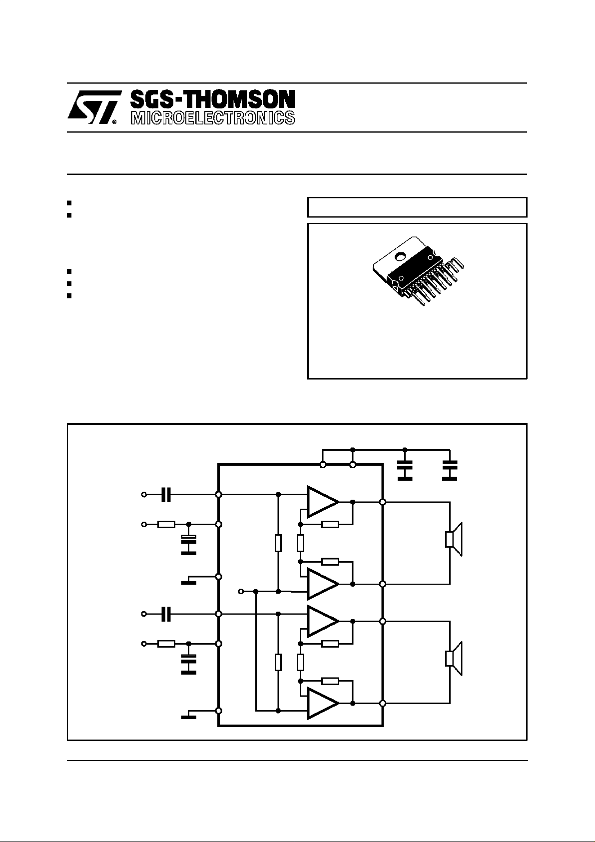
BLOCK AND APPLICATION DIAGRAM
0.22µF
IN1
ST-BY 7
4
TECHNOLOGYBI20II
Multiwatt 15
ORDERING NUMBER: TDA7297
V
CC
133
+
-
1
470µF 100nF
OUT1+
May 1997
S-GND
0.22µF
IN2
MUTE 6
PW-GND
9
12
8
Vref
15
14
2
OUT1-
OUT2+
OUT2-
D94AU175B
1/9
-
+
+
-
-
+
Page 2
TDA7297
ABSOLUTE MAXIMUM RATINGS
Symbol Parameter Value Unit
V
I
P
T
T
stg,Tj
THERMAL DATA
Symbol Description Value Unit
R
th j-case
Supply Voltage 20 V
S
Output Peak Current (internally limited) 2 A
O
Total Power Dissipation (T
tot
Operating Temperature 0 to 70
op
=70°C) 33 W
case
Storage and Junction Temperature -40 to +150 °C
Thermal Resistance Junction to case Typ. 1.4 Max. 2
°
C/W
°
C
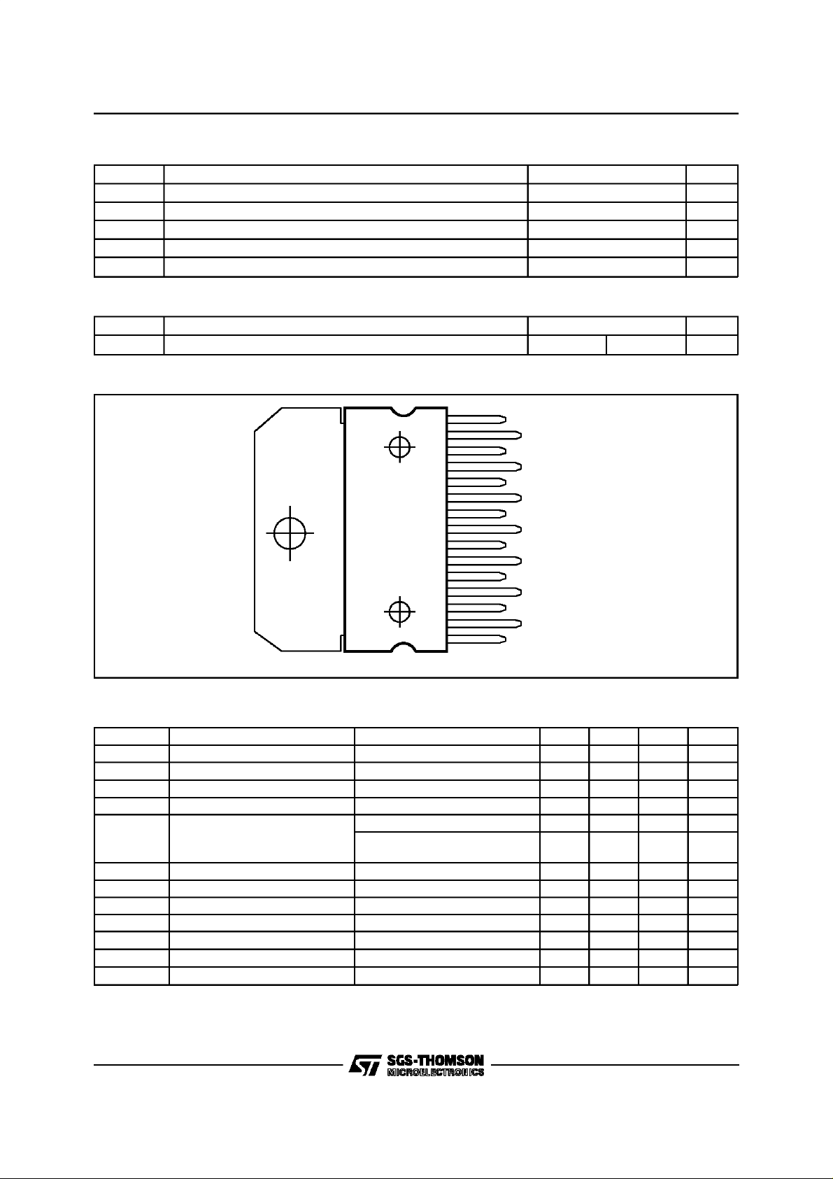
PIN CONNECTION
ELECTRICAL CHARACTERISTICS (VCC= 16.5V, RL=8Ω, f = 1kHz, T
(Top view)
15
14
13
12
11
10
9
8
7
6
5
4
3
2
1
D95AU261
OUT2+
OUT2VCC
IN2
N.C.
N.C.
S-GND
PW-GND
ST-BY
MUTE
N.C.
IN1
V
CC
OUT1OUT1+
amb
=25°C unless otherwise
specified.)
Symbol Parameter Test Condition Min. Typ. Max. Unit
V
CC
I
q
V
OS
P
O
THD Total Harmonic Distortion P
SVR Supply Voltage Rejection f = 100Hz V
CT Crosstalk 46 60 dB
A
MUTE
T
W
G
V
∆Gv Voltage Gain Matching 0.5 dB
R
Supply Range 6.5 18 V
Total Quiescent Current RL= ∞ 50 65 mA
Output Offset Voltage 120 mV
Output Power THD = 10% 13 15 W
= 1W 0.1 0.3 %
O
P
= 0.1W to 5W
O
f = 100Hz to 15kHz
= 0.5V 40 56 dB
R
Mute Attenuation 60 80 dB
Thermal Threshold 150 °C
Closed Loop Voltage Gain 31 32 33 dB
Input Resistance 25 30 K
i
1%
Ω
2/9
Page 3
TDA7297
ELECTRICALCHARACTERISTICS
Symbol Parameter Test Condition Min. Typ. Max. Unit
VT
VT
MUTE
ST-BY
I
ST-BY
e
N
Mute Threshold VO= -30dB 2.3 2.9 4.1 V
St-by Threshold 0.8 1.3 1.8 V
ST-BY current V6 = GND 100
Total Output Noise Voltage A curve
APPLICATIONSUGGESTION
STAND-BYAND MUTE FUNCTIONS
(A) MicroprocessorApplication
In order to avoid annoying ”Pop-Noise” during
Turn-On/Off transients, it is necessary to guarantee the right St-by and mute signals sequence.
It is quite simple to obtain this functionusing a microprocessor(Fig.1 and 2).
At first St-by signal (from mP) goes high and the
voltage across the St-by terminal (Pin 7) starts to
increase exponentially. The external RC network
is intended to turn-on slowly the biasing circuits of
(Continued)
f = 20Hz to 20kHz
150
220 500
the amplifier, this to avoid ”POP” and ”CLICK” on
the outputs.
When this voltage reaches the St-by threshold
level, the amplifier is switched-onand the external
capacitors in series to the input terminals (C3,
C5) start to charge.
It’s necessaryto mantain the mute signal low until
the capacitors are fully charged, this to avoid that
the device goes in play mode causing a loud ”Pop
Noise”on the speakers.
A delay of 100-200ms between St-by and mute
signals is suitable for a properoperation.
Figure 1: MicroprocessorApplication
V
CC
µ
µ
µV
A
V
µP
IN1
ST-BY
IN2
MUTE
C1 0.22µF
R1 10K
C2
10µF
C3 0.22µF
R2 10K
C4
1µF
PW-GND
S-GND
4
7
9
12
6
8
Vref
133
15
14
1
OUT1+
2
OUT1-
OUT2+
OUT2-
+
-
-
+
+
-
-
+
C5
470µF
D95AU258A
C6
100nF
3/9
Page 4

TDA7297
Figure 2:
MicroprocessorDriving Signals.
+VS(V)
+18
V
IN
(mV)
V
ST-BY
pin 7
1.8
1.3
0.8
V
MUTE
pin 6
4.1
2.9
2.3
I
q
(mA)
V
OUT
(V)
OFF
ST-BY
MUTE
PLAY MUTE ST-BY
(B) Low Cost Application
In low cost applications where the mP is not present, the suggestedcircuit is shown in fig.3.
The St-by and mute terminals are tied together
and they are connected to the supply line via an
OFF
D96AU259
externalvoltage divider.
The device is switched-on/off from the supply line
and the external capacitor C4 is intended to delay
the St-by and mute threshold exceeding, avoiding
”Popping”problems.
4/9
Page 5

TDA7297
Figure 3:
Stand-aloneLow-costApplication.
IN1
R1
47K
R2
47K
C4
10µF
C3 0.22µF
IN1
ST-BY
S-GND
C5 0.22µF
IN2
MUTE
4
7
9
12
6
Vref
V
CC
133
+
-
-
+
+
-
1
2
15
C1
470µF
OUT1+
OUT1-
OUT2+
C2
100nF
Figure 3b:
PW-GND
-
8
+
14
PCB and ComponentLayout of the Application Circuit (Fig. 1).
OUT2-
D95AU260
5/9
Page 6

TDA7297
Figure 4:
THD(%)
10
0.1
0.010
Figure 6:
THD(%)
10
1
0.1
0.010
100 1k 10k 20k
Distortionvs OutputPower
Vcc = 16.5V
1
0.1 1 10 20
Rl = 8 ohm
f = 15K Hz
f=5KHz
f=1KHz
Pout (W)
Distortionvs Frequency
Vcc = 16.5V
Rl = 8 ohm
Pout = 100mW
Pout = 5W
freq ue n c y (Hz)
Figure5:
THD(%)
10
1
0.1
0.010
Figure7:
Leve l(dBr)
5.0000
4.0000
3.0000
2.0000
1.0000
0.0
-1.000
-2.000
-3.000
-4.000
-5.000
Distortionvs Output Power
Vcc = 12 V
Rl = 8 ohm
f=15KHz
f=5KHz
f=1KHz
0.1 1 10
Pout (W)
FrequencyRespone
Vcc = 16.5V
Rl = 8 ohm
Pou t = 1W
10 100 1k 10k 100 k
frequency(Hz)
Figure 8: OutputPower vs Supply Voltage
)
Po(W
20.000
18.000
16.000
14.000
12.000
10.000
8.00 00
6.00 00
4.00 00
2.00 00
0.0
6.000 7.000 8.000 9.0 00 10. 00 11.00 12. 00 13.00 14. 00 15 . 00 16. 00 17. 00 18.00
6/9
Rl = 8 ohm
f = 1KHz
d=10%
d=1%
Vs(V)
Figure9: Total Power Dissipation& Efficiencyvs
OutputPower
Ptot(W)
16
14
12
Ptot
µ
10
8
6
4
Vcc=16.5V
Rl= 8ohm(bothchannels)
f=1KHz
2
0
012345678910111213141516
2XPout(W)
µ(%)
80
75
70
65
60
55
50
45
40
35
30
25
20
15
10
5
0
Page 7

TDA7297
Figure 10:
Attenuation (dB)
10
0
-10
-20
-30
-40
-50
-60
-70
-80
-90
-100
1 1.5 2 2.5 3 3.5 4 4.5 5
MuteAttenuationvs. V pin.6
Vpin.6(V)
Figure 12:
QuiscentCurrent vs. SupplyVoltage
Iq(mA)
70
65
60
55
50
45
40
35
30
6789101112131415161718
Vsupply(V)
Figure11:
Attenuation (dB)
10
0
-10
-20
-30
-40
-50
-60
-70
-80
-90
-100
-110
-120
0 0.2 0.4 0.6 0.8 1 1.2 1.4 1.6 1.8 2 2.2 2.4
Stand-ByAttenuation vs Vpin.7
Vpin.7(V)
7/9
Page 8

TDA7297
MULTIWATT15 PACKAGE MECHANICAL DATA
DIM.
A 5 0.197
B 2.65 0.104
C 1.6 0.063
D 1 0.039
E 0.49 0.55 0.019 0.022
F 0.66 0.75 0.026 0.030
G 1.02 1.27 1.52 0.040 0.050 0.060
G1 17.53 17.78 18.03 0.690 0.700 0.710
H1 19.6 0.772
H2 20.2 0.795
L 21.9 22.2 22.5 0.862 0.874 0.886
L1 21.7 22.1 22.5 0.854 0.870 0.886
L2 17.65 18.1 0.695 0.713
L3 17.25 17.5 17.75 0.679 0.689 0.699
L4 10.3 10.7 10.9 0.406 0.421 0.429
L7 2.65 2.9 0.104 0.114
M 4.25 4.55 4.85 0.167 0.179 0.191
M1 4.63 5.08 5.53 0.182 0.200 0.218
S 1.9 2.6 0.075 0.102
S1 1.9 2.6 0.075 0.102
Dia1 3.65 3.85 0.144 0.152
MIN. TYP. MAX. MIN. TYP. MAX.
mm inch
8/9
Page 9

TDA7297
Information furnished is believed to be accurate and reliable. However, SGS-THOMSON Microelectronics assumes no responsibility for the
consequences of use of such information nor for any infringement of patents or other rights of third parties which may result from its use. No
license is granted by implication or otherwise under any patent or patent rights of SGS-THOMSON Microelectronics. Specification mentioned
in this publication are subject to change without notice. This publication supersedes and replaces all information previously supplied.
SGS-THOMSON Microelectronics products arenotauthorized for useas criticalcomponents in life support devices or systems without express
written approval of SGS-THOMSON Microelectronics.
1997 SGS-THOMSON Microelectronics – Printed in Italy – AllRights Reserved
SGS-THOMSON Microelectronics GROUP OF COMPANIES
Australia - Brazil - Canada - China - France - Germany - Hong Kong - Italy - Japan - Korea - Malaysia - Malta - Morocco - The Netherlands-
Singapore - Spain - Sweden - Switzerland- Taiwan - Thailand - United Kingdom - U.S.A.
9/9
 Loading...