

Page 1
12 +12W STEREO AMPLIFIERWITH MUTING
WIDESUPPLYVOLTAGERANGE
HIGHOUTPUTPOWER
12+12W@ V
MUTE FACILITY (POP FREE) WITH LOW
CONSUMPTION
AC SHORT CIRCUIT PROTECTION
THERMAL OVERLOADPROTECTION
=28V, RL=8Ω, THD=10%
S
TDA7263M
DESCRIPTION
The TDA7263M is class AB dual audiopoweramplifier assembled in the Multiwatt package, specially designed for high quality sound application
as HI-FI music centers and stereo TV sets.
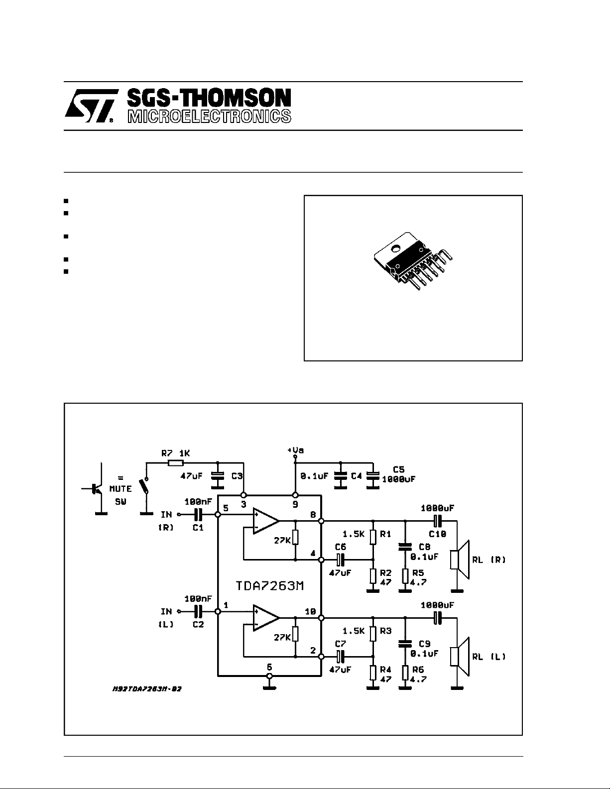
APPLICATIONCIRCUIT
Multiwatt11
ORDERING NUMBER:TDA7263M
March 1995
1/7
Page 2
TDA7263M
ABSOLUTE MAXIMUMRATINGS
Symbol Parameter Value Unit
V
S
I
O
I
O
P
tot
T
op
T
stg,Tj
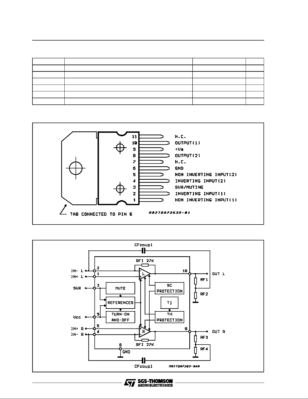
PIN CONNECTION (Top view)
SupplyVoltage 35 V
Output Peak Current (repetitive f >20Hz) 2.5 A
Output Peak Current (non repetitive, t = 100µs) 3.5 A
TotalPower Dissipation (T
=70°C) 30 W
case
Operating Temperature Range 0 to 70 °C
Storage & Junction Temperature -40 to 150 °C
Figure1: Block Diagram
2/7
Page 3

TDA7263M
THERMAL DATA
Symbol Parameter Value Unit
R
th j-case
Thermal resistance junction to case Max 2.5 °C/W
ELECTRICAL CHARACTERISTICS (Refer to the stereo test and applicationcircuit, VS= 28V;RL=8
Gv= 30dB;f = 1KHz;T
Symbol Parameter Test Condition Min. Typ. Max. Unit
V
S
V
O
I
q
P
O
d Total Harmonic Distortion P
CT Cross Talk R
R
I
f
L
f
H
N Total Input Noise Voltage A Curve; RS = 10KΩ 1.5 mV
e
SVR Supply Voltage Rejection
T
j
MUTE FUNCTION
VT
MUTE
VT
PLAY
ATT
I
qMUTE
Supply Voltage 10 32 V
Quiescent Output Voltage 13.5 V
Total Quiescent Current 70 95 mA
Output Power (RMS) d = 10% Tamb = 85°C
Input Resistance 100 200 KΩ
Low FrequencyRoll-off (-3dB) 40 Hz
High Frequency Roll-off (-3dB) 80 KHz
(each channel)
Thermal Shutdown Junction
Temperature
Mute Threshold 1 1.6 V
Play Threshold 4.5 V
Mute Attenuation 70 100 dB
AM
Quiescent Current @ Mute 7 10 mA
=25°C unless otherwise specified.)
amb
d=1%
= 1W, f = 1kHz
O
f = 100Hz to 10KHz; P
= 10KΩ; f = 1KHz 70 dB
S
= 10KΩ; f = 10KHz 60 dB
R
S
f = 22Hz to 22KHz; R
=10KΩ; f= 100Hz; Vr=0.5V 45 60 dB
R
S
10 12
9.5
0.02 0.2
=0.1to 8W
O
S = 10KΩ 310µV
0.5
145 °C
Ω;
W
W
%
TYPICAL CHARACTERISTICS (referred to the typical Application Circuit, VS= 28V, RL=8Ω, unless
otherwisespecified)
Figure1: Output Power vs. Supply Voltage
Figure2: Distortion vs. Output Power
3/7
Page 4

TDA7263M
Figure3: QuiescentCurrent vs. Supply Voltage
Figure5: Crosstalk vs. Frequency
Figure4: Supply Voltage Rejection vs.
Frequency
Figure6: Output Attenuation& Quiescent
Currentvs. V
pin3
Figure7: Total Power Dissipationvs. Output
Power
4/7
Page 5

TDA7263M
APPLICATIONSUGGESTION
The recommendedvalues of the componentsare those shown on applicationcircuit of figure 1. Different
valuescan be used; the following table can help the designer.
Component
R1 and R3 1.5KΩ Close loop gain setting (*) Increase of gain Decrease of gain
R2 and R4 47Ω Close loop gain setting (*) Decrease of gain Increase of gain
R5 and R6 4.7Ω Frequency stability Danger of oscillations
C1 and C2 100nF Input DC decoupling HigherSVR Higher low frequency cutoff
C3 47µF - Ripple Rejection
C4 100nF Supply Voltage Bypass Danger of oscillations
C5 1000µF Supply Voltage Bypass
C6 and C7 47µF Feedback input DC
C8 and C9 0.1µF Frequency stability Danger of oscillations
C10 and C11 1000µF Output DC decoupling Higher low-frequency cut-off
(*) Closed loop gain must be higher than 26dB
Recomm.
Value
Purpose Larger Than Smaller Than
- Mute time constant
decoupling
Increase of the Switch-on
time
Increase of the Switch-on
time
- Degradation of SVR
- Worseturn-off pop bymuting
Decrease of the Switch-on
time
Figure8: P. C. Board and Component Layout of the ApplicationCircuit (1:1 scale).
BUILT-INPROTECTION SYSTEMS
THERMAL SHUT-DOWN
The presence of a thermal limiting circuit offers
the following advantages:
1-an overloadon the output (even if it is perma-
nent), or an excessive ambient temperature
can be easily withstood.
2-the heatsink can have a smaller factor of
safety compared with that of a conventional
circuit. There is no device damage in thecase
of excessive junction temperature; all that
happens is that P
(and therefore P
O
) andI
tot
are reduced.
SHORTCIRCUIT (AC CONDITIONS)
The TDA7263M can withstand accidental short
circuitsacross the speaker made by a wrongconnectionduringnormal play operation.
5/7
O
Page 6

TDA7263M
MULTIWATT11 PACKAGEMECHANICAL DATA
DIM.
MIN. TYP. MAX. MIN. TYP. MAX.
A 5 0.197
B 2.65 0.104
C 1.6 0.063
D 1 0.039
E 0.49 0.55 0.019 0.022
F 0.88 0.95 0.035 0.037
G 1.57 1.7 1.83 0.062 0.067 0.072
G1 16.87 17 17.13 0.664 0.669 0.674
H1 19.6 0.772
H2 20.2 0.795
L 21.5 22.3 0.846 0.878
L1 21.4 22.2 0.843 0.874
L2 17.4 18.1 0.685 0.713
L3 17.25 17.5 17.75 0.679 0.689 0.699
L4 10.3 10.7 10.9 0.406 0.421 0.429
L7 2.65 2.9 0.104 0.114
M 4.1 4.3 4.5 0.161 0.169 0.177
M1 4.88 5.08 5.3 0.192 0.200 0.209
S 1.9 2.6 0.075 0.102
S1 1.9 2.6 0.075 0.102
Dia1 3.65 3.85 0.144 0.152
mm inch
6/7
Page 7

TDA7263M
Information furnished is believed to be accurate and reliable. However, SGS-THOMSON Microelectronics assumes no responsibility for the
consequences of use of such information nor for any infringement of patents or other rights of third parties which may result from itsuse. No
license is granted by implication or otherwise under any patent or patent rights of SGS-THOMSON Microelectronics. Specifications mentioned in this publication are subject to change without notice. This publication supersedes and replaces all information previously supplied.
SGS-THOMSON Microelectronics products are not authorized for use as critical components in life support devices or systems without express written approval of SGS-THOMSON Microelectronics.
1995 SGS-THOMSON Microelectronics - All RightsReserved
MULTIWATT is aRegisteredTrademark of SGS-THOMSON Microelectronics
SGS-THOMSON Microelectronics GROUP OF COMPANIES
Australia - Brazil- France - Germany - Hong Kong -Italy- Japan - Korea - Malaysia - Malta - Morocco - The Netherlands - Singapore -
Spain - Sweden - Switzerland - Taiwan - Thaliand - United Kingdom - U.S.A.
7/7
 Loading...